 Maurizio Boscardin1,2
 Sara Ferrari1Francesco Ficorella1,2
 Adriano Lai3Roberto Mendicino1Marco Meschini4Sabina Ronchin1,2Md. Arif Abdulla Samy2,5
 Gian-Franco Dalla Betta2,5*
- 1Centro per i Materiali e i Microsistemi, Fondazione Bruno Kessler (FBK), Trento, Italy
- 2TIFPA-INFN, Trento, Italy
- 3INFN Sezione di Cagliari, Monserrato, Italy
- 4INFN Sezione di Firenze, Sesto Fiorentino, Italy
- 5Dipartimento di Ingegneria Industriale, Università di Trento, Trento, Italy
3D pixel sensors aimed at the upgrades of the ATLAS and CMS experiments at the High Luminosity LHC have small pixel size and pretty dense layouts. In addition, modified 3D designs with small pixel size and trenched electrodes in place of columnar electrodes are being developed to optimize the pixel timing performance in view of the LHCb upgrade. The fabrication of these advanced 3D pixels is challenging from the lithographical point of view. This motivated the use of stepper lithography at Fondazione Bruno Kessler in place of a standard mask aligner. The small minimum feature size and high alignment accuracy of stepper allow a good definition of the sensor geometries also in the most critical layouts, so that a higher fabrication yield can be obtained. In this paper, we will present the main design and technological issues and discuss their impact on the electrical characteristics of 3D pixel sensors of different geometries.
Introduction
First proposed by S. Parker and collaborators in the mid 1990’s [1], 3D pixel sensors have reached their maturity and are nowadays accepted as the most radiation-hard solution for charged particle tracking in High Energy Physics (HEP) [2]. In order to cope with the increasingly demanding specifications of HEP experiments, 3D pixels have gradually evolved in their design and fabrication technology, experiencing a significant downscale of their geometrical dimensions. In the earlier prototypes the columnar electrodes had ∼20 μm diameter and ∼100 μm distance [3]; these values roughly halved in 2010 in 3D sensors for the ATLAS Insertable B Layer (IBL) [4], and are now as small as ∼5 and ∼30 μm, respectively, for the most recent devices aimed at the ATLAS and CMS detector upgrades at the High Luminosity (HL) LHC [5]. In addition, modified 3D designs involving small pixel cells with trenched electrodes have been recently proposed to improve the electric field and weighting field distributions in the active volume, that are essential ingredients for the optimization of timing performance, as required for the future LHCb detector upgrade [6].
As a result, the fabrication of 3D pixels is becoming more challenging, not only for the etching of vertical electrodes, which relies on the Deep Reactive Ion Etching (DRIE) process, but also from the lithographical point of view, with pretty dense layouts calling for small minimum feature sizes and high alignment accuracy. In these conditions, mask aligners, which have been the workhorse for radiation sensor fabrication in most laboratories for decades, show some clear limitations in their performance, with detrimental effects on the device quality and on the production yield. This motivated the choice to switch to a step and repeat lithography equipment (so called stepper) for the development of the latest generations of 3D pixels at Fondazione Bruno Kessler (FBK), Trento, Italy.
In this paper, we will present the main design and technological issues of these advanced 3D pixels, and discuss in particular the impact of the lithography on the electrical characteristics of different 3D pixels. Results relevant to small-pitch 3D pixels with columnar electrodes and to the first prototypes of 3D pixels with trenched electrodes will be reported. The comparison between the fabrication yield of devices obtained with mask aligner and stepper emphasizes the advantages provided by the latter in case of very dense layouts.
Materials and Methods
This section includes a description of the devices and of their fabrication process, with emphasis on the aspects relevant to lithography. Also, the measurement setup used for the electrical characterization is presented.
Device Description
Technology Overview
3D pixel sensors from the previous generation, e.g., those installed in the ATLAS IBL, have a pixel size of 50 × 250 μm2, and an active substrate thickness of 230 μm [4]. In comparison, the new ones oriented to the HL-LHC upgrades have to cope with much more challenging requirements in terms of occupancy, with an expected event pile-up of ∼200 events/bunch crossing, and radiation hardness, with an expected maximum fluence for the innermost pixel layers of ∼2 × 10¹⁶ neq/cm2. To address these issues, smaller pitches and thinner active substrates are required. In particular, for the ATLAS and CMS tracker upgrades, the active thickness was reduced to 150 μm. Processing such thin wafers with a double-sided technology like that used for the IBL production [7] would cause major problems with the mechanical yield due wafer fragility, as well as high bow, that would hinder the feasibility of the bump bonding process. In particular, the fabrication line at FBK was upgraded in 2014 to process wafers of 6-inch diameter, for which the minimum processable thickness is 300 μm. Hence, it was necessary to adopt an alternative single-sided technology with a support wafer to improve the mechanical stability [5].
Figure 1 shows the schematic cross-section of a 3D pixel developed at FBK with such an approach. The starting material is a p-type, high-resistivity (Float Zone) wafer of the desired thickness (130 and 150 μm were used for the batches reported in this paper) directly bonded to a p-type, low-resistivity, 500 μm thick support. As an alternative to these so-called Si-Si substrates, also Silicon On Insulator (SOI) substrates, with a 200-nm thick bonding oxide, were used in the R&D phase.
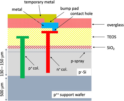
FIGURE 1. Schematic cross-section of 3D small-pitch pixels made at FBK on Si-Si substrates with a single-sided technology (not to scale). The same process is also used for 3D trenched electrodes.
The device processing is made entirely from the front-side. After initial oxidation and implantation of the p-spray surface insulating layer, the p+ (bias) columns are etched with a depth enabling to penetrate into the support wafer, also etching through the bonding oxide in case of SOI wafers [8], so that the bias can be applied from the back side. Next, the n+ (readout) columns are etched stopping at a safety distance of about 25 μm from the support wafer, in order to avoid early breakdown [9]. Both types of columns are doped by thermal diffusion and filled (at least partially) with poly-Si, also leaving small poly-Si extrusions at the column opening (so called “caps”). Several layers of tetra-ethyl-ortho-silicate (TEOS) oxide are deposited to protect the column openings. Contact holes are etched through the upper TEOS layer to make contacts between the metal and the readout column on the poly-Si caps (this is not required for the bias columns that are biased from the back side). An oxide-nitride passivation layer is deposited over the metal, and openings for the bump bonding pads are defined. A temporary metal layer is finally deposited to allow for electrical tests on the pixels, and is removed afterward (more details on the temporary metal are found in “Electrical Measurement Setup” section).
The same technological approach was adopted at FBK for the fabrication of 3D pixels with trenched electrodes on Si-Si substrates, with proper tailoring of the DRIE etching recipes as required by the different geometries of trenched electrodes.
Small-Pitch 3D Pixel Layout
In view of the ATLAS and CMS detector upgrades at the HL-LHC, a new readout chip (ROC) has been developed by the CERN RD53 Collaboration in 65 nm CMOS technology [10]. The first prototype of this ROC, called RD53A, has 400 × 192 pixels, with a total active area of 1.92 cm2. The final versions, that will be different for ATLAS and CMS applications, will be roughly twice as large. Two small-pitch 3D pixel sizes compatible with the RD53A chip, namely 50 × 50 μm2 and 25 × 100 μm2, have been fabricated by all the 3D processing facilities (CNM in Barcelona, Spain; FBK in Trento, Italy; SINTEF in Oslo, Norway) in the R&D phase and qualified for the final production [11]. Both pixel geometries will finally be used to instrument different regions (50 × 50 μm2 in the flat barrel, and 25 × 100 μm2 in the rings) of the innermost pixel layer (Layer 0) of the new ATLAS Tracking System (ITk). For the CMS tracker upgrade, these 3D pixels are still among the options under consideration, but a final decision has not yet been made.
The sketches of different pixels and electrode configurations are shown in Figure 2. The 50 × 50 μm2 3D pixel of Figure 2A was designed only in a version with one readout electrode at the center of a cell (50 × 50−1Ε). In fact, the inter-electrode distance (L) is about 35.4 μm, small enough to effectively counteract charge trapping effects [12], so as to ensure a high radiation tolerance even after the maximum radiation fluences expected in HL-LHC applications. On the contrary, two versions were designed for the 25 × 100 μm2 pixels, featuring either one (25 × 100−1Ε) or two (25 × 100−2Ε) readout electrodes: the former (Figure 2B) has L ∼ 51.5 μm, a not so small value that was initially not considered safe from the radiation resistance point of view (but it was later demonstrated to be good enough); the latter (Figure 2C), owing to a much shorter L ∼ 28 μm, would certainly be more radiation hard, but this would come at the expense of a higher capacitance [11], besides the technological complications that will be detailed in the following.
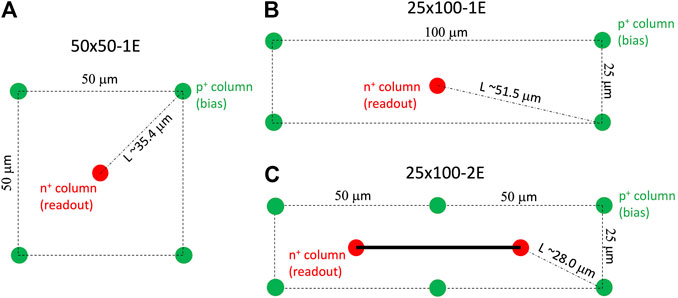
FIGURE 2. Conceptual design of small-pitch 3D pixels for the ATLAS and CMS upgrades at HL-LHC, also indicating the values of the inter-electrode distance L. (A) 50 × 50–1E; (B) 25 × 100–1E; (C) 25 × 100−2E.
Passing from the conceptual designs of Figure 2 to real layouts introduces some constraints. In this respect, the single-sided fabrication approach is less flexible than the double-sided one, since geometrical details (minimum size, minimum distance, minimum overlap, … ) of all layers should be patterned on the front-side only. Depending on the layout rules, which are mainly affected by the lithography equipment, the pixel layout can become critical.
Figure 3 shows the layouts designed for stepper lithography, i.e., with more aggressive layout rules. In case of the 50 × 50−1Ε pixel of Figure 3A, the layout is in fact quite straightforward, also considering that the RD53A has exactly a 50 × 50 μm2 footprint for the bump bonding pads. The layout is not dense, provided the column diameter (5 μm for the readout columns, 6 μm for the bias columns, representative of FBK technology) is small enough. In particular, the bump bonding pad, despite its non-negligible size (12−μm diameter in the passivation opening), can be easily placed on any side of the readout column. Note that the alternative option to place bumps just on top of the readout columns, that would be appealing in several respects, was also successfully tested, but it was not deemed safe enough for the yield of the bump bonding process due to the non-flat surface topography at the column opening. For the 25 × 100−1Ε pixel (Figure 3B), the layout is slightly more complex, because the bump bonding pads should be placed on a 50 × 50 μm2 grid compatible with the footprint of the ROC. This creates an asymmetry between even and odd pixel rows, but the layout density is anyway low enough. On the contrary, the layout of the 25 × 100−2Ε pixel (Figure 3C) is more critical, as evident from its higher density. In particular, the very small distance between the bump pad and the poly-Si cap of bias columns can be a major risk for micro-discharges leading to early breakdown. In the layouts of Figure 3A–B–C the contact between metal and poly-Si on the readout column is made around the column opening with a ring shape. Different layout solutions were also tested for the 25 × 100−2Ε pixels, featuring the so called “ears”. In the “ear” layouts, contacts between metal and poly-Si are offset with respect to the readout columns. Both a vertical offset (Figure 3D) and a horizontal offset (Figure 3E) were implemented.
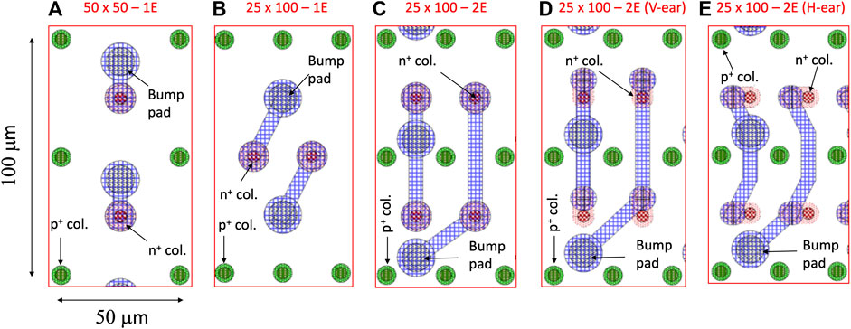
FIGURE 3. Layout of small-pitch 3D pixels for the ATLAS and CMS upgrades at HL-LHC (two adjacent pixels are shown in each slice). (A) 50 × 50–1E; (B) 25 × 100–1E; (C) 25 × 100–2E (D) 25 × 100–2E (V-ear); (E) 25 × 100–2E (H-ear).
Note that for all pixel types a slim-edge (150-μm wide, compliant with the ATLAS ITk specification) termination was designed, based on multiple rows of bias columns that ensure the confinement of the depletion region spreading from the outermost junction columns within a short distance, so that it does not reach the highly damaged cut region [4].
Trenched 3D Pixels Layout
In the past few years, many R&D efforts have been devoted to the development of high-resolution timing detectors as a solution to the problem of high-track density in the detectors of future experiments at particle colliders. While for HL-LHC applications dedicated timing layers, e.g. based on LGAD sensors, will be added to the ATLAS and CMS detectors [13], for experiments at future colliders, e.g., LHCb and FCC, space and time measurements should be combined in a single device [6]. Small-pitch 3D pixels have been shown to offer good timing resolution, but their ultimate performance is limited by the spatial non-uniformity of the electric and weighting fields within a pixel, limiting the timing resolution [14].
To overcome this problem, inspired by the original idea of S. Parker [15], we have started the development of 3D pixel sensors with trenched electrodes, which promise to offer outstanding timing performance while retaining all other advantages of 3D sensors, like radiation hardness [16–18]. Having in mind the LHCb upgrade as an application, in order to be compatible with the readout chips of the MEDIPIX/TIMEPIX family [19] for the first tests, a pixel size of 55 × 55 μm was chosen. Figure 4 shows the conceptual design of a pixel, and its corresponding layout. Although the pixel size is slightly bigger than that of Figure 3a, the layout is much denser. In particular, a critical aspect is represented by the need for the bump pad not to overlap the readout trench, where the surface is not flat, so that the distance between the pad and the poly-Si cap along the bias trench is small. This motivated the use of stepper lithography from the first batch. Note that for in these trenched 3D pixels an active-edge termination is available [2].
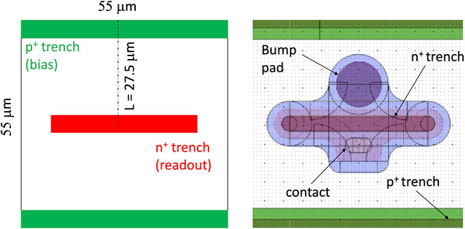
FIGURE 4. Conceptual design (left), and layout (right) of a 3D pixel with trenched electrodes.
3D Sensor Batches at FBK
FBK has so far fabricated three batches of 3D pixel sensors oriented to the HL-LHC upgrades, all made on 6-inch diameter wafers, while two other batches are under way. The first batch, completed in 2015, allowed to assess the fabrication process with promising results: the RD53A chip was not yet available at that time, so the wafer layout included sensors compatible with the ATLAS FEI4 and CMS PSI46dig ROCs, and many test structures [20]. In the second batch, 3D pixel sensors compatible with the RD53A readout chip were fabricated for the first time, with a wafer layout still including several ATLAS FEI4 and CMS PSI46dig compatible sensors [21]. Both the first two batches were made using mask aligner lithography. Since the electrical yield obtained for the 25 × 100−2Ε pixels in batch 2 was not satisfactory, it was decided to use the stepper lithography in batch 3, with a wafer layout entirely dedicated to 3D pixels compatible with the RD53A ROC and test structures.
Figure 5 shows the photographs of two processed wafers from batch 2 and batch 3, whereas Table 1 summarizes the main information on the two batches. Note that both Si-Si and SOI wafers of 130 μm active thickness were used in batch 2, whereas Si-Si of 150 μm active thickness (the substrate of choice for the innermost layers of both the ATLAS and CMS trackers at HL-LHC) were used in batch 3.
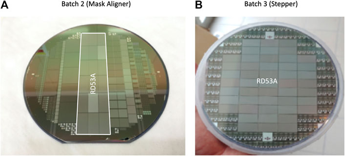
FIGURE 5. Photograph of processed wafers from batch 2 (left) and batch 3 (right): 18 RD53A-compabile sensors are present in a wafer from batch 2, 47 of them in a wafer from batch 3.
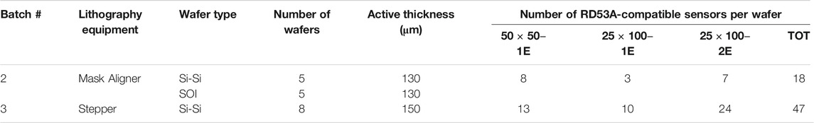
TABLE 1. Overview of FBK 3D small-pitch pixel batches 2 and 3 aimed at ATLAS and CMS upgrades at HL-LHC.
Leveraging the experience on small-pitch 3D pixels and planar active-edge sensors [22, 23], FBK has fabricated one batch of trenched 3D pixels in 2019 within the INFN TIMESPOT project [6]. The batch was made on 6-inch diameter wafers of the same type as those used for the previously mentioned batch 3, with 150-μm active layer thickness. Being this the first prototype batch, many different pixel layouts, differing both in the trench dimensions and the surface layers design, were implemented, along with a number of process splits to test the most critical process steps. In this case, the reticle included full structures to be exposed in a single shot. Since trenched electrodes are causing a larger bow of the wafers as compared to columnar electrodes, it was also decided to keep the number of dies limited, with wide regions of non-etched silicon in between, so as to maximize the mechanical yield [18].
Mask Aligner vs Stepper Lithography
Mask aligners are the simplest and most widely used lithography equipment in radiation detector technologies. The related masks include entire wafer layouts, that are exposed in one single shot on a wafer. The mask is normally kept at a distance (proximity gap, g) of a few tens of micrometers from the wafer, operating in the so-called proximity mode lithography. By doing so, the minimum resolution that can be achieved is
Nevertheless, as can be seen in Figure 3C–E, the layout of the new 25 × 100−2Ε 3D pixels is really dense and involves very small feature sizes, in particular for the minimum distance between the bump bonding pad and the bias columns. Its fabrication requires a resolution and an alignment accuracy that a mask aligner cannot achieve with good process reliability, calling for a better lithography equipment. At FBK a stepper is available having a minimum feature size of 350 nm and an alignment accuracy of 80 nm, good enough for the considered geometries. It was therefore possible to use it in order to assess the feasibility of fabricating 3D pixels with such a critical layout in view of a possible production.
In a stepper mask, called reticle, the device dimensions are magnified (e.g., 5X) and a complex optical focusing system is used to project the reticle image to wafer level [24]. The big distance between reticle and wafer eliminates the defects caused by the small gap or the direct contact between the mask and the wafer in a mask aligner. A related advantage is that the optical inspection of wafers after each lithography, which is normally a very important and time-consuming step for operators with mask aligners, can be greatly simplified with stepper.
In 3D sensor technology, one peculiar aspect is the use of thick photoresist layers to serve also as a masking material (on top of the oxide) during the Deep Reactive Ion Etching process. A thick photoresist degrades the lithography resolution with mask aligner. With stepper, the depth of focus can be controlled, so that the desired resolution can be achieved at the interface between photoresist and oxide, thus allowing for a better definition of the columnar electrode openings.
One drawback with stepper lithography is the limited maximum exposure area, of the order of 4 cm2 for the FBK equipment, which requires stitching in case larger detectors are needed. Although not strictly necessary, stitching was successfully tested in batch 3 at FBK. In fact, two RD53A-compatible sensors would fit into a reticle, but the goal was to fabricate all the different pixel geometries shown in Figure 3. This could have been achieved using several different reticles, each one containing two RD53A-compatible sensor designs. As an alternative, the strategy outlined in Figure 6 was used. Reticle layouts were divided in 16 relatively small blocks of the same size (∼5 × 5 mm2 at wafer level), each corresponding to one specific layer relevant to either an array of 96 × 100 pixels (i.e., one eighth of a RD53A-compatible sensor) or a group of test structures. Each block was selected individually using blades, and printed on wafer according to a pre-defined regular grid footprint. In particular, each layer of a block of 96 × 100 pixels was printed 2 × 4 times to build a full-size RD53A sensor (step and repeat operation); moreover, a frame structure containing a slim-edge termination and the cut lines, included in a different reticle, was printed around. The stepper was programmed to obtain a wafer layout comprising 47 pixel sensors and several blocks of test structures at the periphery (see Figure 5B). By doing so, the number of reticles was largely reduced, at the expense of a complication in the stepper programming, with a very high number of “step and repeat” operations. During batch 3, this sometimes caused an accidental malfunctioning of the stepper, so that the lithography of some layers had to be repeated several times. As a result, the quality of the batch 3 was finally not as good as potentially achievable with a stepper. Nevertheless, the advantages in terms of resolution and alignment accuracy were evident.
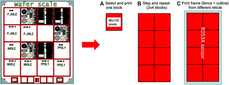
FIGURE 6. Example of reticle layout and exposure strategy used with stepper in batch 3.
As can be seen in Figure 7, a much better control of the 25 × 100– 2E pixel geometry is achieved by stepper lithography with respect to mask aligner. With mask aligner (Figure 7A, also showing temporary metal) the metal is not well aligned with respect to the columnar electrodes; in particular, in the region of the bump pads, the metal is too close and sometimes overlaps the poly-Si cap of the p+ column, so that the entire bias voltage drops on a relatively thin TEOS layer, with major risk of shorts due to the non-ideal step coverage of the TEOS layer at the edge of the poly-Si cap. With stepper (Figure 7B), more aggressive layout rules can be used and be preserved in the real device implementation: in particular, it can be seen that the metal of the bump pad remains at a safety distance from the poly-Si cap of the p+ columns.
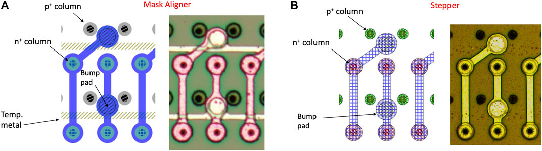
FIGURE 7. Layout details and micrographs of 25 × 100–2E 3D pixels fabricated at FBK with (A) mask aligner (also showing temporary metal strips), and (B) stepper lithography.
The very good pattern definition and alignment accuracy achieved with stepper lithography can also be appreciated from Figure 8, where a Scanning Electron Microscope (SEM) image of the 25 × 100– 2E pixels of Figure 3D (version with vertical ear) is shown. All layout details are preserved: in particular, in the critical region of bump pads all structures are clearly separated.
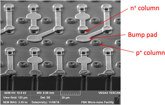
FIGURE 8. SEM micrograph of a 25 × 100–2E 3D pixel (layout version of Figure 3D) fabricated at FBK with stepper lithography.
The superior quality of stepper lithography was also fundamental to successfully fabricate trenched 3D pixels at the first attempt. A SEM micrograph of a group of pixels of the type shown in Figure 4 is reported in Figure 9, showing details of the trenches and of surface topography: in particular, it can be seen that the bump pads (shorted by temporary metal in the picture) are well separated from the poly-Si cap at the opening of the bias trench.
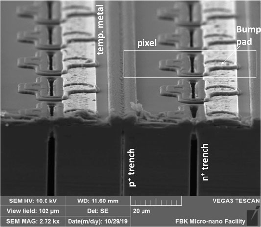
FIGURE 9. SEM micrograph of a group of trenched 3D pixels (see layout in Figure 4) from the first batch fabricated at FBK with stepper lithography.
Electrical Measurement Setup
Pixel sensors were electrically tested at wafer level, at room temperature and in dark conditions, using an automatic probe station with dedicated probe cards. To this purpose, the testing method originally developed for the IBL 3D pixels [4, 7] has been used. A layer of temporary metal is deposited over the passivation and patterned in strips; each strip contacts many pixels through the bump pad openings, shorting them to a common probe pad. Groups of strips are routed to the same probe pad and their current-voltage (I-V) curves are measured in parallel up to 50 V reverse bias. In batch 2, 8 strips of 192 pixels (1,536 pixels, 3.84 mm2 area) were measured in parallel; in batch 3, where the number of RD53A sensors is much bigger, in order to reduce the total measurement time, 20 strips of 192 pixels (3,840 pixels, 9.60 mm2 area) were measured in parallel. It should be noted that the measured currents overestimate the true pixel currents, because of the additional surface current contribution (MOS effect) caused by the temporary metal [7].
The total current of a sensor is then obtained by summing all the strip currents, and sensors are sorted according to the leakage current specifications for the ITk 3D pixels, which are here summarized:
• depletion voltage Vdepl<10 V
• breakdown voltage larger than the operation voltage Vop = Vdepl+20 V
• leakage current at operation voltage I(Vop) < 2.5 μA/cm2.
The depletion voltage is measured from the capacitance-voltage curves of test diodes, and is very low (<3 V). However, as a worst-case condition, the upper limit for depletion voltage was considered, setting Vop at 30 V and comparing the relative current to the specification threshold. Note that if the current respects the specification, also the breakdown voltage condition is practically assessed.
Results
Small-Pitch 3D Pixels
An example of the I-V curves measured with temporary metal on the 20 strips of pixels (3,840 pixels in each strip) in a 25 × 100-2E sensor from wafer 38 of batch 3 is shown in Figure 10A. While this sensor is certainly good, with a total current below 600 nA at 30 V, a non-negligible dispersion of the strip current values can be observed, that is usually measured for 3D technologies [4, 7]. The sum of the 20 strips I-V curves gives then the total sensor I-V curves, as shown in Figure 10B for all the 25 × 100-2E sensors of the considered wafer. It can be seen that about one half of these sensors are functional with low leakage currents and breakdown voltage larger than 50 V (the maximum bias applied in the test), whereas the others either show early breakdown or a smooth raise in the curves finally leading to high leakage values.
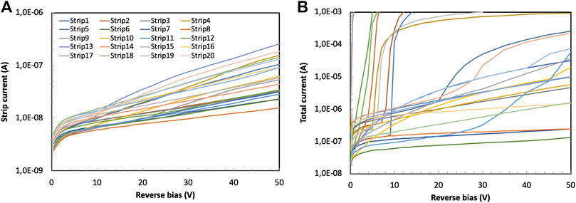
FIGURE 10. I–V curves of 25 × 100–2E 3D pixels from batch 3: (A) currents of all strips (3,840 pixels each) in an individual sensor, and (B) total currents of all sensors in Wafer 38.
In order to have a comprehensive overview of the results, Figure 11 (for batch 2, and distinguishing between the two types of wafers) and Figure 12 (for batch 3) show the distributions of all the strips currents measured at a reverse bias of 30 V. The distributions show several peaks at different leakage current values: the peaks at low leakage currents are mainly to be ascribed to fluctuations from wafer to wafer, and sometimes also within single sensors, whereas the peaks at high leakage currents are due to process defects. As a reference, the specification on the leakage current at the operation voltage I(Vop) < 2.5 μA/cm2, when scaled to the area covered by each strip, corresponds to an upper limit of 96 nA for batch 2 and 240 nA for batch 3. These values are indicated with vertical dashed lines in Figures 11, 12. It can be seen that most of the strips of 50 × 50-1E and 25 × 100-1E pixels have leakage currents well below the specification both in batch 2 and in batch 3, with remarkably low values which, after normalization to the number of pixels, range from a fraction of 1 pA to a few tens of pA per pixel. As a result, the yield of these two geometries for full sensors is expected to be good enough. Conversely, it can be seen that the strips of 25 × 100-2E pixels strips have on average higher leakage currents. This is consistent with the larger electric fields due to the smaller inter-electrode distance, as also reported from CNM [25]. Most important, a significant fraction of the 25 × 100-2E strips have currents above the specification in batch 2 and, to a lesser extent, in batch 3, with obvious impact on the yield for this geometry.
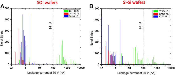
FIGURE 11. Distributions of leakage current at 30 V reverse bias in all 3D strips (1,540 pixels each) from (A) SOI wafers, and (B) Si-Si wafers of batch 2.
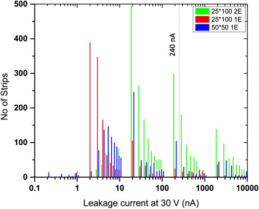
FIGURE 12. Distributions of leakage current at 30 V reverse bias in all 3D strips (3,840 pixels each) from all wafers of batch 3.
Table 2 summarizes the wafer electrical yield of all RD53A-compatible sensors from both batch 2 (for different wafer types and overall) and batch 3. For each sensor geometry, the data correspond to the fraction of sensors meeting the leakage current specification on the total number of sensors present on a wafer, given in Table 1. The average, minimum and maximum values are reported, which reflect relatively wide wafer-to-wafer non-uniformities. On one hand, comparable values of the yield with mask aligner and stepper are found for the two non-critical geometries (50 × 50–1E and 25 × 100–1E), of the order of 60% on average. This result, similar to that obtained from selected wafers in the ATLAS IBL 3D pixel production at FBK [4], is good enough considering the high technological complexity. On the other hand, while remaining lower than for the other two geometries, the yield of 25 × 100–2E pixels roughly doubled in batch 3 as compared to batch 2, reaching almost 40% on average, with minor differences between the different layouts shown in Figures 3C–E. While confirming that the 25 × 100–2E geometry is the most critical, this result is promising and suggests that, in case of an optimized reticle design, also the fabrication of this pixel geometry would be feasible at FBK with an acceptable yield.
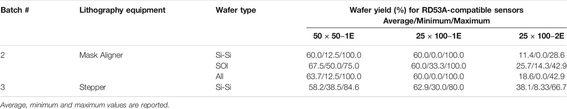
TABLE 2. Summary of the wafer electrical yield for all RD53A-compatible 3D pixel sensors from batches 2 and 3.
Trenched 3D Pixels
The electrical characteristics of the first prototypes of trenched 3D pixels are good. As an example, Figure 13A shows the I-V curves of all pixel sensors (18 × 18 pixel arrays) in a die from Wafer 2,249, whereas Figure 13B shows the distribution of the leakage current at 50 V bias for all the pixel sensors of the considered wafer. Most sensors have leakage current of a few nA, which corresponds to about 10 pA per pixel, a remarkably low value. Note that the depletion voltage is only a few Volts, and the breakdown voltage almost 200 V [17], thus leaving a wide operational margin to operate the pixels with carrier velocity saturation, as requested to enhance the timing performance. The first measurements performed in a beam test on these devices coupled to discrete readout circuits are in fact very promising, showing a timing resolution of about 20 ps [6].
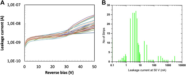
FIGURE 13. (A) I–V curves of all 3D- Trenched-Electrode pixel sensors in a die, and (B) distribution of total leakage current at 50 V. Data refer to arrays of 18 × 18 pixels in Wafer 2,249 from the first batch.
Conclusion
For the development of advanced 3D pixel sensors at FBK, we have started to use stepper lithography in place of mask aligner to profit from the much better definition of critical layout details it can provide.
Despite the problems occurred during the fabrication of the first stepper batch (batch 3), due to the choice to accommodate many design variants and the related complication in the exposure strategy, the overall results are satisfactory. The yield for the critical 25 × 100–2E geometry was largely improved (roughly doubled) with respect to the previous batch using mask aligner (batch 2), reaching almost 40% on average. Conversely, the yields for the other non-critical geometries 50 × 50–1E and 25 × 100–1E remained roughly the same, about 60% on average, that is good enough considering the complex fabrication technology of 3D sensors and the very large density of columnar electrodes involved in small-pitch designs. These results confirm that stepper is a viable solution for the production of advanced small-pitch 3D sensors. Two batches of small-pitch 3D sensors are currently being fabricated at FBK, using a simplified approach to expose in a single shot the sensors and test structures present in a reticle, so as to further improve the yield and the wafer-to-wafer uniformity.
Using the stepper, we have also successfully produced 3D-Trenched Electrode pixel sensors for the first time, showing very low leakage current and high breakdown voltage. A second batch with improved layout is currently being fabricated.
Data Availability Statement
The raw data supporting the conclusions of this article will be made available by the authors, without undue reservation.
Author Contributions
The manuscript was written by G-FDB and MAAS. Conceptual design of the sensors and of the fabrication technology was performed by MB, G-FDB, AL, RM, and MM. Sensor layout was designed by G-FDB, FF, and RM. Process design and sensor manufacturing were carried out by MB, SF, and SR. Electrical measurements at wafer level were performed by FF. Data analysis was performed by MB, G-FDB, FF, and MAAS. All authors reviewed the manuscript.
Funding
This work was supported by the Italian National Institute for Nuclear Physics (INFN), Projects RD_FASE2, FASE2_ATLAS and FASE2_CMS (CSN1), TIMESPOT (CSN5), by the AIDA-2020 project EU-INFRA proposal no. 654168, and by EC under Grant Agreement 777222, ATTRACT-INSTANT project.
Conflict of Interest
The authors declare that the research was conducted in the absence of any commercial or financial relationships that could be construed as a potential conflict of interest.
Acknowledgments
The authors would like to thank D. M. S. Sultan (formerly with the University of Trento and TIFPA INFN, now with the University of Geneva), and Giulio Tiziano Forcolin (formerly with TIFPA INFN) for their contribution to the design of the sensor layout. Fruitful discussions with colleagues from the INFN joint ATLAS-CMS “Phase 2” Pixel R&D project are warmly acknowledged. Special thanks to the technical staff of FBK Micro Nano characterization and fabrication Facility (MNF).
References
1. Parker SI, Kenney CJ, Segal J. 3D–a proposed new architecture for solid-state silicon detectors. Nucl Instrum Methods A (1997) 395:328–43. doi:10.1016/S0168-9002(97)00694-3
2. Da Vià C, Dalla Betta G-F, Parker SI. Radiation sensors with 3D electrodes. Boca Raton, FL: CRC Press (2019), 229.
3. Kenney C, Parker S, Segal J, Storment C. Silicon detectors with 3-D electrode arrays: fabrication and initial test results. IEEE Trans. Nucl. Sci. NS (1999) 46(4):1224–36. doi:10.1109/23.785737
4. Da Via C, Boscardin M, Dalla Betta G-F, Darbo G, Fleta C, Gemme C, et al. 3D silicon sensors: design, large area production and quality assurance for the ATLAS IBL pixel detector upgrade. Nucl Instrum Methods A (2012) 694:321–30. doi:10.1016/j.nima.2012.07.058
5. Dalla Betta G-F, Boscardin M, Darbo G, Mendicino R, Meschini M, Messineo A, et al. Development of a new generation of 3D pixel sensors for HL-LHC. Nucl Instrum Methods A (2016) 824:386–7. doi:10.1016/j.nima.2015.08.032
6. Anderlini L, Aresti M, Bizzeti A, Boscardin M, Cardini A, Dalla Betta G-F, Ferrero M, et al. Intrinsic time resolution of 3D-trench silicon pixels for charged particle detection. J Inst (2020) 15:P09029. doi:10.1088/1748-0221/15/09/P09029
7. Giacomini G, Bagolini A, Boscardin M, Dalla Betta GD, Mattedi F, Povoli M, et al. Development of double-sided full-passing-column 3D sensors at FBK. IEEE Trans Nucl Sci (2013) 60(3):2357–66. doi:10.1109/TNS.2013.2262951
8. Dalla Betta G-F, Boscardin M, Bomben M, Brianzi M, Calderini G, Darbo G, et al. The INFN-FBK “Phase-2” R&D program. Nucl Instrum Methods (2016) 824:388–91. doi:10.1016/j.nima.2015.08.074
9. Sultan DMS, Mendicino R, Boscardin M, Ronchin S, Zorzi N, Dalla Betta G-F. Characterization of the first double-sided 3D radiation sensors fabricated at FBK on 6-inch silicon wafers. J Inst (2015) 10:C12029. doi:10.1088/1748-0221/10/12/C12009
10.The RD53 Collaboration. RD53A integrated circuit specifications (2015). CERN-RD53-PUB-15-001, 18.
11. Terzo S Novel 3D pixel sensors for the upgrade of the ATLAS Inner Tracker. Front Phys Special Issue (2020).
12. Da Via C, Watts S. The geometrical dependence of radiation hardness in planar and 3D silicon detectors. Nucl Instrum Methods A (2009) 603:319–24. doi:10.1016/j.nima.2009.02.030
13. Cartiglia N, Arcidiacono R, Ferrero M, Mandurrino M, Sadrozinski HFW, Sola V, et al. Timing layers, 4 and 5-dimension tracking. Nucl Instrum Methods (2019) 924:350–4. doi:10.1016/j.nima.2018.09.157
14. Kramberger G, Cindro V, Flores D, Hidalgo S, Hiti B, Manna M, et al. Timing performance of small cell 3D silicon detectors. Nucl Instrum Methods (2019) 934:26–32. doi:10.1016/j.nima.2019.04.088
15. Parker SI, Kok A, Kenney C, Jarron P, Hasi J, Despeisse M, et al. Increased speed: 3D silicon sensors; fast current amplifiers. IEEE Trans Nucl Sci (2011) 58(2):404–17. doi:10.1109/TNS.2011.2105889
16. Mendicino R, Forcolin GT, Boscardin M, Ficorella F, Lai A, Loi A, et al. 3D trenched-electrode sensors for charged particle tracking and timing. Nucl Instrum Methods (2019) 927:24–30. doi:10.1016/j.nima.2019.02.015
17. Forcolin GT, Mendicino R, Boscardin M, Lai A, Loi A, Ronchin S, et al. Development of 3D trenched-electrode pixel sensors with improved timing performance. J Inst (2019) 14:C07011. doi:10.1088/1748-0221/14/07/C07011
18. Forcolin GT, Boscardin M, Ficorella F, Lai A, Loi A, Mendicino R, et al. 3D trenched-electrode pixel sensors: design, technology and initial results. Nucl Instrum Methods A 981:2020. doi:10.1016/j.nima.2020.164437
19.The Medipix collaboration, https://medipix.web.cern.ch.
20. Sultan DMS, Dalla Betta G-F, Mendicino R, Boscardin M, Ronchin S, Zorzi N, et al. First production of new thin 3D sensors for HL-LHC at FBK. J Inst (2017) 12(10):C01022. doi:10.1088/1748-0221/12/01/C01022
21. Oide H, Alimonti G, Boscardin M, Dalla Betta G-F, Darbo G, Ficorella F, et al. INFN-FBK developments of 3D sensors for High-Luminosity LHC. Nucl Instrum Methods (2019) 924:73–7. doi:10.1016/j.nima.2018.10.022
22. Povoli M, Bagolini A, Boscardin M, Dalla Betta G-F, Giacomini G, Vianello E, et al. Development of planar detectors with active edge. Nucl Instrum Methods (2011) 658:103–7. doi:10.1016/j.nima.2011.04.050
23. Calderini G, Bomben M, D’Eramo L, Luise I, Marchiori G, Taibah R, et al. Performance of the FBK/INFN/LPNHE thin active edge pixel detectors for the upgrade of the ATLAS Inner Tracker. J Inst (2019) 14:C07001. doi:10.1088/1748-0221/14/07/C07001
Keywords: 3D silicon detectors, stepper, electrical characterisation, fabrication yield, fabrication process
Citation: Boscardin M, Ferrari S, Ficorella F, Lai A, Mendicino R, Meschini M, Ronchin S, Samy MAA and Dalla Betta G-F (2021) Advances in 3D Sensor Technology by Using Stepper Lithography. Front. Phys. 8:625275. doi: 10.3389/fphy.2020.625275
Received: 02 November 2020; Accepted: 10 December 2020;
Published: 18 January 2021.
Edited by:
Paul Sellin, University of Surrey, United KingdomReviewed by:
David Quirion, Institute of Microelectronics of Barcelona (IMB-CNM), SpainMarco Mandurrino, National Institute of Nuclear Physics of Turin, Italy
Copyright © 2021 Boscardin, Ferrari, Ficorella, Lai, Mendicino, Meschini, Ronchin, Samy and Dalla Betta. This is an open-access article distributed under the terms of the Creative Commons Attribution License (CC BY). The use, distribution or reproduction in other forums is permitted, provided the original author(s) and the copyright owner(s) are credited and that the original publication in this journal is cited, in accordance with accepted academic practice. No use, distribution or reproduction is permitted which does not comply with these terms.
*Correspondence: Gian-Franco Dalla Betta, Z2lhbmZyYW5jby5kYWxsYWJldHRhQHVuaXRuLml0