 J. Härkönen1,2*J. Ott2,4A. Gädda2,5
 M. Bezak1,3E. Brücken2E. Tuovinen5S. Bharthuar2P. Luukka2,3
 E. Tuominen2
- 1Ruđer Bošković Institute, Bijenička Cesta, Zagreb, Croatia
- 2Helsinki Institute of Physics, Gustaf Hällströmin Katu, University of Helsinki, Finland
- 3Lappeenranta-Lahti University of Technology, Skinnarilankatu, Lappeenranta, Finland
- 4Aalto University, Department of Electronics and Nanoengineering, Tietotie, Espoo, Finland
- 5Advacam Oy, Tietotie, Espoo, Finland
Radiation hardness is in the focus of the development of particle tracking and photon imaging detector installations. Semiconductor detectors, widely used in particle physics experiments, have turned into capacitive-coupled (AC-coupled) detectors from the originally developed conductively coupled (DC-coupled) detectors. This is due to the superior isolation of radiation-induced leakage current in AC-coupled detectors. However, some modern detector systems, such as the tracking detectors in the CERN LHC CMS or ATLAS experiments, are still DC-coupled. This originates from the difficulty of implementing AC coupling on very small pixel detector areas. In this report, we describe our advances in the detector processing technology. The first topic is the applications of the atomic layer deposition processing technology, which enables the very high densities of capacitance and resistance that are needed when the dimensions of the physical segmentation of pixel detectors need to be scaled down. The second topic is the flip-chip/bump-bonding interconnection technology, which is necessary in order to manufacture pixel detector modules on a large scale with a more than 99% yield of noise-free and faultless pixels and detector channels.
Introduction
The silicon pixel detectors to be used for particle tracking in future high-luminosity colliders will receive very high irradiation doses. In the inner tracker of the Phase-2 CMS experiment, the expected maximum fluence is as high as 2.3 × 10¹⁶ 1MeVneq/cm2. In the inner tracker, two pixel sizes are currently considered by CMS: 25 × 100 μm2 and 50 × 50 μm2 [1].
After such a high dose, the charge carrier mean free path, that is, the drift saturation velocity multiplied by the trapping time, will be of the order of 20–40 µm [2]. However, the pixel segmentation in the devices that are currently used is much larger, typically 100 μm × 100 µm [3]. One approach to maintain adequate charge collection efficiency in planar detectors is to reduce the detector thickness and to increase the detector bias voltage. On the other hand, improving the granularity of the segmented detectors, that is, to downscale the pixel size of the detectors, is important for keeping the detector occupancy low and, thus, the detector position resolution high (occupancy is the number of particles traversing a pixel per event).
The motivation to switch from DC-coupling to AC-coupling arises from the elevated leakage current induced by the accumulated radiation damage caused by incident radiation. The detector leakage current (Ileak) is prevented from being fed to the CMOS read-out ASIC chip (ROC) by the integrated capacitance. The elevated Ileak also has a detrimental effect on the stability of the ROCs that are used in practical radiation detection environments and applications. Some modern and currently operational detector systems are still DC-coupled. The explanation for this is the difficulty of successfully implementing AC-coupling on relatively small pixel areas of the order of 120 × 100 μm2. However, in pixel detectors, it is the patterned top side that is connected to read-out. Thus, the small coupling capacitance on the top of the DC-coupled pixels compared to larger backplane capacitance, or larger capacitance between the neighboring pixels, would result in the collection of charge from wrong contact and, thus, in the failure of detector operation. Namely, the signal is always collected from the area of higher capacitance.
Furthermore, pixel devices could have an n+-implanted surface on the surface of p-type silicon bulk material (i.e., p-type detectors, or n+/p−/p+ devices). Unlike n-type silicon material, p-type silicon material does not undergo space charge sign inversion (SCSI) when exposed to ionizing radiation. Thus, in silicon detectors, the maximum of the electric field collecting the charge carriers beneficially stays on the segmented side of the device even after exposure to high doses of irradiation. Electrons have a higher drift velocity than holes and, thus, are collected into n+ contacts on p-type silicon more efficiently than holes in the traditional detectors that have p+ contacts on n-type silicon [4, 5]. However, among the scientific community, two widely discussed challenges of n+/p−/p+ silicon detectors are, first, the challenges associated with the manufacturing technology and, second, how to compensate the electron accumulation near the interface between the p-bulk silicon and the insulating silicon dioxide (SiO2) layer that characteristically has positive oxide charge. This electron accumulation is unfortunate in p-type silicon detectors because it generates a short-circuiting channel between the n+ pixels [6].
In order to avoid detrimental short-circuits caused by near-surface electron accumulation in p-type detectors, traditional ways include p-spray and p-stops [5]. We used the method of applying a thin-film insulator with a negative oxide charge on the top of the n+ segmentations. We have successfully prepared thin aluminum oxide (Al2O3) layers that naturally have a negative oxide charge by using the method of atomic layer deposition (ALD) [7–9].
Metal-nitride thin films can be deposited, too, using the ALD method. ALD-grown metal-nitride thin films also have the features required by high-quality insulating layers, namely, high precision, high uniformity, and high density of resistance [10]. Silicon pixel detectors are often resistively biased because the electrical current-voltage (IV) quality assurance of the devices is detrimental if performed before the assembly of the detector module by flip-chip (FC) bonding. These bias resistors are commonly manufactured, for example, by using doped poly-silicon or applying punch-through structures [3]. However, when applying these traditional technologies to the small dimensions of pixel segmentation, it is difficult to maintain the bias resistance in the required range of megaohms.
In this report, we present two excellent applications of the ALD technology for solving the challenges in the manufacture of highly segmented pixel detectors with very small dimensions. The first application uses an ALD-grown Al2O3 thin-film field insulator with a natural negative oxide charge in the manufacture of p-type silicon detectors. The second application uses ALD-grown titanium nitride (TiN) thin-film bias resistors in highly segmented pixel detectors.
Magnetic Czochralski Silicon as Substrate Material
Traditionally, silicon radiation detectors have been manufactured using n-type high-resistivity low-impurity float zone (Fz-Si) wafers as the starting material [11, 12]. Consequently, these high-purity Fz-Si wafers also have a very low concentration of oxygen. However, as early as in the 1990s, the CERN RD48 collaboration demonstrated that the diffusion of oxygen into silicon material improved the tolerance of silicon detectors against radiation-induced defects. The RD48 collaboration found that the beneficial concentration of oxygen in silicon detector material is about 1 × 1017 cm−3, which is much higher than that in pure Fz-Si [13, 14].
On the other hand, Czochralski silicon (Cz-Si) has a naturally high and well-controlled concentration of oxygen. Because of the demand for them in micro- and nanoelectronics, sufficiently high-resistivity, that is, 1–10 kΩcm, Cz-Si wafers have been available for the manufacture of radiation detectors since the millennium [15, 16]. Furthermore, in the magnetic Czochralski (MCz) method [17], the silicon ingot is grown in a strong magnetic field so that the concentration and distribution of oxygen and the p-or n-type dopants can be controlled better than in the case of the conventional Cz or Fz crystal growth technologies [18].
Design and Processing of P-Type MCz-Si Pixel Detectors
Our recent pixel detector design consists of two types of sensors suitable for FC bonding with different read-out ASICs: a PSI46dig-geometry AC-coupled pixel sensor with a 200 μm × 100 μm bump pitch and an RD53 A-geometry DC-coupled pixel sensor with a bump 50 μm × 50 μm pitch; see Figure 1. Both the PSI46dig and RD53 A are readout chips (ROCs) currently being used in the CERN CMS experiment [3].
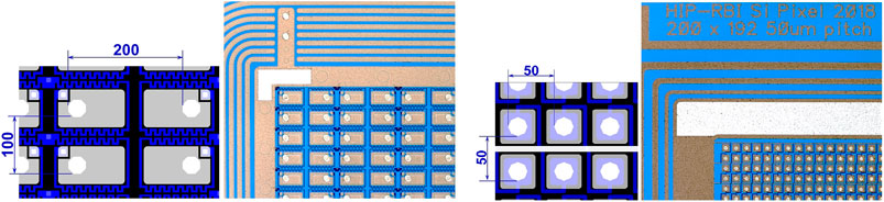
FIGURE 1. Two different pixel detector designs. The pixel design in (A) has a 200 μm × 100 µm pitch compatible with the PSI46 ROC series, which has a 52 × 80 dual-column readout architecture. The design in (B) has a 50 μm × 50 µm pitch compatible with the RD53 collaboration ROC that is under development at CERN [19].
The blue color in Figure 1 indicates sputtered titanium nitride (TiN) thin-film metal bias resistors that allow AC-coupling (Figure 1A) and in the case of DC-signal coupling (Figure 1B) enable current-voltage (IV) measurement before the detectors are connected to readout chips by the FC interconnection method. These detector designs have been published in many conference presentations, and pictures of the entire completed detector wafers in online compilations can be found, for example, in Refs. [20–22]. The detailed detector design, including TCAD simulations and electric field distribution calculations, is published in Ref. [23].
The detector manufacturing process is very similar for both the high-resistivity Cz-Si material and the traditionally used Fz-Si material. The oxygen concentration is the only essential difference between these materials, requiring modified recipes during the back-end process. The detectors described in this report were processed in 2013–2020 at Micronova, the Finnish national research infrastructure for micro- and nanotechnology, jointly run by the VTT Technical Research Centre and Aalto University [24]. Single-side-polished MCz-Si wafers, 150 mm in diameter, 320 µm thick, and with a <100> orientation, provided by Okmetic Oy were used as the starting material [25]. The nominal resistivity of the boron-doped p-type wafers was 6–8 kΩcm. The interstitial oxygen concentration in the particular Si crystal we used was determined by the manufacturer’s production in-line Fourier Transform Infrared Spectroscopy (FTIR) quality assurance (QA) measurement to be 7.5 ppma according to the ASTM F121-83 specifications. 7.5 ppma corresponds to an oxygen concentration of about 4 × 1017 cm−3 [26].
Our detector fabrication process is rather conventional. It contains seven mask levels, including thermal oxidations, ion implantations, ALD depositions, and sputtered metal depositions. A detailed process description, as well as the device design for large-area p-type pixel detectors, is presented in Refs. [27–29]. A tentative process flow is shown in Figure 2. The starting material is >4 kOcm, p-type, 150 mm silicon wafer. The detector process includes two ALD-deposition steps, both n+ and p+ ion implantation steps, two oxidation steps, six lithography steps, seven etching steps, and sputtering and sintering steps. Furthermore, the detector module manufacture includes lithography, sputtering, lift-off, and dicing for making the under-bump metallization for the next step of interconnecting the detector to ROC by FC bonding. Finally, the FC bonded bare-detector module is assembled and wire-bonded to printed circuit board (PCB).
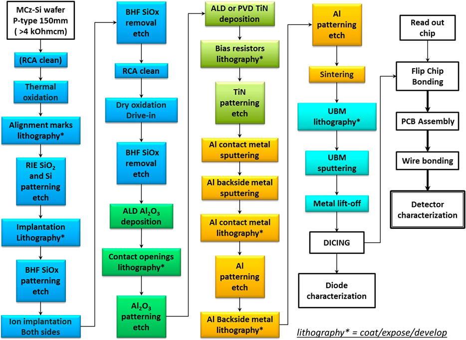
FIGURE 2. Process flow for the manufacture of AC-coupled MCz silicon pixel detectors with ALD-grown thin film.
Between the high-temperature front-end processing steps, that is, in practice thermal oxidations and implanted boron/phosphorus dose activations, the QA was carried out by means of photoconductivity decay (PCD) minority carrier recombination lifetime (τe,h) measurements. The contactless and automated PCD measurement allows the fast mapping of semiconductor wafers reliably monitoring the effective minority carrier recombination lifetime (τeff), which is the combination of the bulk lifetime (τb) and surface recombination limited lifetime (τsr) in different parts of the wafer.
PCD lifetime mappings have been performed on a regular basis during high-temperature detector processing steps, that is, in practice the thermal oxidations of silicon. The lifetime monitor samples are usually Si wafer quadrants as shown in Figure 3A. As an illustrative example, a PCD measurement indicating a localized contamination was selected, as indicated by a red arrow in Figure 3A. The contaminated area appears in the lifetime histogram in Figure 3B as a peak at the value of about 4500 µs.
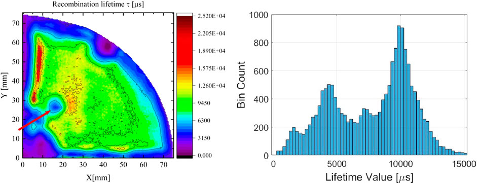
FIGURE 3. (A) Lifetime map of a 150 mm MCz-Si wafer quadrant and (B) a histogram of the numerical lifetime values along the cross-section of the wafer quadrant.
When plotting the numerical histogram, about 2 mm edge exclusion was applied. This was solely due to practical restrictions in the PCD measurement technique. The PCD measurement reveals the minority carrier recombination lifetime in a contactless, non-biased Si wafer, that is, the reflection of the ∼11 GHz microwave signal, depends on the diffusing concentration of electrons/holes. When the quality of the Si is very good and the charge carrier lifetimes are of the order of 10 ms, the carrier diffusion length L of e−/h+ (L = sqrt (diffusion constant × carrier lifetime)) is of the order of the edge exclusion that is applied. Thus, with the PCD method, the regions near the diced edge do not provide meaningful data on the bulk purity of the Si material. However, the detector leakage current, that is, the generation current of e−/h+, has only an insignificant dependence on the silicon bulk properties if the carrier lifetime is more than about 1 ms [30].
P-Type MCz-Si and Thermal Donors
Oxygen thermal donors (TDs) are one of the most studied topics in material physics. It is well known from many studies that TDs are complexes that consist of at least four oxygen atoms and form when silicon wafers are exposed to the typical detector processing temperatures of 400–600 °C. Studies based on computational methods suggest that the formation of TDs and, thus, the formation of shallow donor levels in a silicon band gap are due to the migration of oxygen complex chains [31–34]. In general, when n-type MCz-Si detectors (i.e., p+ segmentation on a phosphorus-donor doped n− bulk) are being processed, the formation of TDs is undesirable since it is equivalent to additional donor doping of the silicon material. Consequently, the additional doping increases the detector operating voltage Vfd. Thus, temperatures above 400 °C should be avoided after the last high-temperature processing step. On the other hand, when p-type detectors (i.e., n+ segmentation on a boron-acceptor doped p− bulk) are being processed, it is possible to tailor the silicon doping by acceptor compensation. Spectroscopic studies of TD formation in detector-relevant high-resistivity silicon materials have been carried out previously and reported in Refs. [35, 36]; see Figure 4.
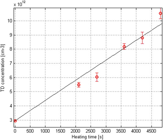
FIGURE 4. Evolution of TD formation in high-resistivity p-type MCz-Si as a function of annealing time at 430 °C.
The samples of the study presented in Figure 4 were diced pad detector diodes, processed on p-type MCz-Si wafers [16]. The nominal resistivity of the boron-doped wafers, as given by the vendor, was 1800 Ωcm, corresponding to an acceptor concentration (Nboron) of about 4.4 × 1012 cm−3. The effective doping concentration (Neff) of the silicon was extracted after each consequent annealing step by capacitance-voltage (CV) probing from the values of the detector full depletion voltage (Vfd). Thus, the thermal donor concentration (NTD) was estimated to be NTD = ❘Nboron - Neff❘ [37].
The samples in this study were processed on Okmetic 150 mm p-type magnetic Czochralski silicon (MCz) wafers. According to the manufacturers production in-line quality assurance (QA) data of LOT 421984–1 16.08.2017, the oxygen concentration in the silicon crystal was 7.5 ppma (ASTM F121-83 specifications, corresponding interstitial oxygen concentration 4.3 × 1017 cm−3) and the resistivity 7 kΩcm. This corresponds to the doping of 1.9 × 10¹² boron atoms/cm3, further corresponding to the full depletion voltage Vfd of about 150 V. In the ready-made pixel detectors, the Vfd was about 60 V, corresponding to the resistivity of 16 kΩcm, further corresponding to the effective doping of 8.3 × 1011 cm−3. The difference of these two values of doping concentrations is the thermal donor concentration, in this case, 1.1 × 10¹² oxygen donors/cm3. This result is very much in accordance with our previous results [37]. However, it is worth noticing that the previous study was done using detectors with different kind of silicon wafer as a starting material and with very unlike oxygen concentration in the silicon crystal. In addition, as shown in Figure 4, previously we studied the silicon samples by annealing them in high temperatures, which is now omitted due to better understanding of thermal donor formation. Thus, in current detector processes, temperatures after oxidation steps are limited to 370 °C.
Passivation by Atomic Layer Deposition Thin Films
An effective method for suppressing the undesirable electron accumulation in the interface between the p-type silicon bulk material and the insulating oxide near the detector surface is to apply a thin-film insulator which naturally has a negative oxide charge. This thin-film insulator must be deposited on the top of the silicon wafer after the high-temperature n+ ion implantations and before the remaining lower-temperature (<400 °C) processing steps.
The values of the negative oxide charge depend strongly on the parameters used during the ALD growth of the aluminum oxide Al2O3. In addition, the interpretation of the capacitance-voltage (CV) data measured from MOS-capacitors for the extraction of the values of the oxide charge requires some assumptions as well as comparison with CV data measured from pad detectors. However, we estimate that values of negative oxide charge in the pixel detectors of this study are as high as 1012 electrons/cm2.
In addition to the negative oxide charge, this thin-film insulator must have a high-quality electrical interface between the oxide and the silicon, and it must be dielectrically strong in order to resist electrical breakdown. The negative oxide charge results in field-effect passivation, that is, repulsing electrons from the oxide-silicon Al2O3-Si interface by means of the Coulomb force. Field-effect passivation of this kind was applied for the first time in the photovoltaic solar cell scientific community [9].
It is worth noticing that ALD-grown aluminum oxide Al2O3 is a field insulator that generates field-effect passivation on the top of the p-type detector. This field insulator is processed on p-MCz Si wafer just after the activation and drive-in diffusion of n+/p+ implantations (see Figure 2). Thus, when manufacturing pixel detectors, the Al2O3 layer gets sintered during the remaining high temperature steps, such as contact metallization, UBM, and FC bonding [27, 37].
As shown in Figure 5, the narrow distribution and the value of the charge carrier lifetime of the as-grown aluminum oxide (Al2O3), which is almost an order of magnitude lower compared to that of sintered Al2O3, indicate that the lifetime in the as-grown Al2O3 was dominated by the surface recombination at the Si-Al2O3 interface. In addition, the lifetime values are clearly higher in sintered Al2O3 than in thermally oxidized silicon dioxide (SiO2).
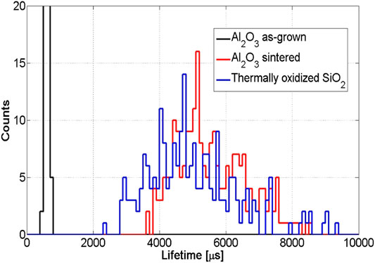
FIGURE 5. Histograms of charge carrier lifetime after ALD deposition of Al2O3 oxide (as-grown, black) and after furnace heat treatment (sintered, blue). As a reference, a thermally dry oxidized SiO2 passivated control sample (RED) providing information about the effective recombination lifetime in silicon bulk material [38].
Pixel Detector Interconnections by Flip-Chip Bonding
The configuration of the pixel detector requires the hybridization of the sensor and the readout chip (ROC) by means of the FC bonding technology (SET FC150 device [39]) see Figure 6 for details. The ROC has tin-lead (SnPb) solder bumps deposited by Advacam Oy [40]. In addition, the sensor pixel pad surface requires a solder-wetting metal known as under-bump metallization (UBM). We prepared a two-layer UBM formed by physical vapor deposition (PVD) MRC [41] magnetron sputtering system [42]. The first layer was a 20 nm thick titanium tungsten (TiW) adhesion layer on which 100 nm thick gold (Au) was deposited. This time, the silicon wafer was diced before the UBM, and the step-pixel patterning of UBM was then performed using a metal lift-off technology. During the FC step, the PSI46dig ROC and sensor were pre-aligned by the optics provided on the FC150 (SET) tool [43]. According to the tool manufacture specification, the post-bonding accuracy is 3 μm. In this detector configuration, thermocompression bonding is used to control the temperature and force while the solder bumps on the pixel contacts and a bump-bond connection are completed in the reflow oven. The eutectic point of SnPb solder is about 184 °C; thus for the hybrid process, it was designed from 184 °C to the reflow temperature, which is plus 20 °C [44] from the eutectic point.
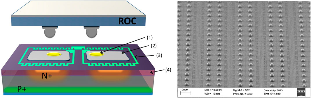
FIGURE 6. (A) Schematic cross-section of a pixel detector module assembly: (1) UBM, (2) Al contact metal, (3) TiN bias resistor, and (4) ALD Al2O3 thin-film passivation layer. (B) SEM picture of SnPb solder bumps on a PSI46dig ROC chip which are used in the silicon tracker of the CERN CMS experiment.
Detector Characterization and Selected Results
For sensor characterization, we have applied commonly adopted methods, namely, CV/IV probe station measurements, transient current technique (TCT) [45–47] measurements, measurements with radioactive sources, and tests for pixel detector modules containing readout chips (ROC) and attached to a data acquisition system (DAQ).
Measurements of the detector full depletion voltage Vfd and leakage current Ileak were performed using probe stations. In addition, the values of Vfd were measured using infrared (IR 1060 nm) laser TCT and extracted from the saturation point of the collected charge (CC). In the TCT measurement, the current generated by the laser pulse is measured from the pixel detector before its interconnection to ROC. For the measurement, the detector is attached to a small auxiliary PCB with conductive glue, and the detector bias rail is wire-bonded to the PCB bonding pad. The signal is collected by attaching a probe needle to the PCB contact pad. (The bonding pad is a bump/FC pad connected to ROC, that is, the signal line. The contact pad is a probe/wire-bonding pad for the DC biasing circuit.) See Figure 7 for the results.
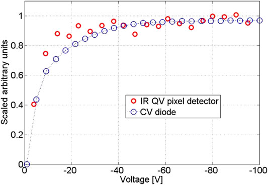
FIGURE 7. IR 1060 nm laser TCT measurement (red) and 1/C2 (blue) showing the voltage saturation point. The detector full depletion voltage Vfd in both cases is about –60 V.
The Vfd was typically between 40 and 60 V in all the pixel sensors that were measured. The homogeneity of the sensors was characterized by TCT scans using both IR and red lasers. The results are presented in Refs. [21, 29, 48]. An illustrative example of such a TCT scan is shown in Figure 8.
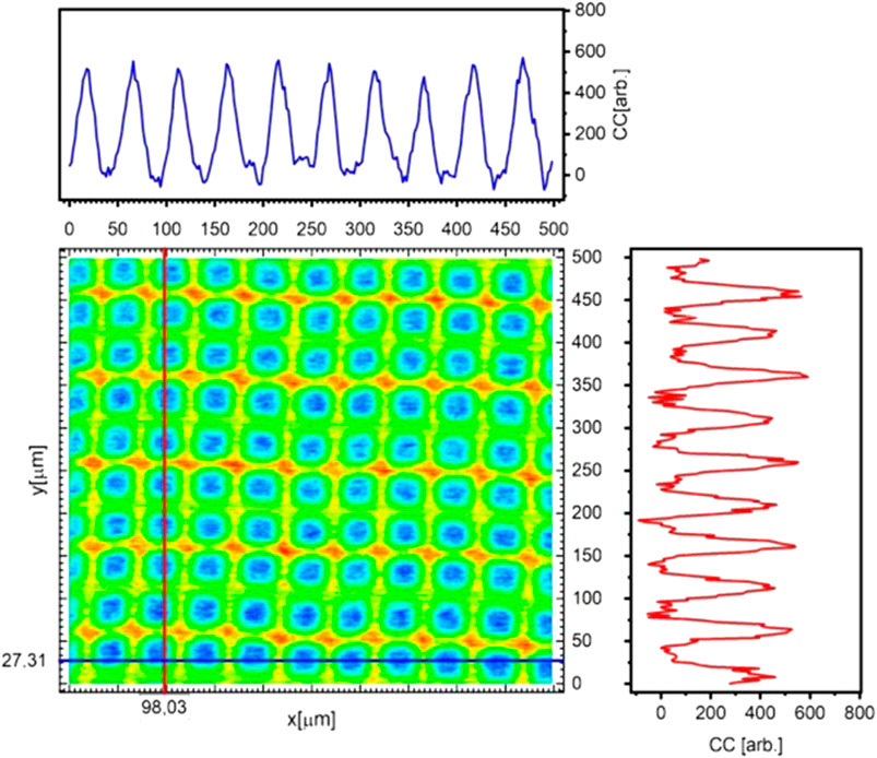
FIGURE 8. IR 1060 nm laser TCT scan of an RD53-type pixel sensor with 50 µm pitch. The excerpt scans measured at points x = 98.03 µm and y = 27.31 µm are presented beside the main xy-scan by blue and red curves, respectively. The scale in the excerpt scans is the same as in the main scan.
The TCT scan area in Figure 8 is 5 × 5 mm2, covering 100 pixels. The highest amplitude is recorded from the bias rails, where, as indicated in Figure 1, the integrated resistors are connected into the n+ -implants. Consequently, the lowest amplitudes originate from the pixels that are covered by aluminum and UBM.
Both electrons and holes contribute to the induced signal current. To investigate the functionality of our AC-coupled pixel detectors, we hybridized the sensor to CMS PSI46dig ROC [49, 50] by FC bonding (FCB). For this purpose, under-bump metallization (UBM) based on a TiW/Au metal stack was prepared on the top of sensors. The hybridized detector assemblies were then tested with radioactive sources, often with Am-241, where the 60 keV main gamma-emission peak results in a charge of about 17,000 electrons if the photon is totally absorbed in the silicon. This is close to the charge generated by a minimum ionizing particle, which is 24,000 electrons in 300 µm thick silicon. This measurement is demonstrated in Figure 9.
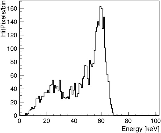
FIGURE 9. Am-241 spectrum of an AC-coupled pixel sensor attached to PSI46dig ROC by flip-chip bonding.
In the pixel readout system developed by the CMS collaboration, the signal triggering takes place by adjusting the threshold level of the readout. The PSI46dig ROC delivers a calibration charge which is expressed and affiliated as Vcal. One Vcal unit corresponds to roughly 50 electrons (e-). In the case of the spectrum presented in Figure 9, the Vcal is 100 arbitrary units, that is, equal to 5000 e−, or to 18 keV energy deposition by the incident Am-241 photons, assuming that the silicon ionization energy is 3.6 eV. Thus, the 26 keV k-line escape peak becomes visible in the Am-241 spectrum to the left of the 60 keV main gamma emission peak.
Summary and Conclusion
For over a decade, we have designed, simulated, modeled, and processed AC-coupled pixel sensors on MCz silicon wafers 150 mm in diameter at the Micronova Nanofabrication Centre. The key principle in our approach is to implement n+/p−/p+ silicon pixel detectors, a field insulator with an oxide charge, and bias resistors made of thin-film metal oxide/nitride materials. This field insulator simultaneously serves as the coupling dielectric for the capacitive signal coupling which isolates the elevated leakage current into the DC-biasing circuit.
The ALD-based thin-film deposition process was optimized and repeatedly applied in our detector fabrication process [29, 30]. Our scanning TCT measurements indicate good homogeneity over large areas and effective electrical isolation between pixels of high density. The IR 1060 nm TCT and CV measurements show systematically full depletion at the voltage of 40–60 V.
Selected pixel sensors were attached by an SnPb-based FC technology to PSI46dig ASIC chips and further connected to an associated front-end readout and DAQ. Fully assembled detectors were used to measure the gamma radiation spectra emitted by the isotope Am-241. According to our results, we are confident about the functionality of AC-coupled n+/p−/p+ pixel detectors with an ALD-grown field insulator and passivation. During the gamma source measurements, the readout and DAQ were set to an electron equivalent triggering threshold of about 5000, allowing the 26 keV AM-241 photopeak to be apparent in the recorded spectrum. Thus, we assume that our pixel sensors would still be operational after the degradation of the charge collection efficiency by 70–80% as a result of the radiation damage induced by heavy hadron irradiation.
Data Availability Statement
The raw data supporting the conclusions of this article will be made available by the authors, without undue reservation.
Author Contributions
All authors listed have made a substantial, direct, and intellectual contribution to the work and approved it for publication.
Conflict of Interest
The authors declare that the research was conducted in the absence of any commercial or financial relationships that could be construed as a potential conflict of interest.
Acknowledgments
This study was partially funded by the Horizon 2020 ERA Chair project, grant agreement 669014 (Particle and Radiation Detectors, Sensors, and Electronics in Croatia, PaRaDeSEC) and by the Academy of Finland project number 314473, “Multi-spectral photon-counting for medical imaging and beam characterization.” JO acknowledges funding from the Viljo, Yrjö, and Kalle Väisälä Foundation of the Finnish Academy of Science and Letters. Detector fabrication was performed in the cleanroom facilities of the Micronova Nanofabrication Centre in Espoo, Finland, within the OtaNano research infrastructure. The authors are grateful to Jaakko Salonen and Vesa-Pekka Lempinen for many fruitful discussions and for their kind assistance.
References
1.CMS Collaboration. The phase-2 upgrade of the CMS tracker (2020). CERN-LHCC-2017-009; CMS-TDR-014. Available from: https://cds.cern.ch/record/2272264?ln=it (Accessed October 30, 2020).
2. Mara B, Michael M. RD50 status report, radiation hard semiconductor devices for very high luminosity colliders (2005). CERN-LHCC-2005-037 and LHCC-RD-009. Available from: https://inspirehep.net/literature/706691 (Accessed October 31, 2005).
3.CMS collaboration. CMS technical design report for the pixel detector upgrade (2012). CMS-TDR-11. Available from: http://cds.cern.ch/record/1481838 (Accessed August 8, 2020).
4. Casse G, Allport P, Martiigarcia S, Lozano M, Turner P. Performances of miniature microstrip detectors made on oxygen enriched p-type substrates after very high proton irradiation. Nucl Instrum Methods Phys Res Sect A Accel Spectrom Detect Assoc Equip (2004) 535(1/2):362–5. doi:10.1016/s0168-9002(04)01688-2
5. Kramberger G, Contarato D. How to achieve highest charge collection efficiency in heavily irradiated position-sensitive silicon detector. Nucl Instrum Methods Phys Res Sect A Accel Spectrom Detect Assoc Equip (2006) 560:98–102. doi:10.1016/j.nima.2005.11.246
6. Pellegrini G, Fleta C, Campabadal F, Miñano M, Lozano M, Rafí JM, et al. Technology of p-type microstrip detectors with radiation hard p-spray, p-stop and moderated p-spray insulations. Nucl Instrum Methods A (2007) 566:360–5.
7. Suntola T. Atomic layer epitaxy. Mater Sci Rep (1989) 4:261–312. doi:10.1016/s0920-2307(89)80006-4
8. Sturm JM, Zinine AI, Wormeester H, Poelsema B, Holleman J, Bankras Radko G, et al. Imaging of oxide charges and contact potential difference fluctuations in atomic layer deposited Al2O3 on Si. J Appl Phys (2005) 97:063709. doi:10.1063/1.1870113
9. Repo P, Talvitie H, Li S, Skarp J, Savin H. Silicon surface passivation by Al2O3: effect of ALD reactants. Energy Procedia (2011) 8:681–7. doi:10.1016/j.egypro.2011.06.201
10. Leskelä M, Ritala M. Atomic layer deposition (ALD): from precursors to thin film structures. Thin Solid Films (2002) 409(1):138–46. doi:10.1016/s0040-6090(02)00117-7
11.G Dhanaraj, K. Byrappa, V. Prasad, and M. Dudley Editors. Springer handbook of crystal growth. Berlin: Springer Science & Business Media (2010).
12. Hartmann F. Evolution of silicon sensor technology in particle physics. Vol. 43. Berlin: Springer (2009).
13. Lindström G, Ahmed M, Albergo S, Allport P, Anderson D, Andricek L, et al. Radiation hard silicon detectors—developments by the RD48 (ROSE) collaboration. Nucl Instrum Methods A (2001) 466:308–26. doi:10.1016/S0168-9002(01)00560-5
14. Härkönen J, Tuominen E, Tuovinen E, Lassila-Perini K, Mehtala P, Nummela S, et al. The effect of oxygenation on the radiation hardness of silicon studied by surface photovoltage method. IEEE Trans Nucl Sci (2002) 49(6):2910–3. doi:10.1109/tns.2002.805345
15. Tuominen J, E , Tuovinen E, Mehtälä P, Lassila-Perini K, Ovchinnikov V, et al. Processing of microstrip detectors on Czochralski grown high resistivity silicon substrates. Nucl Instrum Methods Phys Res Sect A Accel Spectrom Detect Assoc Equip (2003) 514:173–9. doi:10.1016/j.nima.2003.08.102
16. Tuominen J, Tuovinen E, Luukka P, Nordlund HK, Tuominen E. Magnetic Czochralski silicon as detector material. Nucl Instrum Methods Phys Res Sect A Accel Spectrom Detect Assoc Equip (2007) 579:648–52. doi:10.1016/j.nima.2007.05.264
17. Hoshikawa K. Czochralski silicon crystal growth in the vertical magnetic field. Jpn J Appl Phys (1982) 21(9A):L545. doi:10.1143/jjap.21.l545
18. Savolainen V, Heikonen J, Ruokolainen J, Anttila O, Laakso M, Paloheimo J. Simulation of large-scale silicon melt flow in magnetic czochralski growth. J Cryst Growth (2002) 243(2):243–60. doi:10.1016/s0022-0248(02)01441-0
19.RD53 Collaboration. The RD53A integrated circuit. CERN-RD53-PUB-17-001. Available from: https://cds.cern.ch/record/2287593 (Accessed August 8, 2020).
20. Jennifer O, Bharathuar S, Brucken E, Golovleva M, Heikonen J, Gädda A, et al. AC-coupled pixel detectors with aluminium oxide field insulator on p-type MCz silicon. In: 15th Trento Workshop on Advanced Silicon Radiation Detectors in Vienna; Austria (1920).
21. Ott J, Gadda A, Bharthuar S, Brucken E, Golovleva M, Harkonen J, et al. Processing of AC-coupled n-in-p pixel detectors on MCz silicon using atomic layer deposited aluminium oxide. Nucl Instrum Methods A (2020) 958:162547. doi:10.1016/j.nima.2019.162547
22.IRB Infrastructure Developers Ltd. Video Gallery. Available from: http://lnr.irb.hr/PakRaDeSEC/gallery.html (Accessed August 8, 2020).
23. Eremin V, Fadeeva N, Verbitskaya E, Mitina D, Ott J, Härkönen J, et al. Operation of voltage termination structure in silicon n+-p-p+ detectors with Al2O3 field isolator grown by atomic layer deposition method. J Inst Met (2018) 13:P11009. doi:10.1088/1748-0221/13/11/P11009
24.Micronova. Aalto university. Available from: https://www.aalto.fi/en/otanano/micronova (Accessed August 8, 2020).
25.Okmetic. High-performance silicon wafers. Available from: https://www.okmetic.com/ (Accessed August 8, 2020).
26.SEMI. SEMI MF1188. test method for interstitial oxygen content of silicon by infrared absorption with short baseline. Available from: https://store-us.semi.org/products/mf118800-semi-mf1188-test-method-for-interstitial-oxygen-content-of-silicon-by-infrared-absorption-with-short-baseline (Accessed August 13, 2020).
27. Härkönen J, Tuovinen E, Luukka P, Gädda A, Mäenpää T, Tuominen E, et al. Processing of n+/p−/p+ strip detectors with atomic layer deposition (ALD) grown Al2O3 field insulator on magnetic Czochralski silicon (MCz-si) substrates. Nucl Instrum Methods Phys Res Sect A Accel Spectrom Detect Assoc Equip (2016) 828:46–51. doi:10.1016/j.nima.2016.04.069
28. Tuovinen E. Processing of radiation hard particle detectors on Czochralski silicon. [Doctoral Thesis]. Espoo (Finland): Department of Electrical and Communications Engineering, Helsinki University of Technology (2008).
29. Gädda A, Ott J, Bharthuar S, Brucken E, Kalliokoski M. AC-coupled n-in-p pixel detectors on MCz silicon with atomic layer deposition (ALD) grown thin film. Nucl Instrum Methods A (Forthcoming 2020).
30. Härkönen J, Tuominen E, Lassila-Perini K, Palokangas M, Yli-Koski M. Processing and recombination lifetime characterization of silicon microstrip detectors. Nucl Instrum Methods A (2002) 485:159–165. doi:10.1016/s0168-9002(02)00548-x
31. Oehrlein GS. Silicon-oxygen complexes containing three oxygen atoms as the dominant thermal donor species in heat‐treated oxygen‐containing silicon. J Appl Phys (1983) 54:5453–5. doi:10.1063/1.332728
32. Wada K. United model for formation kinetics of oxygen thermal donors in silicon. Phys Rev B (1984) 30:5884. doi:10.1103/physrevb.30.5884
33. Ourmazd A, Schroter W. Oxygen‐related thermal donors in silicon: a new structural and kinetic model. J Appl Phys (1984) 56:1670–81. doi:10.1063/1.334156
34.R. Jones Editor. Early stages of oxygen precipitation in silicon. Dordrecht, The Netherlands: Kluwer Academic (1996).
35. Schröter M, Menichelli D, Scaringella M, Härkönen J, Tuovinen E, Li Z. Thermal donors formation via isothermal annealing in magnetic Czochralski high resistivity silicon. J Appl Phys (2006) 99:093706. doi:10.1063/1.2192307
36. Bruzzi M, Härkönen J, Li Z, Luukka P, Menichelli D, Tuovinen E, et al. Thermal donor generation in Czochralski silicon particle detectors. Nucl Instrum Methods Phys Res Sect A Accel Spectrom Detect Assoc Equip (2006) 568:56–60. doi:10.1016/j.nima.2006.05.201
37. Tuovinen E, Härkönen J, Luukka P, Tuominen E. Intentional thermal donor activation in magnetic Czochralski silicon. Mater Sci Semicond Process (2007) 10(4–5):179–84. doi:10.1016/j.mssp.2007.11.006
38. Härkönen J, Ott J, Mäkelä M, Arsenovich T, Gädda A, Peltola T, et al. Atomic layer deposition (ALD) grown thin films for ultra-fine pitch pixel detectors. Nucl Instrum Methods Phys Res Sect A Accel Spectrom Detect Assoc Equip (2016) 831:2–6. doi:10.1016/j.nima.2016.03.037
39.Smart Equipment Technology. FC150 Specifications. Available from: http://www.set-sas.fr/en/pp422408-421389-FC150.html (Accessed December 14, 2020).
40.ADVACAM. Radiation Imaging Solutions. Available from: https://advacam.com/ (Accessed August 8, 2020).
41.MRC. MRC 903—System Control Techologies. Available from: https://sctec.com/standard-systems/replicated-systems/mrc/mrc-903/ (Accessed December 14, 2020).
43.Smart Equipment Technology. High accuracy bonder. Available from: http://www.set-sas.fr/en/ (Accessed September 12, 2020).
44.IPC-7530. IPC-7530: the definitive guide for temperature profiling for mass soldering (reflow and wave) processes. In: Soldering and surface mount technology. Vol. 13(3). Bingley: Emerald Group Publishing Limited.
45. Eremin V, Strokan N, Verbitskaya E, Li Z. Development of transient current and charge techniques for the measurement of effective net concentration of ionized charges (Neff) in the space charge region of p-n junction detectors. Nucl Instrum Methods Phys Res Sect A Accel Spectrom Detect Assoc Equip (1996) 372:388–98. doi:10.1016/0168-9002(95)01295-8
46. Strokan V, Li Z. Determination of the fermi level position for neutron irradiated high resistivity silicon detectors and materials using the transient charge Technique (TChT). IEEE TNS (1994) 41(6):1907–12. doi:10.1109/23.340522
47.Particulars. Advanced measurement systems.Available from: http://www.particulars.si/index.php (Accessed August 8, 2020).
48. Bezak M. TCT characterization and scanning of fine pitch of n+-in-p pixel detectors. In: 15th Trento Workshop on Advanced Silicon Radiation Detectors in Vienna; Austria (2020).
49. Spannagel S, Perrey HC, Meier B. The pxarCore library—technical documentation, reference manual, and sample applications. Tech Rep (2016). CMS NOTE-2016/001. Available at: http://cds.cern.ch/record/2137512/files/ (Accessed March 8, 2016).
Keywords: pixel detector, atomic layer deposition, magnetic Czochralski silicon, capacitive coupling, carrier lifetime
Citation: Härkönen J, Ott J, Gädda A, Bezak M, Brücken E, Tuovinen E, Bharthuar S, Luukka P and Tuominen E (2021) Processing and Interconnections of Finely Segmented Semiconductor Pixel Detectors for Applications in Particle Physics and Photon Detection. Front. Phys. 9:601730. doi: 10.3389/fphy.2021.601730
Received: 01 September 2020; Accepted: 14 January 2021;
Published: 19 February 2021.
Edited by:
Angela Kok, SINTEF Digital, NorwayReviewed by:
Francesco Moscatelli, National Research Council (CNR), ItalyAdriano Lai, National Institute of Nuclear Physics of Cagliari, Italy
Copyright © 2021 Härkönen, Ott, Gädda, Bezak, Brücken, Tuovinen, Bharthuar, Luukka and Tuominen. This is an open-access article distributed under the terms of the Creative Commons Attribution License (CC BY). The use, distribution or reproduction in other forums is permitted, provided the original author(s) and the copyright owner(s) are credited and that the original publication in this journal is cited, in accordance with accepted academic practice. No use, distribution or reproduction is permitted which does not comply with these terms.
*Correspondence: J. Härkönen, amFha2tvLmhhcmtvbmVuQGlyYi5ocg==