 Stefano Terzo1*
 Maurizio Boscardin2
 Juan Carlotto1
 Gian-Franco Dalla Betta3,4
 Giovanni Darbo5Ole Dorholt6Francesco Ficorella2Giuseppe Gariano5
 Claudia Gemme5Giulia Giannini1
 Sebastian Grinstein1,7
 Andreas Heggelund6
 Simon Huiberts8
 Angela Kok9Ozhan Koybasi9
 Alessandro Lapertosa5,10Magne Elk Lauritzen8Maria Manna11Roberto Mendicino2,3,4Hideyuki Oide5Giulio Pellegrini11Marco Povoli9
 David Quirion11Ole Myren Rohne6Sabina Ronchin2Heidi Sandaker6Md. Arif Abdulla Samy3,4Bjarne Stugu8Leonardo Vannoli5,10
- 1Institute for High Energy Physiscs (IFAE), Barcelona Institute of Science and Technology (BIST), Barcelona, Spain
- 2Bruno Kessler Foundation (FBK), Trento, Italy
- 3Trento Institute for Fundamental Physics and Applications (TIFPA), University of Trento, Trento, Italy
- 4Department of Industrial Engineering, University of Trento, Trento, Italy
- 5National Institute of Nuclear Physics (INFN) of Genova, Genoa, Italy
- 6Department of Physics, University of Oslo, Oslo, Norway
- 7Catalan Institution for Research and Advanced Studies (ICREA), Barcelona, Spain
- 8Department of Physics and Technology, University of Bergen, Bergen, Norway
- 9SINTEF DIGITAL, Oslo, Norway
- 10Department of Physics, University of Genoa, Genoa, Italy
- 11Centre Nacional de Microelectrónica (CNM), Consejo Superior de Investigaciones Científicas (CSIC), Barcelona, Spain
The ATLAS experiment will undergo a full replacement of its inner detector to face the challenges posed by the High Luminosity upgrade of the Large Hadron Collider (HL-LHC). The new Inner Tracker (ITk) will have to deal with extreme particle fluences. Due to its superior radiation hardness the 3D silicon sensor technology has been chosen to instrument the innermost pixel layer of ITk, which is the most exposed to radiation damage. Three foundries (CNM, FBK, and SINTEF), have developed and fabricated novel 3D pixel sensors to meet the specifications of the new ITk pixel detector. These are produced in a single-side technology on either Silicon On Insulator (SOI) or Silicon on Silicon (Si-on-Si) bonded wafers by etching both n- and p-type columns from the same side. With respect to previous generations of 3D sensors they feature thinner active substrates and smaller pixel cells of 50 × 50 and 25 × 100 µm2. This paper reviews the main design and technological issues of these novel 3D sensors, and presents their characterization before and after exposure to large radiation doses close to the one expected for the innermost layer of ITk. The performance of pixel modules, where the sensors are interconnected to the recently developed RD53A chip prototype for HL-LHC, has been investigated in the laboratory and at beam tests. The results of these measurements demonstrate the excellent radiation hardness of this new generation of 3D pixel sensors that enabled the project to proceed with the pre-production for the ITk tracker.
1 Introduction
The Large Hadron Collider (LHC), located at CERN, is the world’s largest and most powerful particle accelerator. ATLAS is one of two general-purpose detectors at the LHC. In order to advance our understanding of elementary particles and their interactions, the LHC accelerator will be improved to be able to reach about seven times its current nominal instantaneous luminosity. The High Luminosity LHC (HL-LHC) is currently foreseen to start operations in 2027. To cope with the higher particle rate, hit occupancy and radiation damage associated with the HL-LHC period, and maintain the overall detector performance, several ATLAS sub-systems will have to be upgraded. In particular, the current ATLAS tracking system will be replaced by a full silicon detector, called ITk, composed of an inner pixel detector surrounded by a micro-strip system. Located in the immediate proximity of the proton-proton beam collision region, the silicon pixel system is critical for the precise determination of particle tracks and vertices, allowing the identification of b-jets (b-tagging). The HL-LHC presents an unprecedented challenge to the silicon pixel sensor technologies: the detector has to provide excellent position resolution while sustaining radiation levels exceeding
A new generation of 3D sensors has been designed to fulfill the requirements in terms of occupancy and radiation hardness for the innermost layers of the ITk pixel detector at the HL-LHC. 3D sensors are an established technology that has been already employed in experiments at the LHC such as in the ATLAS Insertable B-Layer (IBL) [1] and for the tracker of the AFP experiment [2]. With respect to these designs the new ITk 3D sensors feature a reduced pixel cell size of 25 × 100 and 50 × 50 µm2 with one collecting electrode. In the following these pixel cell geometries will be abbreviated as 25 × 100-1E and 50 × 50−1E. A 25 × 100 µm2 pixel cell design with two electrodes (25 × 100−2E) was also investigated, but eventually dropped because of technical difficulties in achieving a satisfactory production yield. All these sensor designs are compatible with the future ATLAS readout chip, the ITkPix. Moreover, in order to lower the occupancy, the thickness of the active substrate of these new sensors is reduced to 150 µm in comparison to the previous generation of 230 µm thick 3D sensors. To achieve such thickness the use of a single-side technology was necessary.
This paper will describe the design and the technological challanges of the recent 3D sensor productions for ITk as well as the results of the characterization performed on assembled module prototypes to validate the performance of these novel 3D sensor designs.
2 The ITk Pixel Detector
The ATLAS detector [3] at the CERN LHC accelerator complex is the largest volume detector ever constructed for a particle collider. ATLAS has the dimensions of a cylinder, 46 m long, 25 m in diameter, and sits in a cavern 100 m below ground. The ATLAS detector weighs 7,000 tonnes and consists of six different detecting subsystems wrapped concentrically in layers around the collision point to record the trajectory, momentum, and energy of outgoing particles, allowing them to be individually identified and measured. A huge magnet system bends the paths of the charged particles so that their momenta can be measured. As mentioned above, the ATLAS subsystems have to be upgraded in view of the challenges of the HL-LHC. The current tracking system will be completely replaced by the new ITk tracking detector.
2.1 Layout
The ITk tracker is composed of an inner Pixel Detector, followed by the Strip Detector (Figure 1). The Strip Detector covers a pseudo-rapidity of
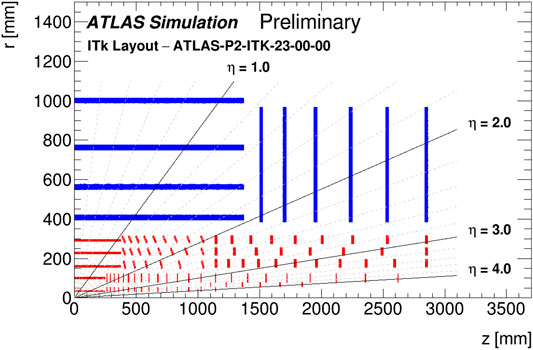
FIGURE 1. Sketch of a quarter of the ITk detector. The Strip Detector is shown in blue, while the Pixel Detector is shown in red.
2.2 The HL-LHC Challenges
The HL-LHC presents two key challenges to the ATLAS experiment: while the detector has to cope with unprecedented radiation levels, it also has to be able to disentangle the huge amount of simultaneous events that will be generated in the proton-proton beam collisions. This is especially critical for the innermost silicon pixel layer, since it is the one that suffers the higher radiation levels and has to operate in the most dense particle environment. Thus, the inner layers of the ITk tracker demand the most radiation hard technology, but at the same time small pixels and thin active regions to mitigate the effect of the high particle multiplicity. These two requirements could be seen as competing, since, in standard silicon devices, thinner sensors usually collect less charge and thus are more sensitive to charge trapping effects introduced by radiation damage.
The HL-LHC period is expected to deliver a total integrated luminosity of 4,000 fb−1, however, the ITkPix front-end is not expected to survive the large radiation doses associated with this scenario. The current strategy foresees replacement of the two inner layers. From the sensor point of view, the expected maximum particle fluence in the innermost layer (
2.3 The ITk Pixel Front-End Chip
The front-end chip integrates the charge generated in the sensor by crossing particles, amplifies and digitizes the signal, and sends the hit information downstream to the DAQ system. The ITk pixel readout chip, called ITkPix, will present a matrix of 400 × 384 pixels of 50 × 50 µm2, which determines the active area of the chip. The ITkPix is based on the prototype chip developed by the RD53 Collaboration, the RD53A [4]. The RD53A readout chip presents a matrix of 400 × 192 pixels of 50 × 50 µm2 with a total size of 20.0 × 11.8 mm2. The ASIC, also fabricated in the 65 nm CMOS technology, includes three different analog front-end designs to allow performance comparisons. These are the synchronous, linear and differential front-ends. The latter has been selected by the ATLAS Collaboration for the development of the final ITkPix chip for ITk.
Measurements of bare RD53A chips and modules (the chip interconnected to a pixel sensor) have shown that the ASIC achieves the desired functionality and can operate at a low threshold, which is a fundamental parameter to ensure high hit reconstruction efficiency after irradiation as it will be discussed below.
2.4 Sensor Requirements
Sensors shall be interconnected to the ATLAS ITk pixel front-end chips which impose a maximum capacitance per pixel of 100 fF. In the innermost layer the 3D modules are attached in groups of three to a single flex readout board (triplet) sharing the same bias voltage line connecting them in series. To ensure the proper operation of the sensors in this configuration, before irradiation the depletion voltage (
As mentioned above, the innermost layer imposes strict requirements in terms of performance after irradiation. With the replacement strategy, the fluence for the innermost pixel layer will exceed
3 3D Silicon Sensors
3.1 Single-Side Approach
Double-sided technologies, which proved to offer several advantages in terms of process complexity and throughput for the IBL production [5], are not favored for the fabrication of thin 3D pixels, due to mechanical integrity considerations. As a result, a single-side approach with a support wafer has finally been adopted by all the processing foundries. As compared to the technology developed in Stanford in the late 1990’s, the process has been modified to be compatible with Si-on-Si wafers, which consist of a high-resistivity float zone active layer of the desired thickness directly bonded to a low-resistivity Czochralski handle wafer of adequate thickness, that might be different depending on the wafer diameter. All columnar electrodes are etched from the front-side and are (at least partially) filled with poly-Si: the junction (readout) columns stop at a safety distance of
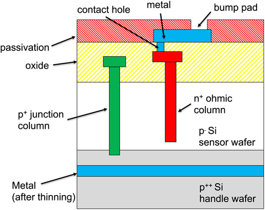
FIGURE 2. Schematic cross section of 3D pixels made from Si-on-Si bonded wafers. All the columns are etched from the top side. The handle wafer is thinned down to the desired thickness before depositing the metal on the backside.
3.2 Small Pixel Cells
On one hand, small pixel cells involve small inter-electrode distances, which inherently improves the radiation hardness, since they can be made comparable to the maximum drift length of charge carriers [6]. On the other hand, a high density of columnar electrodes could also result in a loss of geometrical efficiency, since the electrodes themselves are not efficient, as well as in an increase of the sensor capacitance (and noise). However, both these problems are attenuated by the use of thin active layers: 1) the electrode capacitance scales with its depth to a large extent, so thinner substrates naturally lead to smaller capacitance; 2) assuming the aspect ratio (depth to diameter) attainable with Deep Reactive Ion Etching (DRIE) to be constant (typical values range from
The layout of small 3D pixel cells is quite straightforward, provided the device geometries are all down-scaled. As an example, Figure 3 shows the pixel layouts, specific to the FBK technology, for the three considered geometries.
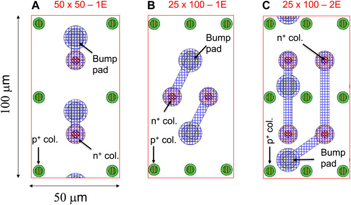
FIGURE 3. 3D pixel layouts, showing pairs of adjacent pixels (FBK version).
It can be seen that the main constraint is due to the fixed size (
4 Foundries and Productions
Productions of 3D sensors compatible with RD53A chips have been carried out at CNM, FBK, and SINTEF. These productions all employ a single-side approach either with Silicon-On-Insulator wafers (SOI) or Silicon-On-Silicon wafers (Si-on-Si). Even if in some productions the thickness is still less with respect to the design specifications of the final sensor (130 µm in FBK, and 50 µm or 100 µm in SINTEF sensors), most of the results can be considered as worst-case scenarios due to the reduced number of initial charge carriers generated by Minimum Ionising Particles (MIPs). Indeed, a thicker active substrate is expected to perform better in terms of charge collection and hit efficiency before and after irradiation. Additional significant differences between the foundry prototype designs are: the edge termination, obtained with an edge doping (active edge) at SINTEF and instead with p-type column fences in CNM and FBK (slim edge design [5]); and the inter-pixel surface insulation where FBK and SINTEF use p-spray, while CNM uses p-stop rings around the n-type columns.
4.1 CNM: Run 9761 and Run 11119
CNM 3D sensor technology was developed first on double-sided detectors in 2006 [7, 8] for the IBL [1] detector of the ATLAS experiment. The double-sided 3D detectors were fabricated on four-inch wafers with columns of one doping type etched from the front side of the device, and the other type etched from the backside. In this technology all columns are only partially passing through the active bulk stopping at about 30 µm from the sensor surfaces.
To reduce the thickness of the active volume, CNM developed ultra-thin 3D single-sided detectors for Neutral Particle Analysers (NPA) and thermal neutron detection in 2009 [9]. This technology was the basis for the development of the upgrade of the ATLAS Inner Tracker. Initially, the detectors were fabricated on SOI wafers with a p-type backside implant and a total thickness of 400 µm [10]. The active thickness is composed of a 150 µm (or 100 µm) thick p-type wafer with a nominal resistivity in the range 10–50 k
Run 9761 was the first run including pixel designs compatible with the RD53A chip. The majority of the wafer layout of this run is devoted to RD53A sensors, named as the corresponding readout chip, with 50 × 50−1E pixel geometry. Each of these sensors holds a matrix of 400 × 192 pixels with a total size of 20 × 11.8 mm2 including 150 µm per side of p-type column fences filling the space between the last pixel cell and the dicing edge. Each wafer also includes two RD53A sensors with 25 × 100−1E pixel and two with 25 × 100−2E pixel geometry. These are both matrices of 200 × 384 pixels with the same total size of the 50 × 50−1E design including the p-type column fences at the edge.
Typical electrical characteristics of the different sensor geometries in this run, as measured on dedicated 3D diodes, are shown in Figure 4. The C-V curves show a depletion voltage lower than 5 V, when the capacitance saturates, with small differences depending on the specific pixel geometry in agreement with the simulation reported in [11]. The I-V characteristics show that a rectifying p-n junction has been formed between the electrodes. The breakdown voltage can be larger than 100 V for the 50 × 50−1E and the 25 × 100−1E geometries and it is in general lower for the 25 × 100−2E, but it should be considered that the full depletion voltage foreseen for these devices is very low. Therefore, the detectors can be operated in over-depleted mode without any constraint. A larger reverse leakage current density and a lower breakdown voltage are measured for sensors with 25 × 100−2E pixel geometry which have a smaller inter-electrode distance. This may be due to the increase of the electric field among the electrodes for the same bias applied.
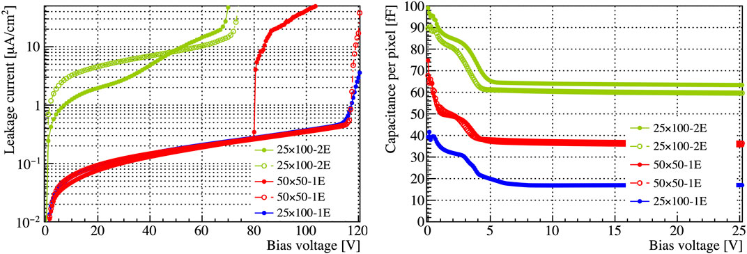
FIGURE 4. CNM 3D diode measurements performed on wafer at the end of the process on the final metal. I-V (left) and C-V (right) curves are shown. A systematic uncertainty, not shown in the figures, of less than 10% has been estimated for both current and capacitance measurements, due to temperature variations and the LCR circuit, respectively. The systematic uncertainties due to the test instrument for the considered voltage and current range are smaller than 1%.
In order to simplify the fabrication process and avoid the etching of the handle wafer, Si-on-Si bonded wafers were chosen for the production of 3D detectors of the ATLAS Inner Tracker. The first run with these Si-on-Si wafers (11119) was produced using a total thickness of 350 µm where 150 µm is the active layer and 200 µm the handle wafer. Around 70% of the RD53A 50 × 50−1E sensors and more than 50% of the RD53A 25 × 100−1E sensors produced in this run have a breakdown voltage higher than 25 V, whereas the 25 × 100−2E configuration suffers from a very low yield and could be very problematic for a large production.
4.2 FBK: 2nd and 3rd Batches
FBK started to develop 3D sensor technologies on four-inch wafers in 2004, in collaboration with INFN. For a few years the focus was on double-side fabrication processes, and led to the development of two device versions: one with columnar electrodes partially passing through the substrate [12], and another one with full-through electrodes [13]. The latter was the technology of choice for the ATLAS IBL 3D pixel production: for this application FBK introduced the slim-edge design based on p-type column fences and the temporary metal for the on-wafer electrical characterization of pixel sensors before bump bonding [5].
After the completion of the IBL production, FBK upgraded its clean room to allow production on six-inch wafers, that require a minimum thickness of 300 µm to ensure a sufficient mechanical robustness. Therefore, given the requirement of a thin active thickness for the HL-LHC upgrades, FBK deemed more appropriate to develop a new generation of small-pitch, thin 3D sensors with a single-side process, pioneering the use of Si-on-Si substrates [14].
After producing a first R&D batch in 2015 [15], mainly aimed at the technology development, FBK produced two batches oriented to the ITk project. All these batches were made on six-inch diameter wafers. The second batch was made in 2017 using mask aligner lithography [16]. The wafer layout included 18 pixel sensors of different geometries compatible with the RD53A chip: 25 × 100−1E (three samples), 25 × 100−2E (seven samples), and 50 × 50−1E (eight samples). Many other sensors compatible with the ATLAS FE-I4 and CMS PSI46dig readout chips were also present, as well as test structures (mainly 3D diodes and strips). This second batch consisted of ten wafers (five SOI and five Si-on-Si) with 130 µm active thickness. The third batch was made in 2019 using stepper lithography. The wafer layout was arranged to host 47 RD53A-compatible pixel sensors of different geometries: 25 × 100−1E (ten samples), 25 × 100−2E (24 samples), and 50 × 50−1E (13 samples), as well as test structures. The third batch consisted of eight wafers (all Si-on-Si) with 150 µm active thickness.
Although the very large variety of different layout options and process splits implemented in both the second and third batches prevent accurate calculation of the fabrication yield, some preliminary conclusions can be drawn from the electrical characterization of the RD53A-compatible pixel sensors. In the second batch, about 60% of the 50 × 50−1E and 25 × 100−1E meet the specifications described in Section 2.4, although with large non-uniformities from wafer to wafer. On the contrary, these percentages fall to less than 20% for the more critical 25 × 100−2E sensors. This motivated the use of stepper lithography in the third batch, in order to improve the pattern definition and layer alignment which are essential for such a dense layout.
Despite the choice to accommodate many design variants, which caused the stepper to be operated in a non-optimal way, in the third batch the percentage of 50 × 50−1E and 25 × 100−1E sensors meeting the specifications was still about 60%, as in the second batch. On the contrary, for the 25 × 100−2E sensors, the percentage doubled with respect to the second batch, reaching almost 40%. While this result is still worse than for the other geometries, it confirms that by using stepper lithography in an optimized way, FBK would be able to produce also this critical sensor layout.
4.2.1 Electrical Characteristics
Besides measurement of the I-V characteristics of pixel sensors using the temporary metal, the quality of 3D sensors from different batches is monitored at FBK by measuring test diodes. These devices reproduce the electrode configurations and layout details (including the edge region) of their parent pixel sensors, but, due to their small size (
As an example, the I-V and C-V curves of diodes from the third batch are shown in Figure 5. The leakage currents of Figure 5 Left are very small: after normalization to the number of columns present in each diode, their values at 25 V reverse bias (much larger than the depletion voltage) are
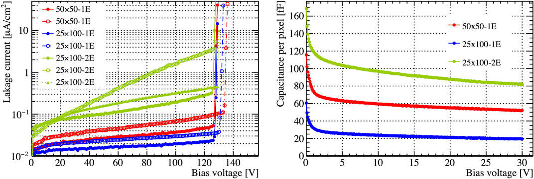
FIGURE 5. FBK 3D diode measurements performed on wafer at the end of the process on the final metal. I-V (Left) and C-V (Right) curves are shown. A systematic uncertainty, not shown in the figures, of less than 10% has been estimated for both current and capacitance measurements, due to temperature variations and the LCR circuit, respectively. The systematic uncertainties due to the test instrument for the considered voltage and current range are smaller than 1%.
In the C-V curves of Figure 5 Right, the knee at low voltage (
4.3 SINTEF: Run 4 and Run 5
The SINTEF 3D sensor technology was developed as single-sided from the beginning, initially on four-inch SOI wafers and, more recently, on six-inch Si-on-Si wafers. The technology features columnar electrodes completely filled with polysilicon and an active edge, a doped trench around the sensor that allows for termination of the active volume with minimal inactive material along the edge of the detectors.
SINTEF has currently produced a total of five batches of 3D silicon sensors. The early production runs delivered good electrical yield but they showed some weakness from the point of view of the mechanical yield. This issue was solved in more recent iterations, which also delivered improved electrical yield.
The first 3D sensor batch fabricated at SINTEF including small-pitch 3D pixel detectors was completed in early 2018. This sensor production, known as “run 4”, was carried out on Si-on-Si wafers with active thicknesses of 50 and 100 µm. The layout of run 4 was mostly focused on FE-I4 pixel detectors but also included two detectors compatible with the RD53A chip, in 50 × 50−1E configuration. In addition, other flavors of pixel detectors were available, compatible with the MediPix, FE-I3 and CMS PSI46 readout chips.
The latest 3D sensor batch fabricated at SINTEF, “run 5”, was completed in January 2020. Produced on Si-on-Si wafers with active thickness of 150 µm, run 5 featured two different layouts (12 wafers per layout) including both RD53A and ITkPix compatible sensors. The first layout was fully tailored to the 50 × 50−1E pixel configuration, while the second layout was split into two parts, the top part of the wafers for 25 × 100−1E sensors and the bottom part of the wafer for 25 × 100−2E sensors. Each layout had 3D diodes and strip detectors with the same electrode pitch as the main pixel detectors in addition to standard planar test structures for process monitoring. Both layouts still featured the active edge. The fabrication procedure was similar to the one used in run 4, with some minor modifications that also included extra quality assurance procedures at critical steps in the process. Particular care was taken in monitoring oxide thicknesses and evolution of the wafer curvature during the process. After deposition of the temporary metal layer, the electrical characterization of the sensors was carried out on wafer using an automatic probe station. After completion of the measurements, the temporary metal layer was removed and the final metal layer deposited. The final passivation was then deposited and patterned and a final inspection of the wafers was completed.
The overall electrical yield of run 4 was excellent, with over 70% of sensors on average across the different pixel configurations showing properties compatible with the requirements described in Section 2.4. Unfortunately, due to the tight layout of the active edge, the pads on the temporary metal for the small-pitch RD53A pixel configuration were too small to be contacted manually and a full on-wafer estimate of the yield was not possible for these devices.
A reliable estimate of the yield for small-pitch 3D detectors produced at SINTEF could only be carried out in run 5. For 50 × 50−1E devices, an average yield of 47% was achieved for RD53A sensors, while ITkPix sensors showed a considerably lower yield of around 21%. Similar figures were achieved for 25 × 100 µm2 devices, with the 1E implementation showing considerably higher yield due to much more relaxed distances between electrodes of opposite type. In fact, the 25 × 100−1E design showed yield as high as 65% for the RD53A compatible devices and 35% for ITkPix compatible devices. The 25 × 100−2E configuration showed very low yield, below 20% for all sensor implementations. The outcome of run 5 was satisfactory, but a large variation in yield was found from wafer to wafer with some wafers exhibiting average yields above 60%, and other wafers well below 50%. The reason for the large variation in yield is related to the short distance between the active edge and the n+ columns, in combination with the many challenges posed by the lithographic step creating the trench. The issues encountered in the formation of the active edge also explain why the ITkPix implementation generally shows lower yield (longer trenches means higher chance of photolithographic defects). For the next fabrication run, SINTEF will implement the common layout used by all foundries, which will not feature the active edge, hopefully solving the issues identified in run 5.
4.3.1 Electrical Characteristics
The measurements performed on the temporary metal can introduce spurious effects due to the positioning of the PADs and to the geometry of the metal grid necessary for the measurement. In order to isolate these effects, further electrical tests can be performed on 3D test diodes.
The SINTEF wafer layout includes 3D diodes in all flavors placed around the main detectors. The devices have an active area of roughly 1 × 1 mm2. The layout has active-edge termination on three sides and a slim-edge termination (column fence) on the fourth side, in order to fit the PADs. I-V and C-V measurements were performed on 3D diodes of each configuration at the end of the process, on the final metal layer. The results are reported in Figure 6. The I-V curves (Figure 6 Left) saturate at very low voltage and remain almost flat (slope equal to 1) up to the breakdown which typically occurs between 120 and 140 V. Current levels are higher for devices with a larger number of columns (e.g., 25 × 100−2E) and scale correctly for the other configuration. The C-V curves (Figure 6 Right) show initial saturation at around 5 V, but continue to decrease as the p-spray layer is progressively depleted. At 30 V a step is present in the C-V curves which indicates that the depletion region managed to completely deplete the slim-edge termination. In this layout the slim edge only featured three rows of ohmic columns; these measurements suggest that an additional row should be added to further prevent the depletion region from extending beyond the active area. The capacitance value correctly scales with the number of columns with the 25 × 100−2E diode, showing the highest capacitance.
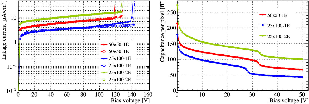
FIGURE 6. SINTEF 3D diode measurements performed on wafer at the end of the process on the final metal. I-V (Left) and C-V (Right) curves are shown. A systematic uncertainty, not shown in the figures, of less than 10% has been estimated for both current and capacitance measurements, due to temperature variations and the LCR circuit, respectively. The systematic uncertainties due to the test instrument for the considered voltage and current range are smaller than 1%.
5 Bump Bonding and Assembly
As mentioned above, the final 3D sensors will be read out by the ITkPix front end. Since this chip is not yet available, the results of RD53A prototypes will be presented. Each pixel of the 3D sensors is connected to the corresponding readout channel of the RD53A chip through a process called bump-bonding. The process consists in depositing a metal layer on top of ASIC and sensor pads (Under Bump Metallization or UBM) followed by solder balls (SnAg, SnPb, or Indium). Then the devices are interconnected through a thermal compression cycle called flip-chip.
The wafers of FBK second and third batches were sent for hybridization to the Leonardo Company (Rome, Italy) which performed electroplating UBM and bump-bonding to RD53A chips with Indium bumps. Wafers from the SINTEF run 4 were instead processed at IZM (Berlin, Germany) and flip-chipped to RD53A chips with solder bumps (SnAg). Also in the case of CNM sensors, RD53A chips with solder bumps were used, but the run 9761 was processed with electroless UBM at CNM, and flip-chipped at IFAE, while the run 11119 was sent to IZM, processed with standard electroplated UBM and flip-chipped partially at IZM and partially at IFAE. For module testing, the assemblies are then attached and wire-bonded to a dedicated PCB designed by the University of Bonn.
6 Irradiation
The spectrum of particles expected in the ITk pixel detector consists mostly of charged hadrons (more than 80%) and, in particular, it is dominated by pions. Other contributions coming from neutral hadrons, electrons, positrons, muons and photons are minor. Presently none of the existing irradiation facilities is able to offer a pion beam with sufficient flux to reach the required high doses in a reasonable time. Nevertheless, many facilities offer proton beams with energies ranging from tens of MeV up to GeV which enable to study the radiation hardness of sensors in terms of damage caused by both Non-Ionizing Energy Loss (NIEL) and Total Ionizing Dose (TID) effects.
Proton beams with relatively low energies have been employed for RD53A module irradiation in three different facilities: at the cyclotron of the Karlsruher Institut für Technologie (KIT) in Germany where 23 MeV protons are provided; at the Medical Physics cyclotron of the University of Birmingham in the UK with proton beams of approximately 27 MeV; and at the Cyclotron Radio Isotope Center (CYRIC) of the Tohoku University in Japan using 70 MeV protons. In all these facilities, during irradiation, the modules are kept at temperatures below 0°C and the beam is moved over the sensor surface to obtain a uniform dose. Irradiations to reach the final target fluence of
More RD53A modules have been irradiated with a 23 GeV proton beam from the PS accelerator at the IRRAD facility of CERN. The high energy of the particles provided by this facility allows irradiation of several modules at the same time and reaches directly the target fluence of
Irradiations have also been performed with neutrons in the TRIGA Mark II research reactor of the Jožef Stefan Institute (JSI) in Ljubljana, Slovenia. The neutron reactor allows investigation of only the NIEL damage since the TID due to gamma emission is very low, about 0.1 Mrad per
A summary of the RD53A modules employed for the following studies and their corresponding irradiation history can be found in Table 1. For proton irradiation, the dose received and the corresponding equivalent neutron fluence are measured from the activation of an aluminum foil placed in front of the sensors during irradiation. In the case of neutron irradiation, it is instead extrapolated from the predicted neutron flux and the immersion time in the reactor. In both cases a systematic uncertainty of 10% is associated to the fluence values.
TABLE 1. List of RD53A 3D pixel module studied in laboratories and with beam test experiments.
7 Module Characterization
7.1 Electrical Properties
The leakage current is a basic property of silicon detectors that indicates their electrical quality. This has been measured as a function of the bias voltage for 3D diodes and 3D sensors bump-bonded to RD53A chips before and after irradiation. The 3D modules are kept at constant temperature and relative humidity of less than 50% within a climate chamber. Before irradiation the measurements are carried out at 20°C, while after irradiation the sensors are cooled down to −25°C. Diodes are measured in the same conditions either on a probe station with a temperature controlled chuck or on dedicated Printed Circuit Boards (PCBs) inside a climate chamber. Systematic uncertainties for the measurements of the leakage current are dominated by the variation of the temperature which is measured with a precision better than 1°C corresponding to an uncertainty on the measured leakage current of less than 10%.
The leakage current as a function of the bias voltage for CNM and FBK RD53A sensors with different pixel geometries is compared in the plots in Figure 7. The properties before irradiation are mostly consistent with the measurements at wafer level with the exception of a few sensors which show a degradation of the I-V curves both in terms of leakage current level and breakdown voltage.
FIGURE 7. I-V curves of RD53A modules before and after irradiation. On the left modules assembled with 3D sensors from the CNM run 9761. On the right modules assembled with 3D sensors of the FBK second and third batches.
After irradiation the leakage current increases with the fluence and the breakdown is usually shifted towards larger voltages. Most RD53A sensors measured after irradiation show a breakdown larger than 120 V, while for two sensors (one from CNM and one from FBK) the steep increase of the leakage current is observed between 50 and 100 V. Conversely, the other sensors show very similar electrical behaviors after irradiation despite their different I-V curves observed before irradiation. No significant difference is observed in the I-V of these modules, for different pixel cell geometries after similar irradiation levels.
To increase the statistical data set and understand the variability of the I-V characteristics after irradiation, several diodes from the FBK and CNM productions have been irradiated at JSI with neutrons. Only diodes that before irradiation met the specification set in Section 2.4 have been selected for this study. Their leakage current as a function of the bias voltage after irradiation up to
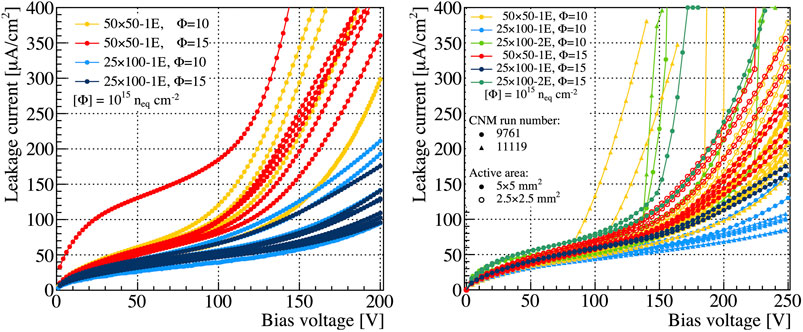
FIGURE 8. I-V curves of 3D diodes with different pixel geometries after neutron irradiation at JSI, Ljubljana. On the left diodes from the FBK second and third batches. On the right diodes from the CNM runs 9761 and 11119.
The different leakage current observed is consistent with the separation of the electrodes of the different pixel cell geometries that determines the strength of the electric field inside the active substrate. The diodes with the 25 × 100−2E pixel geometry show the highest leakage current levels and in many cases have a breakdown with a sudden increase of the current (hard breakdown) before reaching 250 V; the diodes with the 50 × 50−1E pixel geometry have lower currents, and in a few cases of the CNM production on Si-on-Si wafer (run 11119) a hard breakdown is observed at less than 250 V. Most of the CNM diodes have a smooth increase of the current (soft breakdown) around 150 V, which is consistent with the measurements on RD53A modules, while FBK diodes have a soft breakdown starting between 100 and 150 V; the 25 × 100−1E pixel geometry is the one showing the lowest current levels and better performance in terms of breakdown voltage both for FBK and CNM diodes. For this design no hard breakdown is observed in the measured diodes up to 250 V.
Only a small increase of the current can be seen between the diodes irradiated to
The larger current measured in the FBK diodes with respect to the CNM ones is consistent with the smaller dimensions of the former and the consequently larger fraction of the current coming from the edges with respect to that generated in the active area. A similar difference is observed on average between the two sizes of the 50 × 50−1E diodes of the CNM productions and with the RD53A sensors.
7.2 Beam Test Measurements
Pixel modules have been measured before and after irradiation in two different beam test facilities: at the Super Proton Synchrotron (SPS) of CERN using pions of 120 GeV and at the Deutches Electronen-Synchrotronen (DESY) in Hamburg with electrons of about 5 GeV [18]. In both cases a EUDET-type telescope [19] has been used to reconstruct the trajectories of the particles in the beam and determine the impact point on the studied devices (Detectors Under Test or DUT). The telescope has two arms, each one consisting of three planes made of MIMOSA26 [20] monolithic sensors with an active area of 2 × 1 cm2, and can provide a pointing resolution of up to 2 µm depending on the beam energy, the amount of material between the telescope planes and the consequent multiple scattering. The coincidences of up to four scintillators placed at the two ends of the telescope and covering the MIMOSA26 sensor area are used to generate the trigger signal for the readout. The DUTs are placed between the two arms of the telescope inside a cooling box. At SPS a custom designed cooling box based on a commercial chiller allows the DUT to reach temperatures as low as -50°C to study irradiated modules, as well as to keep a constant temperature of 20°C for the operation of non-irradiated modules. The same solution could not be used at DESY due to the lower particle energy and the large mass of the chiller-based box which would lead to a significant amount of multiple scattering. In this facility a lightweight Styrofoam box is used instead. Here cooling for operations with irradiated modules is provided by dry ice which allows them to reach temperatures as low as the chiller-based box, but without the flexibility of a precise temperature control. Two different data acquisition systems (DAQ) have been used to equalize the threshold and operate the RD53A chips: the BDAQ53 [21] developed by the Bonn Silicon Laboratory and the YARR system developed at LBNL [22]. Due to the large integration time of the MIMOSA26 sensors (about 300 µs) with respect to the DUTs (of the order of 25 ns), an additional reference plane made of a hybrid module composed of an FE-I4 chip and a planar sensor is used to provide timing information for track selection with 25 ns precision. In Table 1 are listed the sensors that have been investigated with particle beams at beam tests.
7.2.1 Hit Efficiency
The hit efficiency is defined as the fraction of events in which a particle passing through the active part of the DUT causes a recorded hit. Hence, it is highly influenced by the number of electron-hole pairs generated (proportional to the active thickness) and the chip threshold settings. The minimum hit efficiency target for ITk is 97% throughout the whole lifetime since lower values would cause problems for track pattern recognition [23]. Experimentally, the efficiency is determined in beam tests by extrapolating the reference track position to the DUT and searching for a hit cluster in the surroundings within a matching distance of up to two times the DUT pixel size. To disentangle the performance of the sensor from the one of the RD53A chip and from the hybridization process, noisy as well as disconnected channels are excluded from the efficiency calculation.
Results of hit efficiency measured as a function of the bias voltage are shown in Figures 9, 10 and 11 for RD53A chip modules with sensors produced by CNM, FBK and SINTEF, respectively.
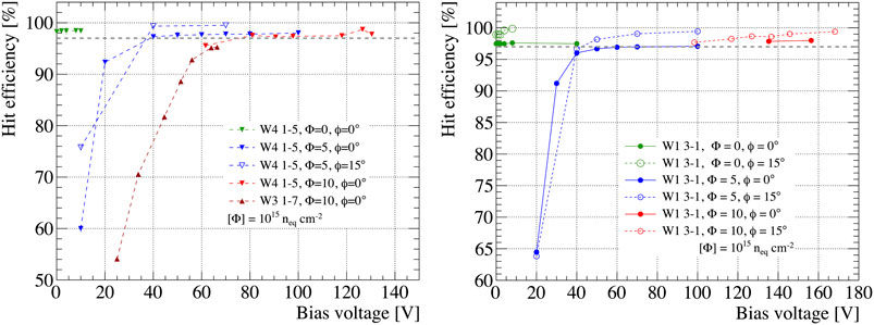
FIGURE 9. Hit efficiency as a function of the bias voltage for RD53A modules with CNM 3D sensors from run 9761 before and after irradiation. On the left (right) results of sensors with 50 × 50−1E (25 × 100−1E) pixel geometry obtained with the Differential (Linear) front-end are shown. The BDAQ readout system has been used for tuning and data-taking. The modules are tuned to a mean threshold of 1 ke. A systematic uncertainty of 0.3% is associated to all efficiency measurements. Partially adapted from Reference [25, 26].
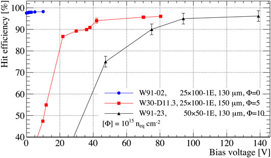
FIGURE 10. Hit efficiency as a function of the bias voltage for RD53A modules with FBK 3D sensors from second and third batches before and after irradiation. The modules are tuned to a mean threshold of 1 ke.
FIGURE 11. Hit efficiency as a function of the bias voltage for RD53A modules with SINTEF 3D sensors from run four before and after irradiation. The sensors have a 50 × 50−1E pixel geometry. For better visibility the data of D61-2 before irradiation (black circles) is shifted by −1 V.
7.2.1.1 Before Irradiation
Before irradiation sensors with both 50 × 50 and 25 × 100 µm2 pixel cell geometries show a hit efficiency over 97% for perpendicularly incident tracks even with a bias of 0 V. Differences of less than 1% efficiency have been observed for threshold tunings between 1.0 and 1.5 ke and in results obtained for sensors produced by different foundries on substrate thicknesses from 100 to 150 µm. For the 50 µm thick SINTEF sensors similar results are obtained with a threshold of 500 e which could be achieved thanks to the lower pixel capacitance. Inefficiencies mainly correspond to particles crossing the fully passing p-type columns which are inactive as can be appreciated looking at the efficiency distribution over one pixel cell shown in Figure 12. Indeed, the efficiency increases to over 99% when the sensors are tilted by 15° as it is possible to see from the results of RD53A modules using CNM 3D sensors in Figure 9. In this case the efficiency distribution over the pixel cell is uniform since the particles are not passing all the way through the p-columns.
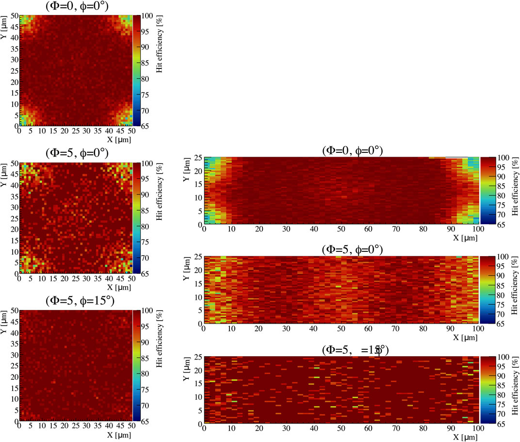
FIGURE 12. Hit efficiency over the surface of one pixel cell with 50 × 50−1E (left) and 25 × 100−1E (right) geometries [25]. From top to bottom the maps show modules measured before irradiation at perpendicular beam incidence (
7.2.1.2 After Irradiation
Results of RD53A modules with 50 × 50−1E sensors from all three production sites have demonstrated the possibility of reaching a hit efficiency larger than 96% for perpendicularly incident tracks after irradiation to
The 25 × 100−1E sensor from CNM after irradiation to a particle fluence of
These results are also compatible with FBK modules coming from the second batch production and measured by the CMS Collaboration [24], where an efficiency close to 97% was obtained for both 50 × 50−1E and 25 × 100−1E modules operated at 150 and 120 V, respectively.
The hit efficiency results of the different modules and productions can be considered to be consistent within the tuning uncertainties (
7.3 Charge Sharing and Cross-Talk
Cross-talk and in general larger charge sharing has been observed in 25 × 100−1E sensor prototypes before irradiation. The cross-talk threshold, defined as the average charge injected in a pixel for which a hit is observed in a neighboring pixel, has been measured on FBK RD53A modules and is shown in Figure 13. In the 25 × 100−1E design cross-talk thresholds between 12 and 25 ke have been measured by injecting one pixel and reading out the pixels adjacent to the 100 µm sides. In the 50 × 50−1E design a cross-talk threshold of about 150 ke has been estimated by injecting the four neighboring pixels at the same time and scaling the result. A larger charge sharing in the 25 × 100−1E design with respect to the 50 × 50−1E design has been observed also in beam test measurements with CNM sensors. Before irradiation about 50% of the perpendicular incident tracks passing through the 25 × 100−1E sensor resulted in a cluster size larger than 1, while only 20% have this characteristic in the 50 × 50−1E sensor. After irradiation the charge sharing is mostly suppressed and for both designs the number of clusters with a size larger than 1 is lower than 20% at perpendicular track incidence. This level of cross-talk and charge sharing is not considered critical for the readout and occupancy of the ITk innermost layer.
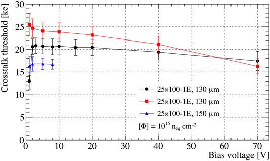
FIGURE 13. Cross-talk threshold as a function of the bias voltage for RD53A modules with 25 × 100−1E FBK sensors with different thickness (second and third batches).
8 Power Dissipation
Figure 14 shows the power dissipation of RD53A modules and diodes after irradiation. The curves are calculated from the I-V characteristics presented in Section 7.1. The annealing times of the modules before the I-V was measured are of the order of 3–4 days. The diodes have been instead irradiated with neutrons up to
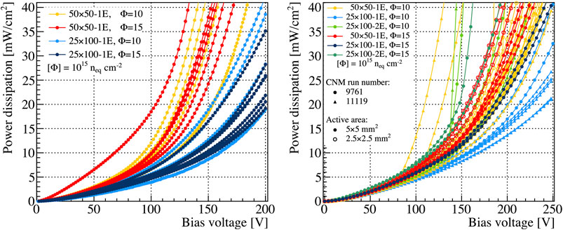
FIGURE 14. Power dissipation as a function if the bias voltage for FBK diodes (left) and CNM diodes (right) with different pixel geometries after neutron irradiation at JSI, Ljubljana.
9 Conclusions
Novel 3D pixel sensor prototypes featuring small pixel cells and thin active substrates have been produced at FBK, CNM, and SINTEF using a single-side approach. These sensors have been assembled with the new RD53A readout chip and evaluated to instrument the innermost pixel layer of ITk. Results showed that these sensors meet the ITk specifications before irradiation in terms of capacitance, depletion voltage and leakage current. After irradiation up to
Data Availability Statement
The raw data supporting the conclusions of this article will be made available by the authors, without undue reservation.
Author Contributions
The article has been written by ST with contributions from SG (Chapters 1 and 2), GP (Chapter 4.1), G-FDB (Chapters 3 and 4.2) and MP (Chapter 4.3). Design, manufacturing and measurements at wafer level of CNM and SINTEF sensors have been performed by the CNM group (GP, MM, and DQ) and the SINTEF group (AK, OK, and MP), respectively. The design of FBK sensors has been done by G-FDB and RM, while manufacturing and measurements at wafer level have been performed by the FBK group (MB, FF, RM, and SR). Characterization at beam test and in the laboratory, and analysis of the data of diodes and RD53A modules have been performed by the IFAE group (JC, GGi, SG, and ST), the Genova and Trento groups (G-FDB, GD, GGa, CG, AL, HO, MS, and LV), and the Oslo and Bergen groups (OD, AH, SH, ML, OR, HS, and BS) for CNM, FBK and SINTEF sensors, respectively. All authors contributed to the article and approved the submitted version.
Funding
This work was partially funded by: MINECO, Spanish Government, under grants RTI2018-094906-B-C21, RTI2018-094906-B-C22 and SEV-2016-0588 (Severo Ochoa excellence programme); the Italian National Institute for Nuclear Physics (INFN), Projects RD_FASE2 and FASE2_ATLAS (CSN1); and by the H2020 project AIDA-2020, GA no. 654168.
Conflict of Interest
The authors declare that the research was conducted in the absence of any commercial or financial relationships that could be construed as a potential conflict of interest.
The reviewer SS declared a past collaboration with one of the authors GB to the handling editor.
Acknowledgments
The authors would like to thank A. Rummler, M. Bomben, J. Lange and the other ATLAS ITk beam test participants for great support and discussions at the beam test as well as A. Dierlamm and F. Bögelspacher (KIT), K. Nakamura (CYRIC), L. Gonella and A. Hunter (University of Brimingham), V. Cindro (JSI) for the excellent support with the irradiation at the different facilities. The measurements leading to these results have been partially performed at the Test Beam Facility at DESY Hamburg (Germany), a member of the Helmholtz Association (HGF).
References
1. Capeans M, Darbo G, Einsweiller K, Elsing M, Flick T, Garcia-Sciveres M, et al. (2010). ATLAS Insertable B-Layer technical design report. Tech rep CERN. CERN-LHCC-2010-013.
2. Grinstein S, Cavallaro E, Chmeissani M, Dorholt O, Förster F, Lange J, et al. Module production of the one-arm AFP 3D pixel tracker. JINST (2017) 12:C01086. doi:10.1088/1748-0221/12/01/C01086
3. Aad, G. , Butterworth, J.M. , Thion, J. , Bratzler, U. , Ratoff, P.N. , Nickerson, R.B. , Seixas, J.M. The ATLAS experiment at the CERN large hadron collider. JINST (2008) 3:S08003. doi:10.1088/1748-0221/3/08/s08003
4. Garcia-Sciveres M. The RD53A integrated circuit. Tech Rep CERN-RD53-PUB-17-001 (2017). CERN-RD53-PUB-17-001.
5. Da Via C, Boscardin M, Dalla Betta GF, Darbo G, Fleta C, Gemme C, et al. 3D silicon sensors: design, large area production and quality assurance for the ATLAS IBL pixel detector upgrade. Nucl Instrum Meth A (2012) 694:321–330. doi:10.1016/j.nima.2012.07.058
6. Da Via C, Watts SJ. The geometrical dependence of radiation hardness in planar and 3D silicon detectors. Nucl Instrum Meth A (2009) 603:319–324. doi:10.1016/j.nima.2009.02.030
7. Pellegrini G, Lozano M, Ullán M, Bates R, Fleta C, Pennicard D. First double-sided 3-D detectors fabricated at CNM-IMB. Nucl Instrum Meth A (2008) 592:38–43. doi:10.1016/j.nima.2008.03.119
8. Pennicard D, Pellegrini G, Lozano M, Bates R, Parkes C, Wright V. Simulation results from double-sided 3d detectors. IEEE Nucl Sci Symp Conf Rec (2006) 3:1614–8. doi:10.1109/NSSMIC.2006.354206
9. Pellegrini G, Garcia F, Balbuena J, Cabruja E, Lozano M, Orava R, et al. Fabrication and simulation of novel ultra-thin 3D silicon detectors. Nucl Instrum Meth A (2009) 604:115–8. doi:10.1016/j.nima.2009.01.039
10. Pellegrini G, Manna M, Quirion D, 3D-Si single sided sensors for the innermost layer of the ATLAS pixel upgrade. Nucl Instrum Meth A (2019) 924:69–72. doi:10.1016/j.nima.2018.05.076
11. Baselga M, Pellegrini G, Quirion D, Simulations of 3D-Si sensors for the innermost layer of the ATLAS pixel upgrade. Nucl Instrum Meth A (2017) 847:67–76. doi:10.1016/j.nima.2016.11.033
12. Zoboli A, Boscardin M, Bosisio L, Dalla Betta G, Piemonte C, Ronchin S, et al. Double-sided, double-type-column 3-D detectors: design, fabrication, and technology evaluation. IEEE Trans Nucl Sci (2008) 55(5):2775–84. doi:10.1109/TNS.2008.2002885
13. Giacomini G, Bagolini A, Boscardin M, Dalla Betta G, Mattedi F, Povoli M, et al. Development of double-sided full-passing-column 3D sensors at FBK. IEEE Trans Nucl Sci (2013) 60(3):2357–66. doi:10.1109/TNS.2013.2262951
14. Dalla Betta GF, Boscardin M, Darbo G, Mendicino R, Meschini M, Messineo A, et al. Development of a new generation of 3D pixel sensors for HL-LHC. Nucl Instrum Meth A (2016) 824:386–7. doi:10.1016/j.nima.2015.08.32
15. Sultan D, Dalla Betta GF, Mendicino R, Boscardin M, Ronchin S, Zorzi N, First production of new thin 3D sensors for HL-LHC at FBK. JINST (2017) 12:C01022. doi:10.1088/1748-0221/12/01/C01022
16. Oide H, Alimonti G, Boscardin M, Betta GFD, Darbo G, Ficorella F, et al. INFN-FBK developments of 3D sensors for High-Luminosity LHC. Nucl Instrum Meth A (2019) 924:73–7. doi:10.1016/j.nima.2018.10.022
17. Mandic I, Cindro V, Kramberger G, Kristof ES, Mikuz M, Vrtacnik D, et al. Bulk damage in DMILL npn bipolar transistors caused by thermal neutrons versus protons and fast neutrons. IEEE Transaction Nucl Sci (2004) 51:1752–8. doi:10.1109/TNS.2004.832927
18. Diener R, Dreyling-Eschweiler J, Ehrlichmann H, Gregor I, Kotz U, Krämer U, et al. The DESY II test beam facility. Nucl Instrum Meth A (2019) 922:265–86. doi:10.1016/j.nima.2018.11.133
19. Rubinskiy. I. An EUDET/AIDA pixel beam telescope for detector development. Phys Proc (2012) 37:923. doi:10.1016/j.phpro.2012.02.434
20. Hu-Guo C, Baudot J, Bertolone G, Besson A, Brogna AS, Colledani C, et al. A ten thousand frames per second readout MAPS for the EUDET beam telescope. Tech rep CERN (2009). doi:10.5170/CERN-2009-006.47
21. Daas M, Dieter Y, Dingfelder J, Frohne M, Giakoustidis G, Hemperek T, et al. BDAQ53, a versatile pixel detector readout and test system for the ATLAS and CMS HL-LHC upgrades. Nucl Instrum Meth A (2020) 986:164721. doi:10.1016/j.nima.2020.164721
22. Heim T. Yarr - a PCIe based readout concept for current and future ATLAS pixel modules. J Phys Conf Ser (2017) 898:032053. doi:10.1088/1742-6596/898/3/032053
23.ATLAS Collaboration. Technical design report for the ATLAS inner tracker pixel detector. Tech rep CERN (2017). CERN-LHCC-2017-021.
24. Alonso AG, Currás E, Duarte-Campderrós J, Fernandez M, Gomez G, Gonzalez J, et al. Test beam characterization of irradiated 3D pixel sensors. JINST (2020) 15:C03017. doi:10.1088/1748-0221/15/03/C03017
25. Terzo S, Chmeissani M, Giannini G, Grinstein S, Manna M, Pellegrini G, et al. Performance of irradiated RD53A 3D pixel sensors. JINST (2019) 14:P06005. doi:10.1088/1748-0221/14/06/p06005
Keywords: solid state detectors, radiation-hard charged-particle detectors, 3D silicon detectors, tracking detectors, ATLAS experiment, high energy physics (HEP)
Citation: Terzo S, Boscardin M, Carlotto J, Dalla Betta G-F, Darbo G, Dorholt O, Ficorella F, Gariano G, Gemme C, Giannini G, Grinstein S, Heggelund A, Huiberts S, Kok A, Koybasi O, Lapertosa A, Lauritzen ME, Manna M, Mendicino R, Oide H, Pellegrini G, Povoli M, Quirion D, Rohne OM, Ronchin S, Sandaker H, Abdulla Samy MA, Stugu B and Vannoli L (2021) Novel 3D Pixel Sensors for the Upgrade of the ATLAS Inner Tracker. Front. Phys. 9:624668. doi: 10.3389/fphy.2021.624668
Received: 31 October 2020; Accepted: 04 January 2021;
Published: 21 April 2021.
Edited by:
Andrei Nomerotski, Brookhaven National Laboratory (DOE), United StatesReviewed by:
Peter R. Hobson, Queen Mary University of London, United KingdomSally Seidel, University of New Mexico, United States
Copyright © 2021 Terzo, Boscardin, Carlotto, Dalla Betta, Darbo, Dorholt, Ficorella, Gariano, Gemme, Giannini, Grinstein, Heggelund, Huiberts, Kok, Koybasi, Lapertosa, Lauritzen, Manna, Mendicino, Oide, Pellegrini, Povoli, Quirion, Rohne, Ronchin, Sandaker, Abdulla Samy, Stugu and Vannoli. This is an open-access article distributed under the terms of the Creative Commons Attribution License (CC BY). The use, distribution or reproduction in other forums is permitted, provided the original author(s) and the copyright owner(s) are credited and that the original publication in this journal is cited, in accordance with accepted academic practice. No use, distribution or reproduction is permitted which does not comply with these terms.
*Correspondence: Stefano Terzo, c3RlZmFuby50ZXJ6b0BjZXJuLmNo