 Paolo Conci1
 Giovanni Darbo2*
 Andrea Gaudiello2,3
 Claudia Gemme2Stefano Girardi4
 Alessandro Lapertosa2,3Francesca Mattedi1
 Alessio Volpe2
- 1MicroFabSolutions s.r.l, Trento, Italy
- 2INFN Sezione di Genova, Genova, Italy
- 3Dipartimento di Fisica, Università di Genova, Genova, Italy
- 4FBK–Fondazione Bruno Kessler, Trento, Italy
Pixel technology is commonly used in the tracking systems of High Energy Physics detectors with physical areas that have largely increased in the last decades. To ease the production of several square meters of sensitive area, the possibility of using the industrial Wafer Level Packaging to reassemble good single sensor tiles from multiple wafers into a reconstructed full wafer is investigated. This process reconstructs wafers by compression molding using silicon charged epoxy resin. We tested high glass transition temperature low-stress epoxy resins filled with silica particles to best match the thermal expansion of the silicon die. These resins are developed and characterized for industrial processes, designed specifically for fan-out wafer-level package and panel-level packaging. In order to be compatible with wafer processing during the hybridization of the pixel detectors, such as the bump-bonding, the reconstructed wafer must respect challenging technical requirements. Wafer planarity, tile positioning accuracy, and overall thickness are amongst the main ones. In this paper the description of the process is given and preliminary results on a few reconstructed wafers using dummy tiles are reported. Strategies for Wafer Level Packaging improvements are discussed together with future applications to 3D sensors or CMOS pixel detectors.
Introduction
Pixel detectors have been being used in HEP for thirty years [1]. The typical module design uses so-called hybrid detectors, where single readout chips are mated by a flip-chip process to silicon sensors and the electrical connection between the two parts is achieved thanks to bumps deposited on the wafers before the parts dicing. As the readout chip is limited in size by the technology used for its fabrication and such size is typically given by the maximum reticle dimension of few square centimeters, the detector module is usually assembled with a single sensor tile mated to an array of readout chips. The sub-micron precision of the sensitive pixel sensor is given by the fact that the sensor is a unique tile built using microelectronics lithography.
Traditionally, the sensors used in HEP have been based on the planar technology but in the last decade, new technologies have been developed to deal with the new challenges in the possible applications. To improve the radiation hardness performance of the pixel detectors, 3D sensors have been developed as an alternative to planar sensors [2, 3]. The technology to produce 3D sensors is much more complex and brings a lower yield with respect to the planar technology. For this reason, the 3D sensor are produced in smaller tiles, and this reflects into single-chip modules. The lower yield of 3D, respect to conventional planar technology, and single-chip module design have two disadvantages. First, the larger cost of bump-bonding, since more wafers must be processed for bump deposition and/or metallurgy preparation. Second, the higher number of smaller modules needed to cover the sensitive area in the experiment. A larger number of modules reflects, in turn, into a larger number of high energy particle tracks to be used for relative alignment. Another pixel sensor technology that is emerging in recent years is the active CMOS sensor, which is made either as a hybrid sensor (coupled with a readout chip) [4] or in the monolithic form [5]. This type of detector, which uses active components both for reading and sensing, is limited in size being based on submicron processes used for integrated circuits.
To overcome the above limitations, we have investigated the possibility to use industrial Wafer Level Packaging (WLP) to reassemble good single sensor tiles from multiple wafers into a reconstructed full wafer. In the following, we will refer to this new wafer as WLP. The WLP can then be diced into larger tiles grouping together several of the original ones, thus mimicking a larger single sensor tile. The technology process described in this paper uses a low-stress epoxy resin charged with silica. This commercial resin is used in industrial WLP processes and is known to be compatible with electronic circuits. Moreover, being an epoxy, it should be radiation tolerant to high levels. Its relatively high operating temperature makes it compatible with the indium bump-bonding thermal compression process that is limited to 100°C [6, 7].
WLP process is an advanced trend in electronics industrial packaging that is often combined with other technologies like redistribution layers (RDL) and through-strata-via (TSV) [8], largely used in sectors of mobile, high-performance computing, automotive (especially self-driving car), Internet of things (IoT), and Big Data (especially for cloud computing) [9, 10]. Similarly, if WLP was used for pixel detectors, post metallization could be used for fan-out purposes (FOWLP - Fan Out WLP) or RDL in signal and power routing. Selective etching could be used to open holes in the resin to contact the metal on the back of the sensor to carry the voltage bias. Additional services such as cooling channels can be integrated into the module by inserting them into the resin with special molds.
Preliminary studies were carried out with silicon dummy-sensors of 2 × 2 cm2 area and 300 µm thickness. The aim of this test was to study the WLP deformation and positioning accuracy of the dies, knowing that both are fundamental for the WLP process. We also carried out some preliminary investigations to reduce the overall thickness of the reconstructed wafer, since the application in the field of pixel sensors requires to keep the material budget to a minimum to reduce the secondary interaction or multiple scattering in the detector.
We describe in Description of the WLP Process the process that we set up and in WLP Mechanical and Geometrical Measurements the geometrical measurements on the reconstructed wafers. Finally, in Discussion of Results and Room for Improvements the results obtained compared to the requirements for pixel detector modules and the possibilities for improvements are discussed.
Description of the WLP Process
The WLP process was developed using the instrumentation for a wafer manufacturing line that MicroFabSolutions1 has access to in FBK2 (Trento). For this test we produced six 6-inch silicon wafers, 300 µm thick, with 24 dummy chips each, made with a single layer of metal. The metal pattern of each chip is very simple: four corners alignment crosses with 80 µm dicing streets for cutting into 2 × 2 cm2 dies. These wafers are cut into 24 dies (dummy chips) each and these parts are used for the rebuilding of the wafer using a mold and resin.
Another two 6-inch wafers, 675 µm thick, with a similar layout of die’s matrix, but with dies spaced 400 μm, have been made to use as WLP carrier wafers. If we consider that the dicing saw eats up approximately 50/60 µm of silicon of the dicing street, with the chosen placement distance between dies on the carrier wafer, we expect a gap of 360/370 µm in between dies. We have chosen such a value for two reasons: it is a kind of standard in today's pixel detectors and is big enough to be filled with the resin during the molding process.
The six wafers have been diced to use as parts for WLP and with them we have produced six WLPs having three different nominal thicknesses: 675, 450, and 300 µm. For the thickest ones we have used the full depth of the mold cavity of ∼1.5 mm. For the other WLP thicknesses we have added 6-inch wafers (spacer wafers), respectively of 275 and 450 μm, at the bottom of the cavity to reduce the space left for the resin. For each of the three thicknesses, we have made preliminarily a partially loaded wafer (cross-type) with 10 dies and then a fully loaded one (matrix-type), with 32 dies (see Figure 1 and Table 1).
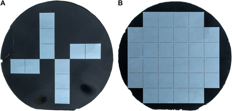
FIGURE 1. photos of WLP 5 “cross-type” (A) and WLP 6 fully loaded “matrix-type” (B) die placement.
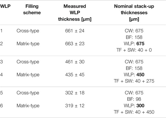
TABLE 1. Properties of the six WLP wafers produced by MicroFabSolutions together with the nominal values of the stack-up parts. In the “nominal thickness” column is given the full stack put into the mold cavity: Carrier Wafer (CW), Teflon Film (TF), Bonding Film (BF), dies plus resin (WLP), Spacer Wafer (SW).
Process Flow
The process flow, shown in Figure 2, consists of six steps:
1. Laminate carrier. A carrier wafer, used for chip placement, is inserted into the upper shell of the WLP mold and is laminated with the transparent bonding film. The part of the film that protrude from the carrier wafer is applied to the edge of the mold as shown in Figure 3A. The foaming adhesive side of the bonding film is in contact with the carrier wafer. The protective liner film is then removed.
2. Pick and Place. The mold with the carrier wafer is placed on the flip-chip machine. Dummy chips are picked and placed face down by sticking them to the bonding film. Dummy chips are aligned by matching the markers on the chips with the corresponding markers, visible through the bonding film, on the carrier wafer (Figure 3B).
3. Molding. A thin Teflon film of 40 µm is placed on the surface of the lower mold shell and then the resin is distributed uniformly in its whole cavity. The needed quantity of resin is controlled by a weight scale (Figure 3C). The two mold shells are clamped together and placed in the wafer bonder. The resin is degassed and preheated at 100°C to increase flowability. A compression force of 15,000 N is applied then and the resin cured at 130°C for 10 min. Finally, it is cooled down, force is released and the mold is extracted from the wafer bonder.
4. Release from bonding film. The mold is opened (Figure 3D) and the upper shell is put in an oven at 190°C for 10 min for foaming the foil adhesive of the bonding film. Then, the WLP is separated from the carrier wafer. The release force is very low due to the foam generated from the adhesive. The bonding film is on the WLP after this step of the process.
5. Peel-off bonding film. The bonding film is peeled-off from the WLP.
6. WLP–Wafer Level Package. The WLP is now ready and is easily extracted from the lower mold shell since the Teflon film avoids that the resin adheres to the aluminum surface of the mold.
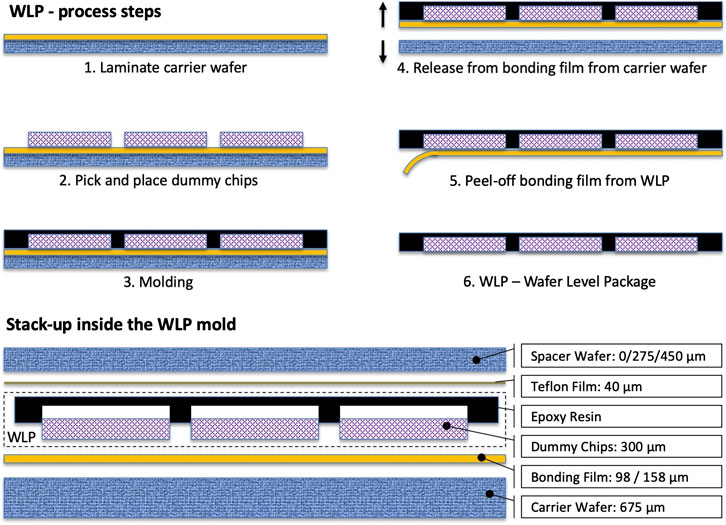
FIGURE 2. Top: the six steps of WLP process flow. Bottom: the complete stack-up present in the mold.
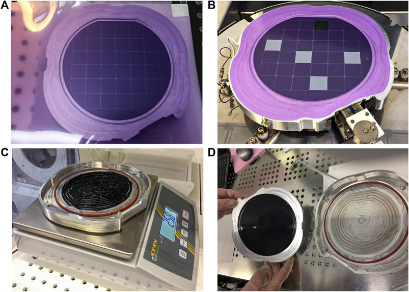
FIGURE 3. (A) lamination of the support wafer with the bonding film; (B) four dies placed on carrier wafer with flip-chip machine; (C) epoxy deposited in the bottom mold shell and weighting; (D) opened mold at the end of the process with the WLP to be extracted from the upper mold shell.
Experimental Process Test, Instruments and Materials
The WLP application in pixel detectors has few critical parameters that we tried to optimize with the selection of proper materials and procedures. In the final application we aim to assemble sensor parts very tight together at minimum achievable distance of typically 100/300 µm. This distance is much smaller than the one typically used in industrial microelectronics. Smaller distance should be an advantage for minimizing the displacement from original placement position due to the different CTE of resin with respect to silicon [11]. Instead, large silicon chips and mismatch CTE between silicon and resin could contribute to the deformation of the WLP due to the layering of the two materials. This is especially true with thicker resin [12].
Here below, we briefly describe the critical aspects in the process that we tried to mitigate with the selection of material and procedures.
Mold
We have made the mold in aluminum with a milling machine. Due to the limited space of the gap in the wafer bonder (8 mm), the mold is thin (2 mm in the thinnest parts of both upper and lower shell) and could deform under pressure. Moreover, it is difficult to mill with high precision aluminum. We are not able to evaluate how much the mold deformation may have influenced the warpage of the reconstructed wafer. Moreover, due to excessive cost, we have discarded in this test phase a mold made of a harder material and better mechanical precision.
Bonding Film
The used bonding film has thermal foaming adhesive on the side applied to the carrier wafer, while the other face has a an adhesive with relatively low peeling force. The thermal release happens when heated at 185/190°C for 30 s. The heating process generates foam that easily separates the carrier wafer from the WLP. The bonding film left on the WLP is removed by peeling off.
For the first four wafers, we used a foaming sheet that was very difficult to peel-off from the WLP side, and in one case a wafer even broke down. In the wafers made with this film, we noticed, after removing the film, slight wrinkles on the surface corresponding to the inter-chip position. We think that this was due to the excessive peel-off force. Parts of the film remained on the WLP and we had to use chemicals solvents to remove them completely.
For the last two wafers, we used a different film, ICROS™3 film, which has a very low peel-off force and was very easy to remove from the WLP without producing any mechanical damage.
Both bonding films have good transparency and a total thickness (film + adhesive) of 100/150 µm allowing the placement with the flip-chip machine.
Resin
Our goal is to achieve the minimum thickness of resin. Ideally, we would like to have the same total WLP thickness as the sensor thickness, and this goes into the direction of minimizing the warpage. We also selected a resin with a relatively low CTE that reduces the effect of expansion/contraction during the molding and subsequent curing thermal processes. Resins that best match silicon CTE usually have a high percentage (90%) of silica filler. Resins with a high percentage of filler use relatively large size particles (35 µm). For our application, which requires very little resin thickness over dies, we had to compromise CTE amongst filler size.
In the considered applications for pixel detector, we have to perform a series of mechanical or chemical operations on WLP’s and some of them need thermal processes. For instance, the bump-bonding of sensor and front-end readout chip for hybrid pixel detectors uses thermal compression at 100°C of indium bumps to make the connections.
In addition, we paid attention to the initial distribution of the resin and selected a high flowable one to minimize the drag force on the placed chips during compression.
Considering the previous requirements, we chose the epoxy/amine resin XV5791S14 from Panasonic4 [13], specifically designed for FOWLP and having high Tg (glass transition temperature) and low-stress performance. Table 2 summarizes the main proprieties of the resin.
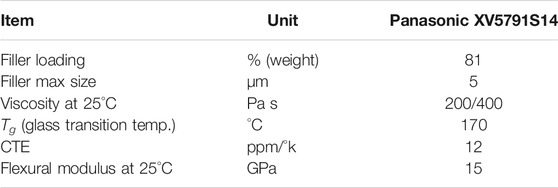
TABLE 2. material parameters of the Panasonic XV5791S14 epoxy/amine resin.
Dummy chips are placed face down (see Figure 3B) on the carrier wafer using a flip-chip machine with a nominal positioning accuracy of 10 μm; today an upgraded machine with an accuracy di 1 µm would be available. The reference crosses on the dummy chips are superimposed to the corresponding ones on the carrier wafer with the manual alignment provided by the flip-chip machine. Since the dies are placed facing down, the positioning of the placement cannot be verified directly but must rely on the accuracy and calibration of the flip-chip.
The final accuracy in die placement depends not only on the initial placement, but also on other effects that could affect the final results. The main effects and actions to mitigate them are:
1. Pick and Place initial positioning error – machine upgrade with 1 µm precision;
2. Resin flow resisting force on chips during the molding process – low viscosity, preheating before applying compression;
3. thermal expansion/contraction during the molding/hardening process – low CTE resin;
4. thermal contraction during the epoxy curing process;
5. thermal contraction during the debonding process from the support carrier.
Extraction From the Mold and WLP Handling
We found no difficulties in extracting the WLP from the mold. The edge of several WLPs is not very sharp and slightly jagged as can be seen in Figure 1B. This is, at least in part, due to the resin escaping between the two mold shells. The first four WLPs have suffered the removal of the adhesive film as explained above and have some surface folds (wrinkles) along the chip separation lines (see Figure 4). The handling of the reconstructed wafers exhibits a brittleness similar to that of silicon wafers of equivalent thickness. WLP 5 broke into two parts during subsequent handling. WLP 6, the thinnest, has a thinner resin layer toward the outside of the wafer and this is clearly visible becoming semi-transparent and showing the back of the chips.
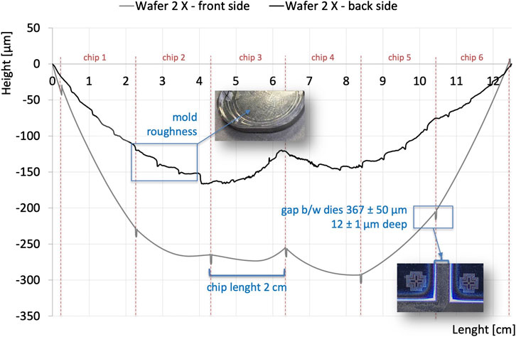
FIGURE 4. lower (gray) and upper (black) diametrical profile of WLP 2. In the profile of the upper side, the curvatures of the individual chips and the gaps not completely filled with resin are visible between one chip and the next. This is due to the protrusion of the bonding film between the chips after the application of the high pressure. The roughness of the mold machining is visible in the profile of the lower side. Between chip number three and four is visible the wrinkle described in the text.
WLP Mechanical and Geometrical Measurements
We used two different geometries to position the dies in the WLP (matrix-type or cross-type) and three different WLP’s thicknesses as summarized in Table 1. The two fill patterns were designed to further test the strength of the resin. WLPs 2, 4, and six have 32 tiles (matrix-type) while WLPs 1, 3, and five have 10 tiles (cross-type). The resulting WLP wafers are shown in Figure 1: the resin used in the epoxy molding compound is visible in black. The WLP target and measured thicknesses are in Table 1.
The thickness of the WLPs was reduced step-by-step, from 675 µm (1 and 2) to 450 µm (3 and 4) and finally to 300 µm (5 and 6) to confirm the strength of the compound. The first production includes 675 and 450 µm WLPs, which are tough enough to handle. Subsequent production includes two more WLPs with the minimum obtainable thickness, 300 µm as the dummy dies.
Planarity Measurement
The three matrix-type WLPs (2, 4, and 6) were measured to evaluate the flatness. Measurements were performed, with a KLA-Tencor5 P-7 stylus profiler, on the top side of the wafers (chip side). We measured eight profiles of 12.5 cm in length, 1 cm apart, in steps of 20 μm, both in the X and Y direction (see Figure 5). In Figure 5B we show the eight profiles along X for WLP 6. One of the profiles taken near the X diameter of the WLP is used to measure the bow of the 6 center chips as shown in Figure 5 and summarized in Table 3.
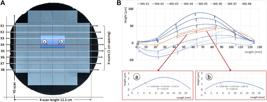
FIGURE 5. Eight 12.5 cm long profiles (X1-X8), distanced by 1 cm, were taken with a 20 µm step on WLP 6 along X direction (A) sketch of the wafer with the profiles highlighted (B) top, eight profiles after rotation; bottom, in red the X4 profile used to extract information on the warpage of the chips. The profiles are rotated and shifted to bind the two ends to have ordinates equal to zero.
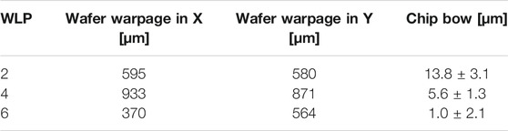
TABLE 3. Warpage of the WLP 2, 4 and 6 and bow of their chips.
To get an indication of the deformation of the WLP using the stylus profiler measurements, we reconstructed the 12.5 × 7 cm2 surface using the eight non-rotated profiles (X1, ..., X8) shown in Figure 5 and adding a vertical displacement given by a scan of profile Y0. The resulting surface, i.e., the matrix of discrete points, is fitted by a plane. The surface obtained by subtracting the plane from the original surface is plotted in the 2D and 3D views for WLP 6 in Figure 6. The warpage is obtained from the difference in the maximum and minimum Z value of that transformed surface. The warpage values for the three matrix-type WLPs are in Table 3. For comparison, we evaluated with the same method the warping by rotating the wafer by 90° and performing the scans and surface reconstruction as just described (see Table 3).
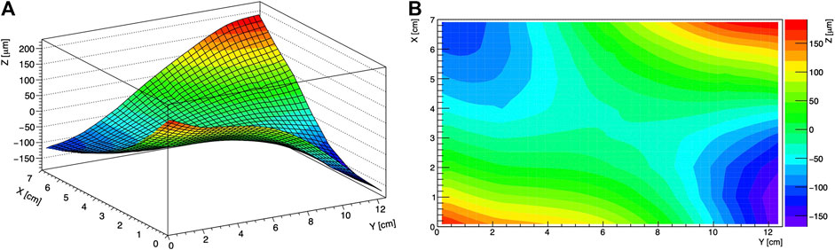
FIGURE 6. (A) 3D reconstruction and (B) 2D map of the surface of wafer six reconstructed combining eight profiles along X axis. The surface has been straightened up by subtracting a plane, previously fitted.
We must observe that WLP 2 and 4 have wrinkles along the seam lines between the chips, as can be seen in the profile of Figure 4. We believe they were generated during the peeling of the adhesive film. The second thing we need to point out is that the chip bow is maximum for the thickest WLP as we expect due to the thermal effect of the molding process and the mismatch in the resin and silicon CTE.
Placement Precision Measurement
The positioning accuracy was extracted as the spread of the distance distribution between the alignment crosses. The distance between the alignment crosses was measured with a Keyence VHX-100 microscope, along the X and Y directions for all available chips (see Figure 7).
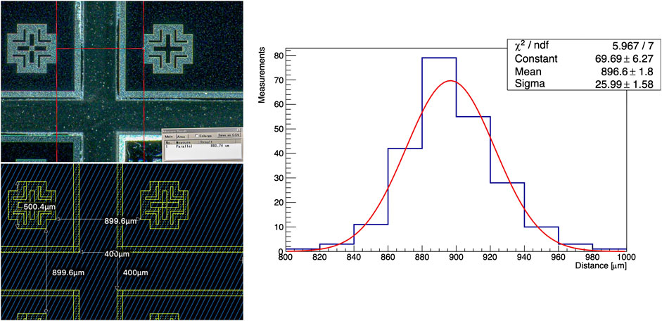
FIGURE 7. Left: alignment crosses between chips, the design distance is 900 μm; Right: fit to the total distribution of the distances between crosses in WLP 2, 4 and 6.
The design distance between crosses is 899.6 μm: this distance is used as a reference for the positioning of the chips, as the chips were positioned on top of a support wafer with the same crosses. The average distance measured on WLP 2, 4 and 6 is of 892 ± 27, 908 ± 33 and 890 ± 18 μm, respectively. The positioning accuracy can be extracted from a fit to the entire distance distribution in WLP 2, 4 and 6: an uncertainty of 26 μm can be assumed from the Gaussian sigma.
The placement accuracy observed is compatible with the precision of the flip-chip machine used by MicroFabSolutions for the placement of the tiles, considering that the optical system is affected by vision through the bonding film and chip are deposited on top of a soft material. This level of precision is enough for multi-chip module assembling. The design requirements for ATLAS ITk (Inner Tracker) of the phase II LHC update in the position accuracy of single-chip modules in a multi-module structure is 20 μm, which corresponds to 28 µm in distance distribution accuracy [14]. However, the accuracy achieved is not sufficient for photolithographic mask processes, for example, required to deposit indium bumps. An accuracy of ∼2 µm is required for this application, which could be achieved with a higher precision flip-chip machine.
Thickness Measurement
The WLP thickness was measured with a Mitutoyo digital micrometer, having an accuracy of 1 µm. Measurements were performed for matrix-type WLPs on the 16 chips that were reachable by the instrument (i.e. 4 chips per side, in the outer chip rows and columns). Similarly, in the same positions, the cross-type WLPs were measured.
The thickness measured per each wafer is reported in Table 2: the process helped to reach the target thickness within uncertainties. Wafer 6, the thinnest, is strong enough to be handled, despite the low amount of resin on the back and the fact that the resin is mainly concentrated in the separation line between the chips. In this wafer, the thickness of the resin on the back is between 5 and 55 μm, assuming a chip thickness of 300 µm.
Thickness of WLP 6 was furthermore probed along the X direction, exploiting eight profiles measured on the front side (with chip) and on the back side (with resin) (see Figure 8A). The separation at the beginning and at the end of the front and back profiles was constrained to be equal to the thickness measured by the micrometer in these points. Therefore, the thickness was extracted as the distance between the front and back side profiles. Thicknesses extracted along the eight profiles can be seen in Figure 8B.
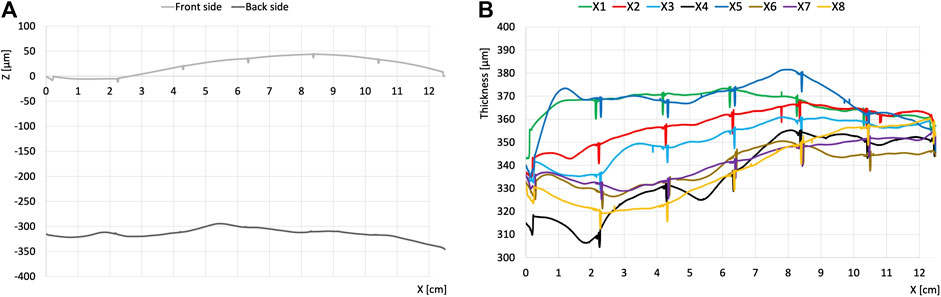
FIGURE 8. (A) front (gray) and back (black) profiles for WLP 6, X4: the distance between the two profiles is taken as the wafer thickness (B) distance extracted in the described procedure, for eight lines along the X axis of WLP 6. Combining the results, the average thickness of WLP 6 is 350 ± 16 μm.
Discussion of Results and Room for Improvements
WLP and FOWLP have been demonstrated a successful and mature technology for large scale integration and high miniaturization of multi-chip systems in commercial products. We made a first investigation on its usability in the field of pixel detectors for HEP applications. The initial test we conducted examines the possibility of using the instrumentation of a “standard” manufacturing line for typical silicon radiation sensor detectors.
Our test achieved some preliminary results, which we think we can improve, but are already good enough, or at least encouraging, to consider the WLP sensor for application in the new conceptual design of pixel detector modules. Main findings are:
1. achieved a minimum total WLP thickness of 350 µm using 300 µm dies. The produced WLPs are similar in brittleness to silicon wafers of the same thickness;
2. the inter-distances between the dies have a spread of 26 µm (standard deviation) in X and Y from nominal value. This spread is much larger than what was measured with glass scales to calibrate the flip-chip machine and we think that is mainly due to two factors: the flip-chip machine operating in imperfect conditions, due to the presence of bonding-film, distorts precise alignment and resin flow during compression which moves attached dies out of position on the wafer carrier. However, the value obtained is already good enough for the desired application and could be improved with the new flip-chip machine;
3. warpage of ∼500 µm for the thinnest WLP. Such value is significantly higher than that of a comparable size silicon wafer. We think we can improve with a mold made with harder material and with better mechanical precision than the one we made in aluminum. The space between the two chucks of the wafer bonding machine limits the total thickness of the mold and it undergoes deformation when the force of 15,000 N is applied;
4. chip bow in the thinnest WLP is of the order of one micron. This value is well compatible with bump-bonding process where the requirement for chip bow is ≤ 15 µm [14].
The obtained results provide encouraging achievement to the use of this technology for applications in a new generation of multi-chip pixel modules in the cases where the sensor tiles, for technology reason, are single chip tiles and cannot be used as support structure for multi-chip modules. This is what happens with 3D sensor or high-voltage CMOS detectors.
As case study of new conceptual design, we can consider the use of WLP associated with 3D sensors and compare the advantage of its use respect to the production flow used today. In present and future HEP experiments, the typical 3D pixel detector modules are assembled with 2, 3 (3 modules in-line) or 4 (2 × 2 quad-module) single chip modules. They are made as single modules connected together by gluing a flex-hybrid on top of them with a precision of the order of 50÷100 µm. The WLP similar modules would have a better mechanical precision, considering that already from our prototypes we have reached an accuracy of 25 µm.
Nowadays, 3D sensors are tested on wafers and good dies are selected before processing for bump deposition (in case of thermal compression indium bump process). Since the yield of 3D sensor is typically around 50%, the high cost of bump deposition is affected by the sensor yield. The use of WLPs made of only known good die sensors would decrease such cost also because 8-inch or larger WLP wafers could be used; instead, the typical production lines of 3D sensors are limited to 4-inch or 6-inch wafers.
3D sensor modules are made today by flip-chipping a front-end pixel read-out chip to a single-chip sensor tile. One of the bump-bonding processes uses thermo-compression of indium bumps deposited on both the detector and the front-end. This process is performed at relatively low temperatures (∼100 °C) and is compatible with the WLP resin having a Tg temperature of 170°C. Bumps could be deposited on the WLP wafer before singulation into modules.
For bump deposition, in the standard process, it is necessary to deposit a thick (15 µm) photoresist with openings on the metal pad of 12 µm typical. The process uses a glass mask covering the whole wafer.
In the case of the WLP we have to use a stepper photolithographic mask aligner that individually align the mask to every single sensor die. This apparatus is available in the production line we have used. It has a submicron precision and automatically aligns and exposes every chip stepping trough the reticule. Once photoresist is exposed, the process for bump deposition is the same as for normal wafers.
Once bumps are deposited, WLPs could be diced into modules of two, three or four front-end chip sizes and bump bonded as usual. Even if warpage is relatively large at level of wafer, the main concern for bump bonding is the warpage at the level of chip: a value of few micron is well compatible with the requirement of 10 µm bump height.
The introduction of WLP is already competitive at this level for performance and costs respect to standard process flow. However, the WLP process opens the world of post processing, which is largely addressed by industry, by adding FOWLP or the use of RDL on top of the WLP. In our case, for FOWLP we could use the stepper photolithographic mask aligner and precisely and automatically align and imprint electrical traces of bias voltages, power, ground and signals of read-out chip to simplify and optimize the interconnections before bringing out of the module. Today this is done on a flex hybrid circuit glued above the module. The WLP is an opportunity to rethink the module layout and optimize it for the wanted application.
Conclusions
We carried out preliminary tests, using typical tools available in a silicon foundry, to make WLPs with mechanical dummies of silicon sensors. The geometric measurements carried out on these WLPs have given encouraging results for the application of the technique in the field of monolithic and hybrid pixel detectors used in HEP experiments and pave the way for FOWLP and RDL in pixel module design.
Data Availability Statement
The raw data supporting the conclusions of this article will be made available by the authors, without undue reservation.
Author Contributions
PC, SG and FM designed and produced the silicon dummy wafer, put in place the WLP process at MicroFabSolution and produced the WLPs. The group in Genova (GD, AG, CG, AL and AV) was responsible for the measurements and data analysis mostly done by AL and AV. GD managed the project and access to funding. PC, GD and AL wrote the article.
Funding
This work was supported by the Italian National Institute for Nuclear Physics (INFN) with funding from National Commission I (RD_FASE2) and V (HVR_CCPD) and by the H2020 project AIDA-2020, GA no. 654168. The job position of AG, AL e AV were funded by the AIDA-2020 grant and INFN.
Conflict of Interest
The authors declare that the research was conducted in the absence of any commercial or financial relationships that could be construed as a potential conflict of interest.
Acknowledgments
The authors wish to thank G. Gariano and A. Rovani for the valuable and professional support given in the measurements made in the laboratory in Genova.
Footnotes
1MicroFabSolutions, Trento, Italy. https://www.microfabsolutions.com/wordpress
2Fondazione Bruno Kessler, Trento, Italy. https://www.fbk.eu/en
3ICROS™ from Mitsui Chemicals Tohcello, Inc. https://www.mc-tohcello.co.jp/icros/
4https://industrial.panasonic.com
References
1. Wermes N. Pixel detectors. where do we stand? Nucl Instrum Meth A (2019) 924:44. doi:10.1016/j.nima.2018.07.003
2. Parker SI, Kenney CJ, Segal J. 3D — A proposed new architecture for solid-state radiation detectors. Nucl Instrum Meth A (1997) 395:328. doi:10.1016/S0168-9002(97)00694-3
3. Da Via C, Boscardin M, Dalla Betta G‐F, Darbo G, Fleta C, Gemme C, et al. 3D silicon sensors: design, large area production and quality assurance for the ATLAS IBL pixel detector upgrade. Nucl Instrum Meth A (2012) 694:321. doi:10.1016/j.nima.2012.07.058
4. Peric I. Hybrid pixel particle-detector without bump interconnection. IEEE Trans Nucl Sci (2009) 56:519. doi:10.1109/TNS.2009.2014951
5. Snoeys W. Monolithic CMOS sensors for high energy physics. Nucl Instrum Meth A (2019) 924:51. doi:10.1016/j.nima.2018.06.034
6. Alimonti G, Andreazza A, Bulgheroni A, Corda G, Di Gioia S, Fiorello A, et al. Analysis of the production of ATLAS indium bonded pixel modules. Nucl Instrum Meth A (2006) 565:296. doi:10.1016/j.nima.2006.05.048
7. Alimonti G, Andreazza A, Corda G, Darbo G, Di Gioia S, Fiorello A, et al. Development of indium bump bonding for the ATLAS insertable B-layer (IBL). J Instrum (2013) 8:P01024. doi:10.1088/1748-0221/8/01/P01024
8. Lu JJ. (Invited) advances in materials and processes for 3D-TSV integration. ECS Trans (2012) 45:119–129. doi:10.1149/1.3700945
9. Lau JH. Recent advances and trends in fan-out wafer/panel-level packaging. J Electron Packag (2019) 141:040801–27. doi:10.1115/1.4043341
10. Wesling P. Heterogeneous integration roadmap: chapter 23 wafer level packaging (2019). Available online at: https://eps.ieee.org/images/files/HIR_2019/HIR1_ch23_WLP.pdf
11. Yeon S, Park J, Lee H-J. Compensation method for die shift caused by flow drag force in wafer-level molding process. Micromachines (2016) 7:95. doi:10.3390/mi7060095
12. Kumar A, Dingwei X, Sekhar VN, Lim S, Keng C, Sharma G, et al. Wafer level embedding technology for 3D wafer level embedded package. In 2009 59th electronic components and technology conference; 2009 May 26–29; San Diego, CA. San Diego, CA: IEEE (2009). p. 1289–96. doi:10.1109/ECTC.2009.5074177
Keywords: wafer level packaging, pixel detector, flip-chip, CMOS active pixel sensors, 3D pixel sensors, bump-bonding
Citation: Conci P, Darbo G, Gaudiello A, Gemme C, Girardi S, Lapertosa A, Mattedi F and Volpe A (2021) Wafer Level Packaging Technology Applied to Pixel Detectors. Front. Phys. 9:625685. doi: 10.3389/fphy.2021.625685
Received: 03 November 2020; Accepted: 14 January 2021;
Published: 25 February 2021.
Edited by:
Angela Kok, SINTEF DIGITAL, NorwayReviewed by:
Gabriele Giacomini, Brookhaven National Laboratory (DOE), United StatesStanislav Pospíšil, Institute of Experimental and Applied Physics, Czech Technical University in Prague, Czechia
Copyright © 2021 Conci, Darbo, Gaudiello, Gemme, Girardi, Lapertosa, Mattedi and Volpe. This is an open-access article distributed under the terms of the Creative Commons Attribution License (CC BY). The use, distribution or reproduction in other forums is permitted, provided the original author(s) and the copyright owner(s) are credited and that the original publication in this journal is cited, in accordance with accepted academic practice. No use, distribution or reproduction is permitted which does not comply with these terms.
*Correspondence: Giovanni Darbo, Z2lvdmFubmkuZGFyYm9AZ2UuaW5mbi5pdA==