 N. Demaria
- Istituto Nazionale di Fisica Nucleare (INFN), Sezione di Torino, Torino, Italy
The High Luminosity Large Hadron Collider (HL-LHC) at CERN will constitute a new frontier for the particle physics after the year 2027. Experiments will undertake a major upgrade in order to stand this challenge: the use of innovative sensors and electronics will have a main role in this. This paper describes the recent developments in 65 nm CMOS technology for readout ASIC chips in future High Energy Physics (HEP) experiments. These allow unprecedented performance in terms of speed, noise, power consumption and granularity of the tracking detectors.
1 Introduction
Microelectronics has always played a fundamental role in high energy particle physics research. Experiments are fundamentally based on specialized sensors producing an electrical signal upon incident ionizing particle. The signal needs to be amplified, shaped, time-stamped by the front-end electronics and eventually sent off-chip as analog or digital information for further processing (i.e., to boards hosting FPGAs). Information is then analyzed, first locally and then more globally using data from many sensors, or different parts of the apparatus to take decisions on the full event. The core performance of a detector is determined by the chosen sensor, the design and technology of the front-end electronics, together with their interconnection.
HEP experiments have to build more sophisticated detectors in order to exploit the new challenges that experimental particle physics needs to reach. Commercial microelectronics is in constant evolution with technology moving to more and more miniaturized circuits. Benefits are several in terms of logic integration, noise performance, speed, power consumption and low gate capacitance. Although these are major improvements for HEP, great care must be taken because front-end electronics requirements are very specific in scope. Electronics is normally custom-made due to the peculiar requirements of the sensors and of the data acquisition (DAQ) system of the experiment. Within the HEP community the responsibility for the electronics design is taken by a single institute or sometimes collaborations of several institutes are created, both during the R&D phase and the final design. Cost and accessibility are key elements to enable HEP research groups work on new technologies. Last but not least, radiation levels of many HEP experiment are largely above those typical in other fields, including space or military. For this reason, an extensive effort is required to well characterize the radiation resistance of every technology up to the level needed by the HEP experiments.
Figure 1A shows the evolution of industry through the years in developing new technologies and Figure 1B the number of papers published by the HEP community and relevant to R&D work focused on micro-electronics at different nodes. The number of papers does not illustrate the entire effort invested on R&D in a quantitative way but it does indicates on how and when these efforts evolved through time for the different technology nodes.
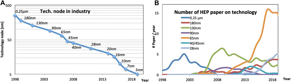
FIGURE 1. (A) development of technology nodes in industry (example from one factory); (B) Number of HEP papers relevant to R&D of microelectronics design where a specific CMOS technology is directly specified in the title: data shown are three years average and are obtained from a web based search tool.
Tracking detectors that measure the position of particle are the major drivers for the innovation of electronics in HEP. They are facing the extreme experimental challenges when accelerators are pushed to new physics regime, increasing energy or instant luminosity. Two are the main impacts of this. Firstly, particle density increases accordingly and therefore they need to scale down the dimension of the smallest sensitive area in order to maintain a good separation among particles and a high tracking efficiency. This implies they have to integrate more intelligence in the front-end electronics, while maintaining a low power budget, at least identical to the unit square area with respect to previous detectors in order to preserve the amount of material needed for cooling. Secondly, their electronics is required to survive to the radiation level that increases with integral luminosity. This level reaches its maximum in the inner layers of the experiment that are constituted by tracking detectors. The radiation resistance of MOS has the potential to improve with thinner gate dielectric and therefore might benefit from moving to a further miniaturization, at least for planar technologies.
In the year 2000 the main technology node was 0.25 μm, the so-called quarter micron technology. Its R&D in HEP was pushed primarily by the Large Hadron Collider (LHC) accelerator at CERN, where the first collisions started in 2009. The basic components of the detectors, modules composed of sensors and electronics, started to be built around 2004, and therefore technology choices were to be made at the latest on 2000, leading to the wide usage of quarter micron technology in the LHC. The boost of R&D on 0.25 μm started immediately, as it is visible in Figure 1, while the next innovation in HEP micro-electronics came with some delay with respect to its availability from industry. Only in 2006, a further step down to 130 nm CMOS node in HEP is visible and several detector upgrades of LHC detectors for the phase-1 upgrade were based on this technology.
The next boost has been determined by the HL-LHC program. The new HL-LHC accelerator will allow to reach a new frontier for the particle physics after 2027, as it will determine a factor of five to seven increase in instant luminosity at the LHC and a factor of ten integral luminosity.
The 65 nm CMOS technology node was chosen for detailed exploration for the need of HL-LHC experiments since, with respect to the130 nm CMOS node, allows for more compact digital logic and memories
Since the attractive solution of a monolithic detector cannot be pursued in the time due for the HL-LHC project, the basic solution for the inner layers of tracking detectors is based on a hybrid pixel detector approach. Also, monolithic detectors are limited in terms of speed for the sensitive part and of radiation hardness, at least in the case of the 130 nm or 110 nm processes that represent the nodes used at present for these detectors.
First studies on 65 nm CMOS technology in HEP began in 2010–2012, about three to four years after it was available from industry. Only in 2013, research has increased substantially in the community. A big boost was the formation of a specific R&D international collaboration, called RD531, and of a few projects as [1] or AIDA20202, all bringing together several experts to leverage this technology for HEP. This has allowed the achievement of considerable progress in several areas: understanding the radiation hardness of the technology; development of basic building blocks (DAC, ADC, Band-Gap, T-sensors, PLL, cable-driver, power-regulators, memory-cells, TDC, high-speed serializer); design of small, low power, fast analog front-ends; development of complex digital circuits; the application of Single Event Upset (SEU) mitigation techniques and their verification on real chips; the integration of large-size ASIC, with complex digital logic, I/O.
This paper describes the basic performance improvements and the new developments of ASIC for HEP that became possible (or will be in near future) thanks to the investment on 65 nm CMOS technology and major R&D work. An overview of applications and state-of-the-art for pixel detectors, tracking, timing detectors, high speed data links and others are presented. Table 1 shows the list of detectors implementing 65 nm CMOS technology for the HL-LHC experiments alongside with the main specifications and requirements.
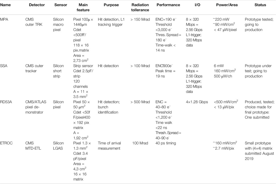
TABLE 1. Table showing main characteristics of HEP detectors developing micro-electronics in 65 nm. Data taken from paper listed in reference.
2 Radiation Hardness
In order to use new CMOS technology for HEP front-end electronics, a dedicated study of radiation effects is fundamental since the innermost regions of the experiment can reach unprecedented values of radiation level. In particular, the level of total ionizing dose (TID) in the tracking detectors can reach up to 0.5–1 Grad in the inner layers, values that are two-three orders of magnitude larger than in space applications. Immunity of critical digital circuits to Single Event Effects (SEE), in particular to SEU, are also important for a correct functioning of the electronics.
For the current LHC detectors, the 0.25 μW CMOS technology was characterized with TIDs of a few tens of Mrad, as expected for the innermost layers at the end of the LHC program, before entering to the HL-LHC. This led to the use of special enclosed MOS layout to avoid large leakage currents between source and drain [2], needing special digital cells. The 130 nm CMOS technology was proven to be more radiation hard, so that standard digital cell could be used up to almost 100 Mrad [3] without requiring special layouts techniques.
The first studies on 65 nm technology have shown [4, 5] that is more radiation hard than the previous nodes. Visible degradation begins at 100 Mrad and special precautions have to be taken if going up to 500 Mrad values, with most effects seen for small feature gates, in particular on p-MOS, rather than nMOS. The temperature during irradiation has an effect. More limited degradation is found at low temperature, than at room temperature [5, 6], as shown in Figure 2.
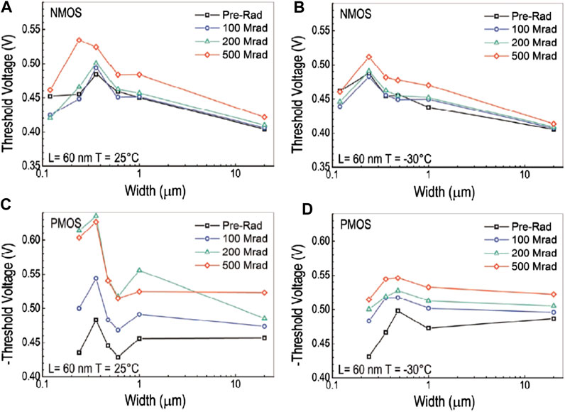
FIGURE 2. Threshold voltage vs. channel width in saturation mode for short nMOS (A,B) and pMOS (C,D) at room (A,C) and low (B,D) temperatures for different total dose irradiation From [6].
Analog circuits need to minimize performance variations, therefore they normally make use of large MOS gates to minimize mismatches. In general, small size MOS gates, that are suffering from larger degradation at high total dose, are avoided anyway in analog circuits. Nevertheless, a few design rules, vetoing small feature MOS, have been used to avoid weak points. The characterization of circuits before and after irradiation have shown good results, see Figure 3A.
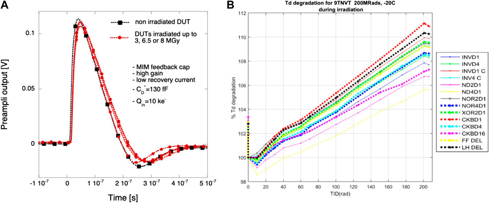
FIGURE 3. (A) Shape at different total dose irradiation for a preamplifier from a 50 x 50 μm2 pixel cell, from [24]; (B) Timing variation for different elements of 65 nm digital library from [25].
For a digital circuit, it is important to know the timing variations, both for combinational and sequential circuits, in order to make a detailed circuit verification that guarantees a good functioning in different corner situations. Measurements have been done on test structures with delay lines and ring oscillators, before and after irradiation, to quantify the effects for different components of the technology digital library. Results are shown in Figure 3B.
An extensive work have been done to characterize radiation effects on the technology, in order to introduce reliable models that allow designers to evaluate the effects on their circuits and to minimize them. Some works are found in Ref. [7], as shown in Figure 4.
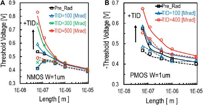
FIGURE 4. Threshold variation for nMOS (A) and pMOS(B) vs gate length: data points and model predictions, from [7].
3 Tracker Detectors
In the outer tracker, the CMS experiment has developed a solution that measures directly in the front-end the charged particle curvature, in order to use it as fundamental information for the L1-Trigger decision. A sandwich of a short silicon strip sensor and a pixel sensor is realized, each with its own front-end ASIC [8]. The pixel sensor is read out by a Macro Pixel ASIC (MPA) that receives the information from the strip sensor ASIC (SSA) simultaneously and has a logic that discriminates interesting particles with high transverse momentum. By using the pixel on one side, a good determination of the 3D direction is possible. Therefore, the MPA can provide particle momentum selection at 40 MHz for the L1-trigger. The schematics of the MPA-SSA is visible in Figure 5.
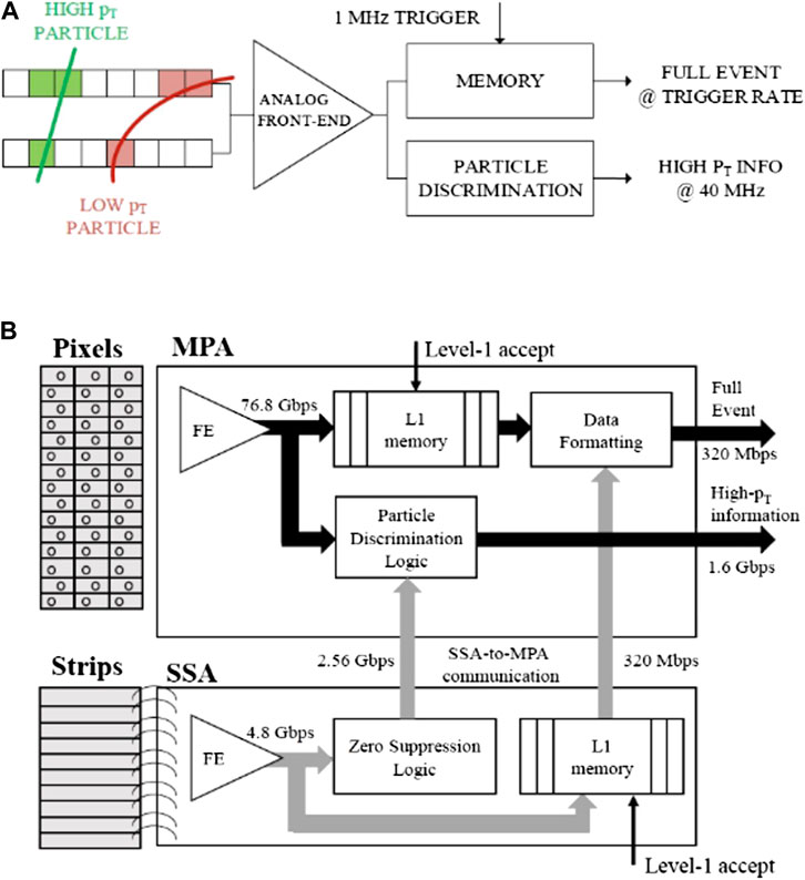
FIGURE 5. Schematic representation of the MPA-SSA concept, with two layers silicon sensor identifying an incident particle. Two hits identify a particle, the smaller the curvature of the trajectory, the largest the transverse momentum: this allows to quickly select high-pt L1 by correlating the position of the two hits (A). Schematics of digital logic are shown on (B) From [8].
For the MPA, the main challenges motivating the choice of 65 nm CMOS, are the limitation of the power-budget of the chip of 200–220 mW for a
The SSA [10, 11] needs to maintain low power consumption and to provide high radiation resistance. If it has already been discussed in Section 2 the benefit of using 65 nm CMOS for improved radiation hardness, in term of power it is interesting to compare the SSA with the CBC3 [12], the readout chip used in the silicon strip module at the larger radius of Outer Tracker and made in 130 nm CMOS technology. The power consumption of the SSA analog front-end is about 250 μW/ch while is about 330 μW/ch for the CBC3, therefore the gain here is marginal, and also due to the smaller capacitance of the silicon strip sensor. The real benefit of 65 nm CMOS is shown for the digital circuits. The SSA has eight 320 Mbps output lines, since the strip information have to be sent to MPA without zero-suppression, while the CBC3 provides less information outside the ASIC, with only one 40 Mbps data output. Despite the SSA has 64 times more data output than the CBC3, the digital power is only five times larger. The choice of 65 nm CMOS technology has been fundamental in order to accomplish a module with L1-trigger information obtained with a sandwich of a pixel sensor together with a strip sensor. The total power consumption of the SSA is about 500 μW/ch, for a total of 60 mW, to be compared to about 40 mW of the CBC3.
4 Vertex Detectors
A new pixel front-end chip, that guarantees high performance at HL-LHC for the inner tracking layers, must be developed for both the ATLAS and CMS detector upgrades. In this case the use of 65 nm CMOS is pushed to the maximum requirements. The pixel hit rate is up to 3 GHz/cm2, the granularity of the pixel must be increased by a factor of five with respect to previous state-of-the-art. The chip must work reliably with an efficiency above 99% when exposed to a harsh radiation environment with a total dose of up to 1 Grad. Meanwhile, low power consumption must also be maintained.
The requirements [13] for the final chip dimension is around 4 cm2, with a matrix of nearly 400x400 pixels and more logic in the chip periphery, determining a data readout of up to 3-4 Gbps. Fast output drivers, radiation hard and SEU resistant, must also be developed. Thin planar silicon sensors, with a thickness around 100–150 μm, are foreseen for a large fraction of the pixel detector, and this implies a smaller signal than for Phase-0 and Phase-1 detectors, with a most probable value (MPV) for an incident particle of around 6–7,000 e− after irradiation. This defines high requirements for the analog front-end, aiming very low threshold at a level below 1,200 e− and therefore a very low noise performance for the new chip.
For the pixel innermost layers, the CERN RD53 collaboration has gone through several steps, developing first analog and digital building blocks, all tested for irradiation, then designing and prototyping small scale demonstrators [14, 15] and eventually a large scale prototype, so called RD53A [16], that is 2 cm2 in size. Table 2 shows the evolution of these prototypes, with their different features. A high granularity, with a pixel dimension of 50 μm x 50 μm was successfully achieved, determining a big challenge for both analog and digital electronics of the matrix. Each shares 50% of area and power.
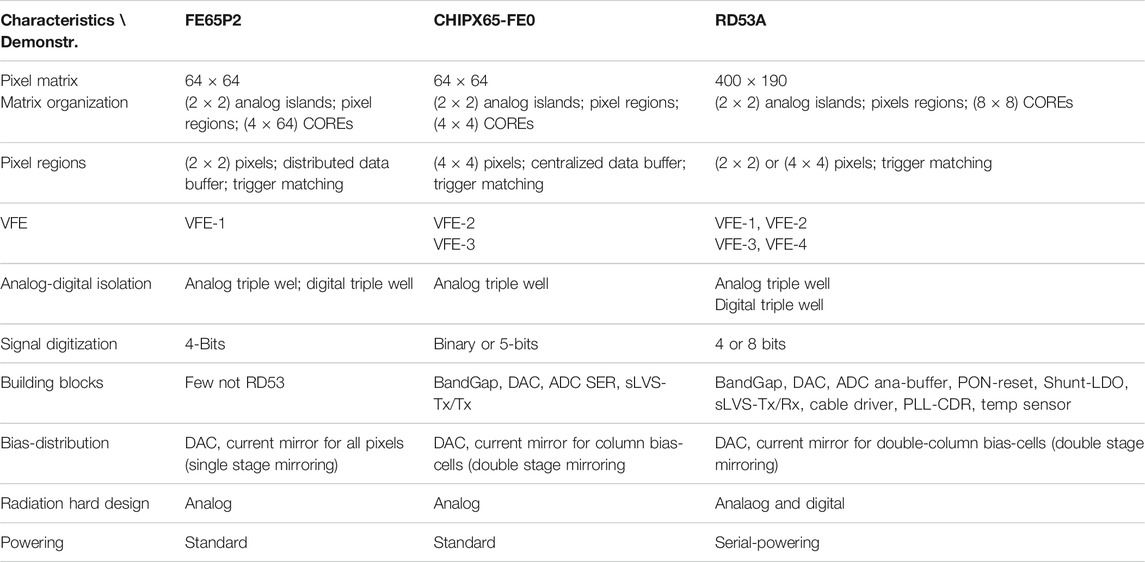
TABLE 2. Table with the different characteristics of FE65P2, CHIPIX-FE0, RD53A demonstrators, produced on Sept-2015, July-2016 and Aug-2017 respectively From [16].
Three analog front-end designs with different architectures have been realized [17]. All were proven to satisfy the requirements of RD53A, working at thresholds of about 1,200 e− with a noise occupancy at 10−6 level, a time-walk smaller than 25 ns and a charge deposition measurement with Time-of-Threshold (ToT) technique. Some results are shown in Figure 6. For ToT digitization four bit counting has been found to guarantee good spatial resolution and therefore has been preferred to higher values (5 or 6-bits) in order to determine small pile-up and to limit data readout.
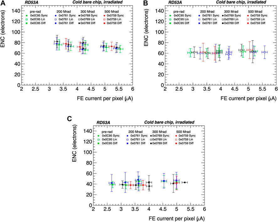
FIGURE 6. ENC vs current consumption for three different RD53A analog front-ends (A,B,C) at different irradiation doses From [26].
The digital matrix logic, has to handle the prospected high data rates for long L1-trigger latency (12.5 µs, more than double the value at LHC). It has been chosen to store locally the hit information within a region shared by several pixels. This architecture sends only the selected data to chip periphery, removing locally more than 98% of stored data. This results in a faster and low power data transfer to the chip periphery. Storing information from multiple hits of the same cluster translates to significant savings in storage resources; sharing of latency buffers by grouping pixels into so-called regions leads both to compact circuitry and low power. The exact way in which hit data are stored must be optimized for new requirements, taking into account the cluster size distribution, which in turn depends on the sensor type and the location in the detector, and on the physics input. Different solutions in RD53A have been evaluated with regions of
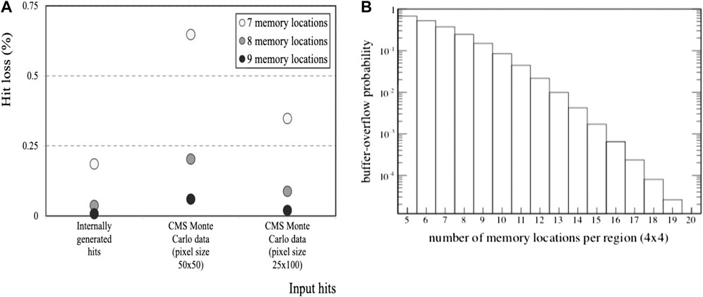
FIGURE 7. Hit losses determined by the dimension of the local pixel region data storage are shown for simulation studies in the case of
Measurements [20] of readout RD53A efficiency for different trigger latency vs single hit flux have been done. An X-ray source (60 kV Chrome target with a kα peak of 5.4 keV) generates a single hit physical signal to the silicon pixel sensor bump-bonded to RD53A. A calibration signal is injected to the pixel and, if not in pile-up with another hit, is eventually stored into a latency memory position that could eventually be overwritten by the continuous X-ray flux. The efficiency of getting the calibration signal measures the readout efficiency due to the limited memory storage and decreases with an increase of hit flux or trigger latency. Measurements results are shown in Figure 8: at 3 GHz/cm2 there is an overall efficiency of 99% and 97.5% for 3 and 12.5 μsec latency. Simulation predictions are also shown in Figure 8 and well agree with data for X-ray flux, validating the model used. In Figure 8 is also displayed the simulation results for charged particle, that presents clustered hits: a prediction of 1% inefficiency is obtained at 3 GHz/cm2 and 12.5 μsec latency, satisfying the requirements. The main cause of inefficiency is the four bit digitization of the very-front end signal, based on the Time-Over-Threshold technique, based on a 40 MHz clock for RD53A: with an average of roughly 8 counts, it implies a constraint in the analog dead-time of 200 ns that at the max flux rate of 3 GHz/cm2 implies 1% inefficiency. For the final design an equivalent 80 MHz digitization have been chosen to reduce this inefficiency by half.
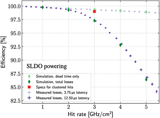
FIGURE 8. Efficiency vs hit rate flux generated by X-ray, that generate single hit clusters: data well fit the simulation prediction. Simulation prediction for clustered hits coming from particles are also shown, see text From [20].
The schematics of the RD53A periphery is shown in Figure 9 for the digital architecture and the connection to the I/O, sending data with four lines of 1.28 Gbit/s (pixel data and slow-control data) and receiving triggers and synchronous commands in a single differential line with 160 MHz clock. The need of a large bandwidth for data output, minimizing the amount of lines of readout, demands high frequency operation that can only be met by the 65 nm technology at these high radiation levels.
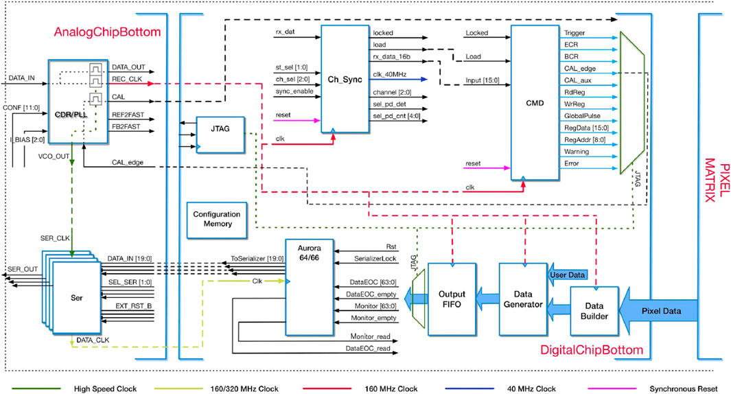
FIGURE 9. Schematics of digital RD53A periphery and connection to I/O From [16].
In terms of radiation hardness, RD53A was found to feature minor degradation at levels up to 500 Mrad for the digital circuitry and up to 800 Mrad for the analog.
The baseline prototype for CMS and ATLAS (called RD53B) is the evolution of RD53A, with improvements in many items, on the analog front-ends, digital architecture, I/O and the inclusion of several other features requested by the experiments, like data compression. A first version of RD53B has been submitted on March 2020 for the ATLAS experiment and is currently under test. A new version of the CMS pixel readout chip, again within the platform of RD53, is going to be submitted for production in the first quarter of 2021.
5 Timing Layers
The ETROC [21] is the readout ASIC in 65 nm technology foreseen as front-end for the Low Gain Avalanche Detector (LGAD) sensor pixel of the MIP Timing Detector (MTD) detector of CMS. The main design challenge is to extract precision timing information of 50 ps from the sensor with a capacitance of about 3.4 pF while keeping the power consumption low. The LGAD itself determines about 30 ps, while the system clock is designed to be precise at 15 ps, thus ETROC should perform at 40 ps The basic architecture is shown in Figure 10.
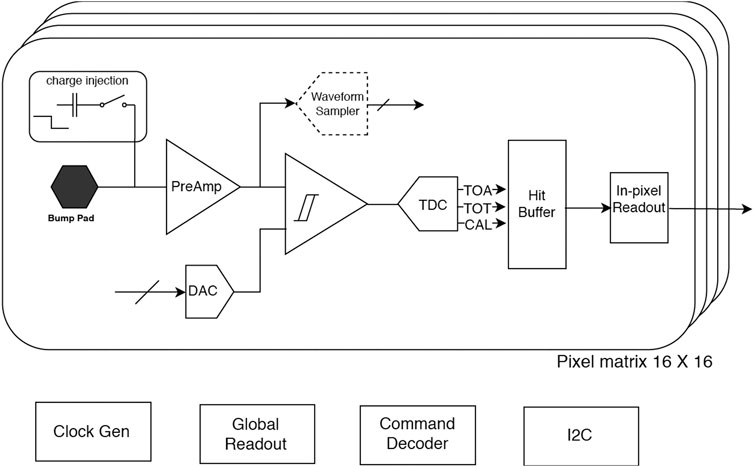
FIGURE 10. Schematics of ETROC From [21].
The small prototypes of the ETROC have been realized, with a single channel containing the preamplifier and discriminator (ETROC0) and a
6 High Speed Data Links
The upgraded detectors for HL-LHC have higher granularity, up to a factor of five or more with respect to present, while the L1 trigger rate foreseen from experiments will increase of an order of magnitude, from 100 kHz to almost 1 MHz. This implies an unprecedented data bandwidth to be read out by the front-end electronics. This has motivated the development of high speed links close to the detector for the necessary I/O, that should eventually guarantee sufficient radiation hardness and low power.
The low power GigaBit Transceiver (lpGBT) is a radiation tolerant ASIC that implements multipurpose high speed bidirectional links, with 2.56 Gb/s downlink and 5.12 or 10.24 Gb/s as uplink, providing Trigger, Data and Slow control information. It can receive several electrical up-links (E-links) from front-ends from 160 to 1,280 Mbps and send information with down-link with 80 to 320 Mbps. 3A schematics of the lpGBT is visible in Figure 11. A good reference can be found in [22] on the architecture and performance of the core part of this ASIC, as the PLL for data output and the CDR for the data input. The lpGBT is designed in 65 nm CMOS technology and represents the evolution of the GBT made in 130 nm. A comparison on the essential technical specifications of lpGBT and GBT is shown in Table 3 showing the considerable improvements made in high speed data links for HEP experiments with the use of 65 nm CMOS technology.
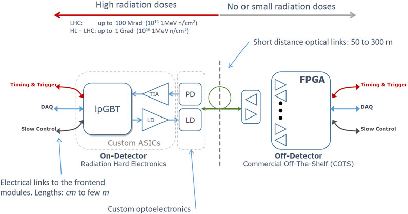
FIGURE 11. Schematics of lpGBT application From [22].
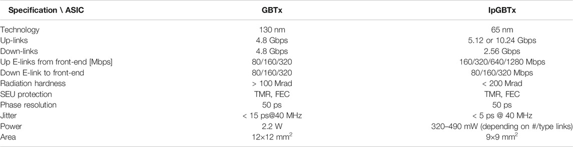
TABLE 3. Evolution of GBT to lpGBT, a comparison table of the essential specifications.
7 Conclusion
Progress in HEP experiments depends on innovation of detectors and the scaling of micro-electronics plays a fundamental role on that. To confirm this, this paper has shown how the use of 65 nm CMOS technology as a new tool for HEP has granted in many ways to reach new goals for the HL-LHC program. It allows integration of more local intelligence, to increase the detector granularity, or to achieve power reduction. It can improve the signals quality from the sensitive elements, as very low noise or fast timing. It can move larger amount of data or faster commands using high frequency clocks.
Future physics programs like ILC, CLIC, FCC will see the 65 nm CMOS as a baseline micro-electronics technology in several more detectors. Reduction in prices over time is normally expected for technologies, and this will make 65 nm CMOS even more attractive and accessible.
Other technology nodes are going to take the today role of 65 nm for HEP in the incoming years, and 28 nm CMOS is a good candidate. This node, as shown in Figure 1, is already being used in a few HEP R&D projects for small size ASIC. Moreover, radiation characterization [23] is quite advanced. CERN has recently launched a new R&D on experimental technologies. and 28 nm and FinFET CMOS technologies are among the key elements. This will make possible to establish in more solid grounds the access to the HEP for new innovative detectors.
Author Contributions
The author confirms being the sole contributor of this work and has approved it for publication.
Conflict of Interest
The author declares that the research was conducted in the absence of any commercial or financial relationships that could be construed as a potential conflict of interest.
Footnotes
1RD53 Collaboration web site: https://rd53.web.cern.ch/RD53.
2http://aida2020.web.cern.ch/aida2020/, WP4.
3https://ep-dep.web.cern.ch/rd-experimental-technologies.
References
1. Demaria N, Ciciriello F, Corsi F, Marzocca C, De Robertis G, Loddo F, et al. RD53 collaboration and CHIPIX65 project for the development of an innovative pixel front end chip for HL-LHC. Proc Sci (2015) IFD2014:010. doi:10.22323/1.219.0010
2. Anelli G, Campbell M, Delmastro M, Faccio F, Floria S, Giraldo A, et al. Radiation tolerant VLSI circuits in standard deep submicron CMOS technologies for the LHC experiments: practical design aspects. IEEE Trans Nucl Sci (1999) 46:1690–6. doi:10.1109/23.819140
3. Faccio F, Cervelli G. Radiation-induced edge effects in deep submicron CMOS transistors. IEEE Trans Nucl Sci (2005) 52:2413–20. doi:10.1109/TNS.2005.860698
4. Bonacini S, Valerio P, Avramidou R, Ballabriga R, Faccio F, Kloukinas K, et al. Characterization of a commercial 65 nm CMOS technology for SLHC applications. J Instrum (2012) 7:P01015. doi:10.1088/1748-0221/7/01/P01015
5. Menouni M, Barbero M, Bompard F, Bonacini S, Fougeron D, Gaglione R, et al. 1-Grad total dose evaluation of 65 nm CMOS technology for the HL-LHC upgrades. J Instrum (2015) 10:C05009. doi:10.1088/1748-0221/10/05/C05009
6. Chevas L, Nikolaou A, Bucher M, Makris N, Papadopoulou A, Zografos A, et al. Investigation of scaling and temperature effects in total ionizing dose (TID) experiments in 65 nm CMOS. In: 25th International conference on mixed design of integrated circuits and system (MIXDES); 2018 Jun 21–23; Gdynia, PolandIEEE. p. 313–8. doi:10.23919/MIXDES.2018.8436809
7. Nikolaou A, Bucher M, Makris N, Papadopoulou A, Chevas L, Borghello G, et al. Extending a 65nm CMOS process design kit for high total ionizing dose effects. In: 7th International conference on modern circuits and systems technologies (MOCAST); 2018 May 7–9; Thessaloniki, GreeceIEEE. p. 1–4. doi:10.1109/MOCAST.2018.8376561
8. Ceresa D, Kaplon J, Francisco R, Caratelli A, Kloukinas K, Marchioro A. A 65 nm pixel readout ASIC with quick transverse momentum discrimination capabilities for the CMS Tracker at HL-LHC. J Instrum (2016) 11:C01054. doi:10.1088/1748-0221/11/01/C01054
9. Ceresa D, Caratelli A, De Clercq J, Giovinazzo D, Kaplon J, Kloukinas K, et al. Characterization of the MPA prototype, a 65 nm pixel readout ASIC with on-chip quick transverse momentum discrimination capabilities. Proc Sci (2019) TWEPP2018:166. doi:10.22323/1.343.0166
10. Caratelli A, Ceresa D, Kaplon J, Kloukinas K, Leblebici Y, Murdzek J, et al. Short-strip ASIC (SSA): a 65nm silicon-strip readout ASIC for the pixel-strip (PS) module of the CMS outer tracker detector upgrade at HL-LHC. Proc Sci (2018) TWEPP2017:031. doi:10.22323/1.313.0031
11. Caratelli A, Scarfi S, Ceresa D, Kloukinas K, Kaplon J, De Clercq J, et al. Characterization of the first prototype of the silicon-strip readout ASIC (SSA) for the CMS Outer-Tracker phase-2 upgrade. Proc Sci (2019) TWEPP2018:159. doi:10.22323/1.343.0159
12. Raymond M, Braga D, Ferguson W, Fulcher J, Hall G, Jacob J, et al. The CMS binary chip for microstrip tracker readout at the SLHC. J Instrum (2012) 7:C01033. doi:10.1088/1748-0221/7/01/C01033
13. Chistiansen J, Garcia-Sciveres M. RD53 Collaboration proposal. Available from: https://cds.cern.ch/record/1553467 (Accessed February 19, 2021).
14. Garcia-Sciveres M, Carney R, Dunne K, Gnani D, Heim T, Hemperek T, et al. Results of FE65-P2 pixel readout test chip for high luminosity LHC upgrades. Proc Sci (2017) ICHEP2016:272. doi:10.22323/1.282.0272
15. Krueger E, Pacher L, Paternò A, Loddo F, Demaria N, Gaioni L, et al. A prototype of a new generation readout ASIC in 65nm CMOS for pixel detectors at HL-LHC. J Instrum (2016) 11:C12044. doi:10.1088/1748-0221/11/12/C12044
16. Demaria N, Barbero MB, Fougeron D, Gensolen F, Godiot S, Menouni M, et al. Recent progress of RD53 collaboration towards next generation pixel read-out chip for HL-LHC. J Instrum (2016) 11:C12058. doi:10.1088/1748-0221/11/12/C12058
17. Gaioni L, Manghisoni M, Re V, Riceputi E, Traversi G, Barbero MB, et al. RD53 analog front-end processors for the ATLAS and CMS experiments at the high-luminosity LHC. Proc Sci (2020) Vertex2019:21. doi:10.22323/1.373.0021
18. Conti E, Marconi S, Hemperek T, Christiansen J, Placidi P. Performance evaluation of digital pixel readout chip architecture operating at very high rate through a reusable UVM simulation framework. In: IEEE Nuclear Science Symposium, Medical Imaging Conference and Room-Temperature Semiconductor Detector Workshop (NSS/MIC/RTSD); 2016 Oct 29–Nov 6; Strasbourg, FranceIEEE. p. 1–4. doi:10.1109/NSSMIC.2016.8069646
19. Paternò A, Pacher L, Monteil E, Loddo F, Demaria N, Gaioni L, et al. A prototype of pixel readout ASIC in 65 nm CMOS technology for extreme hit rate detectors at HL-LHC. J Instrum (2017) 12:C02043. doi:10.1088/1748-0221/12/02/C02043
20. Ruini D. Serial powering and high hit rate efficiency measurement for the phase 2 upgrade of the CMS pixel detector. J Instrum (2019) 14:C10024. doi:10.1088/1748-0221/14/10/C10024
21.CMS. CMS MTD technical design report. Available from: https://cds.cern.ch/record/2667167 (Accessed February 19, 2021).
22. Biereigel S, Kulis S, Francisco R, Leitao P, LerouxMoreira PP, Prinzie J. The lpGBT PLL and CDR architecture, performance and SEE robustness. Pro Sci (2019) TWEPP2019:034. doi:10.22323/1.370.0034
23. Zhang C-M, Jazaeri F, Borghello G, Faccio F, Mattiazzo S, Baschirotto A, et al. Characterization and modeling of gigarad-TID-induced drain leakage current of 28-nm bulk MOSFETs. IEEE Trans Nucl Sci (2019) 66(1):38–47. doi:10.1109/TNS.2018.2878105
24. L. Ratti, L. Gaioni, M. Manghisoni, V. Re, E. Riceputi, G. Traversi. Charge preamplifier in a 65 nm CMOS technology for pixel readout in the Grad TID regime. In: 16th European Conference on Radiation and Its Effects on Components and Systems (RADECS); 2016 Sept 19–23; Bremen, GermanyIEEE. p. 1–5. doi:10.1109/RADECS.2016.8093110
25. Casas LMJ, Ceresa D, Kulis S, Miryala S, Christiansen J, Francisco R, et al. Characterization of radiation effects in 65 nm digital circuits with the DRAD digital radiation test chip. J Instrum (2017) 12:C02039. doi:10.1088/1748-0221/12/02/C02039
Keywords: CMOS, electronics, micro-electronic design, high energy physics experiments readout, high energy physics, pixel sensor circuit, sub micron, tracking detector
Citation: Demaria N (2021) The Impact of Microelectronics on High Energy Physics Innovation: The Role of 65 nm CMOS Technology on New Generation Particle Detectors. Front. Phys. 9:629028. doi: 10.3389/fphy.2021.629028
Received: 13 November 2020; Accepted: 14 January 2021;
Published: 08 March 2021.
Edited by:
Angela Kok, SINTEF DIGITAL, NorwayReviewed by:
Lodovico Ratti, University of Pavia, ItalyLeonello Servoli, Istituto Nazionale di Fisica Nucleare di Perugia, Italy
Copyright © 2021 Demaria. This is an open-access article distributed under the terms of the Creative Commons Attribution License (CC BY). The use, distribution or reproduction in other forums is permitted, provided the original author(s) and the copyright owner(s) are credited and that the original publication in this journal is cited, in accordance with accepted academic practice. No use, distribution or reproduction is permitted which does not comply with these terms.
*Correspondence: N. Demaria, ZGVtYXJpYUB0by5pbmZuLml0