 Xuehan Liu1
 Zhun Zhang
- 1Guangdong Provincial Key Laboratory of Nanophotonic Functional Materials and Devices, School of Information and Optoelectronic Science and Engineering, South China Normal University, Guangzhou, China
- 2Guangdong Women and Children Hospital, Guangzhou, China
A subwavelength metamaterial perfect absorber (MPA) in optical communication band was proposed and tested using the finite-difference time-domain method. The absorber is periodic and comprises a top layer of diamond silicon surrounded by L-shaped silicon and a gold layer on the substrate. It can achieve dual-band perfect absorption, and one of the peaks is in the optical communication band. By changing the gap (g) between two adjacent pieces of L-shaped silicon, and the thickness (h) of the silicon layer, the resonance wavelength of absorption peak can be tuned. When the incident electromagnetic wave entered the absorber, the metamaterial absorber could almost completely consume the incident electromagnetic waves, thereby achieving more than 99% perfect absorption. The absorption peak reaches 99.986% at 1310 nm and 99.421% at 1550 nm. Moreover, the MPA exposed to different ambient refraction indexes can be applied as plasma sensors, and can achieve multi-channel absorption with high figure of merit (FOM*) value and refractive index (RI) sensitivity. The FOM* values at 1310 nm and 1550 nm are 6615 and 168, respectively, and both resonance peaks have highly RI sensitivity. The results confirm that the MPA is a dual-band, polarization-independent, wide-angle absorber and insensitive to incident angle. Thence it can be applied in the fields of optical communication, used as a light-wave filter and plasma sensor, and so on.
1 Introduction
Electromagnetic metamaterials are an artificial composite structure or composite material with extraordinary electromagnetic properties that natural materials do not possess, and research on these materials has attracted considerable attention and made significant progress in recent years [1, 2]. Using electromagnetic metamaterials can achieve arbitrary “cutting” of electromagnetic and light wave properties, thus creating peculiar electromagnetic characteristics such as perfect lens [3, 4], negative refractive index [5], and electromagnetic stealth [6]. An attractive application field of metamaterials is the “perfect absorber” of electromagnetic waves [8, 9]. The concept of the perfect absorber was originally proposed by Landy et al in 2008 [10]. After then, a large range of absorbers with dielectric disks, ribbons, rings, and diamond arrays have been proposed and demonstrated [11–20]. In these studies, perfect absorbers in visible, infrared, and terahertz (THz) range were presented [21–28]. For instance, Li et al. proposed a novel broadband metamaterial perfect absorber based on visible light [12]. Xu et al. demonstrated an ultra-broadband metamaterial absorber in a frequency range of 3–7.8 THz [29]. A multi-channel plasmonic perfect absorber based on the mid-infrared region was proposed by Meng et al. [13]. A triple-band perfect absorber based on the infrared range was designed by Wu et al. [30]. Most of them are metamaterial-based electromagnetic resonance absorbers. By rationally designing the physical size and material parameters, the metamaterial can be coupled with the electromagnetic component of the incident electromagnetic wave, so that the electromagnetic waves incident on the specific broadband of the absorber can be 100% absorbed. At present, the potential applications of perfect absorbers include bolometer [10], electromagnetic stealth [31], and thermal emission [32].
Optical communication is a communication method using light waves as carriers. The two most obvious advantages of optical communications are transmission distance and capacity. Wavelength-division multiplexing technology ensures that the optical fiber system has a strong transmission capacity, so it can be applied to cross-sea communication systems. Optical communication also has an extremely wide transmission frequency band, with high information-transmission efficiency and a strong ability to resist electromagnetic interference, which can maintain high communication-transmission quality in various application environments. Furthermore, the optical communication bands have the lowest loss, the smallest dispersion, and the lowest microbending loss, providing a comprehensive array of applications in optical amplifier long-distance trunk systems and submarine cable systems. Therefore, we planned to combine the metamaterial perfect absorber with the optical communication band for our study, that is, we want to realize the resonance absorption window in the optical communication band.
In this article, a metamaterial perfect absorber (MPA) in optical communication band is proposed. The absorber comprises a diamond silicon surrounded by four L-shaped pieces of silicon, which were placed on a metallic plate to prevent energy from seeping out of the system. The number of electromagnetic response modes of the top structural unit determines the number of metamaterial absorption peaks; therefore, our proposed absorber has dual-band perfect absorption. Finite-difference time-domain (FDTD) simulations showed that there are two absorption peaks above 99% after optimization, and the wavelength of one of the absorption peaks was at an optical communication wavelength. According to the effective medium theory [7], the characteristics of metamaterials can be characterized by the effective dielectric constant and permeability, whereas the effective dielectric constant and permeability of metamaterials can be controlled by the orderly design of the material's key physical dimensions. Therefore, the resonance wavelength of absorption peak can be tuned by changing the geometrical dimensions of the structure, such as gap (g) between two adjacent L-shaped pieces of silicon, and the thickness (h) of the silicon layer. In addition, the designed MPA achieves near-perfect polarization independence and incident angle-insensitive dual-band light absorption. For the incident angle, the simulation results show that the designed structure realizes wide-angle absorption of 0°–40° for TM waves and TE waves, displaying a relatively perfect absorption effect. Moreover, the MPA exposed to different ambient refraction indexes can be applied to the field of plasma sensors, and can achieve multi-channel absorption with high FOM* value and RI sensitivity. The proposed subwavelength structure has important value in the fields of light-wave filters, thermal radiation meters, array thermal imaging detectors, and electromagnetic wave modulators.
2 Materials and Methods
The structure stereogram of the proposed MPA is shown in Figure 1A. There are four L-shaped [33–36] structures of the same size in a unit cell, as shown in Figure 1B. The upper layer is a resonator formed by a structure in which four L-shaped dielectrics surround a diamond-shaped dielectric, and the lower layer is a metal substrate. The optimized parameters of each part of 1310 nm structure and 1550 nm structure are marked in Table 1. Here, the resonance wavelength of the absorption peak was tuned by changing the structural parameters of the absorber to move the absorption peak from 1310 nm to 1550 nm. The two arm lengths of L-shaped silicon, distance between each two adjacent L-shaped silicon, thickness of the patterned silicon layer and structural periodicity are fixed at L, g, h and P, respectively. The arm widths of L-shaped silicon, semi-major axis and semi-minor axis of the diamond silicon are W, a and b, respectively. In the simulations, the incident light appears perpendicularly on the patterned silicon structure metamaterial absorber in the negative direction of the z-axis, with the electric field along the x direction and the magnetic field along the y direction. The mesh size in a patterned silicon layer is ∆x = ∆y = 4 nm, and ∆z = 6 nm. The simulation time and mesh accuracy were set to 15,000 (fs) and 4, respectively. The permittivity of Si and Au in the near-infrared region were obtained from the experiments of Palik and CRC [41]. The periodic boundary conditions were set in both x and y directions to reproduce this array, and the boundary condition along the z direction was the perfectly matched layer (PML) to eliminate scattering.
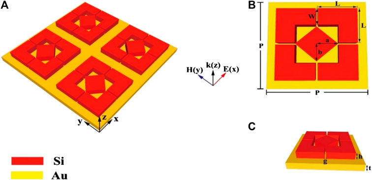
FIGURE 1. (A) Perspective view of the MPA device structure. (B) Top view of the unit cell structure. (C) Side view of the unit cell structure.
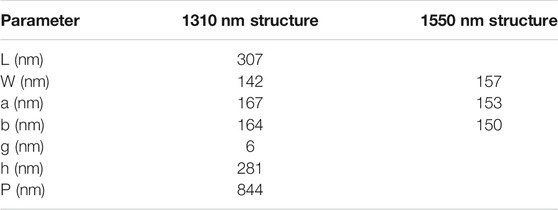
TABLE 1. Comparison of parameters of 1310 nm structure and 1550 nm structure.
The material of the metal substrate is gold, and the thickness of the gold reflection mirror is defined as t = 100 nm. The skin depth δ (or penetration depth) commonly used in engineering to characterize the skin depth of electromagnetic waves, which is defined as the distance the electromagnetic wave travels when the amplitude of the electromagnetic wave is attenuated to the surface value
therefore,
where ω is the angular frequency of the electromagnetic wave, μ is the magnetic permeability, and σ is the electrical conductivity. The thickness of the bottom metal plate is calculated as 100 nm, which is much greater than the skin depth δ of gold in this wavelength range. Therefore, the electromagnetic wave cannot penetrate the metal layer, the transmission coefficient of the absorber structure is always 0, and the absorption is only affected by the reflection coefficient. When electromagnetic waves occur on the metamaterial structure, electric field resonance and magnetic field resonance will occur in the absorber, accompanied by the generation of effective dielectric constant
where
which equals zero, and where
which is almost equal to zero. The electromagnetic wave is confined to the inside of the structure until it is completely consumed by the dielectric layer or the metal layer. According to Kirchhoff's theorem, the sum of absorptance A, transmittance T, and reflectance R is equal to 1, that is, A+ T + R = 1, so the absorptance is
It can be seen from Eq. 7 that if the frequency corresponding to the incident spatial impedance of the electromagnetic wave and the impedance of the dielectric layer have Z = Z0, the electromagnetic wave is absorbed without reflection, and the electromagnetic wave of a specific wavelength band can be absorbed at close to 100%.
3 Results and Discussion
Tunable Hybrid Metamaterial Absorber
The absorption spectrum of the proposed MPA in the optical communication band as a function of wavelength was calculated, as seen in Figure 2. The black solid line indicates that the peak on the left (labeled M) in the absorption spectrum corresponds to a wavelength of 1310 nm, and the peak value at M is up to 99.986%, so we call it 1310 nm for short. The red solid line indicates that the peak on the right (labeled N) in the absorption spectrum corresponds to a wavelength of 1550 nm, and the absorption at N reaches 99.421%; thus, we simply call it 1550 nm. Through a comparison of Table 1, we found that the resonant wavelength could be effectively tuned from 1310nm to 1550 nm by changing the semi-major axis (a) and the semi-minor axis (b) of the diamond silicon, and the arm widths (W) of the L-shaped silicon. The spectrum is shown in Figure 2.
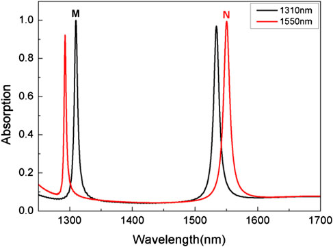
FIGURE 2. Simulated absorbance of the proposed MPA, whose structure is shown in Figure 1. The black solid line and the red solid line correspond to wavelengths of 1310 nm and 1550 nm, respectively. The corresponding peak at 1310 nm is labeled M, and the corresponding peak at 1550 nm is labeled N.
To better understand the physical mechanism of the proposed dual-channel perfect absorption, the electric and magnetic field intensity distributions of the unit cell structure at M and N are shown in Figure 3. The top (xoy) planes and cross-sectional (xyz) planes are plotted. In Figure 3A, it can be seen that the electric field at 1310 nm is mainly distributed between the closely adjacent diamond silicon and L-shaped silicon due to the localized surface plasmon resonance (LSPR), whereas the strong magnetic field is distributed in the diamond. This indicates that there is both electric dipole resonance and magnetic dipole resonance at the 1310 nm wavelength [15, 42, 43]. However, contrary to the electromagnetic field intensity distribution at 1310 nm, it can be clearly seen from Figure 3B that at the 1550 nm wavelength, the enhanced electric field is mainly concentrated between the bottom of the resonator and the gold film of the reflective layer. There is also a partly weak electric field distribution between the resonators, and the magnetic field strength is distributed in the dielectric layer. The reason is that a strong enhancement of the localized electromagnetic field is excited at the resonance frequencies between the two layers, and this effect results in almost zero reflectance observed in simulations and calculations [16]. These characteristics confirm that the absorption at the 1550 nm wavelength is caused by the coupling of the dipole resonance of the resonator and the second resonance of the silicon wafer.
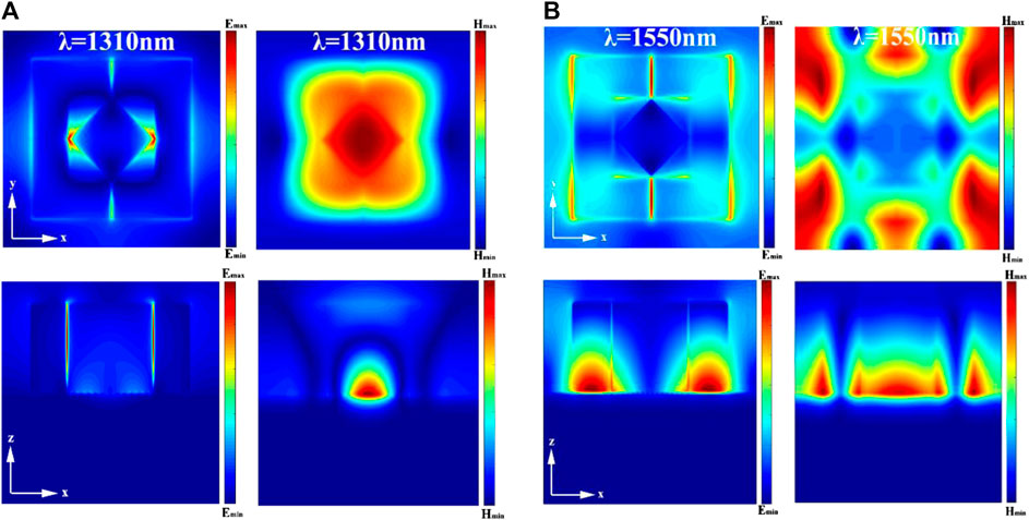
FIGURE 3. Electric and magnetic field intensity distribution diagram of the top planes (xoy) and cross-sectional planes (xyz) of the unit cell structure at the absorption peak of (A) 1310 nm, and (B) 1550 nm.
To further understand the working mechanism of the proposed MPA, the absorption under different structural parameters was studied. Figure 4 shows the calculated absorption intensity for the structure at 1310 nm and 1550 nm by varying the g parameter. For these two wavelengths, both the g values were changed from 2 nm to 18 nm, with an interval of 4 nm. The trends of both wavelengths with the change of g value are almost the same, as shown in Figures 4A,B. The absorption peaks of both wavelengths are blue-shifted with the increases of g value. The plasmon resonance will occur when SPPs resonate on the horizontal surface of L-shaped silicon, and the resonance conditions of L-shaped silicon can be expressed as [30].
where ksp = 2πnsp/λm, nsp is the effective index of SPPs and λm is the resonance wavelength, and Leqv denotes the equal resonance arm length, δ means the phase change at the end of the horizontal arms, and
It can be discovered from Formula (9) that the resonance wavelength is proportional to the effective arm length of the L-shaped silicon, and the absorption peak undergoes a redshift as the arm length (L) increases. However, the sum of L and g is fixed: as g increases, L decreases, which is presented in Figure 4.
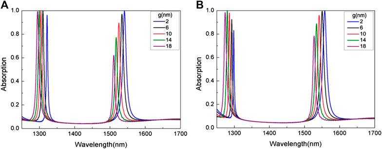
FIGURE 4. Absorption spectrum for different gaps (g) between two adjacent L-shaped silicon of (A) 1310 nm and (B) 1550 nm. Other parameters are consistent with those in Figure 1.
The next observation is the effect of different thicknesses of the silicon layer on the absorption spectrum, and the results obtained are shown in Figure 5. Other geometric parameters remain unchanged, and the thickness (h) of the silicon layer increases from 261 nm to 301 nm, with an interval of 10 nm. It can be seen from Figures 5A,B that both absorption peaks experience a redshift with the increase of h.
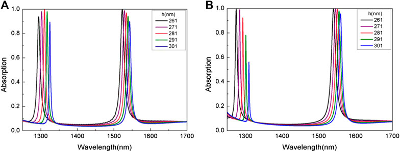
FIGURE 5. Absorption spectrum for the silicon layer h with different thicknesses at (A) 1310 nm and (B) 1550 nm. Other structural parameters are consistent with those in Figure 1.
Polarization independence and incident angle insensitivity are important factors that should be considered in practical applications. Figure 6 and Figure 7 show the influence of the incident angle in the TM mode and TE mode and the polarization angle on the absorption performance in the 1310 nm and 1550 nm structures, respectively. It can be seen that as the incident angle increases from 0° to 40°, the absorption peak still achieves nearly uniform perfect absorptance at the resonance frequency. It indicates that the absorption of the absorber is insensitive to the incident angle, the reason may be due to the structural symmetry of the absorber. Figure 6C and Figure 7C show the relationship between the variety of polarization angle and the absorption spectrum under normal incidence. Due to the high symmetry and the local resonance of the structure, the position and intensity of the absorption peak remain almost unchanged when the polarization angle changes from 0° to 90° in 10° increments at normal incidence. Therefore, the metamaterial absorber is independent of polarization. Polarization-insensitive metamaterial perfect absorbers have been widely used in optoelectronic devices including thermoelectric devices.
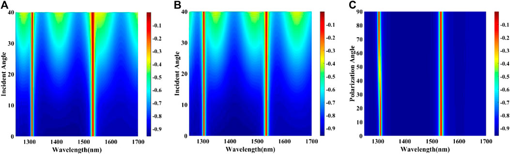
FIGURE 6. In the 1310 nm structure, tuned incident angle from 0° to 40° in (A) TM mode and (B) TE mode, and (C) the variety of polarization angle from 0° to 90° under normal incidence.
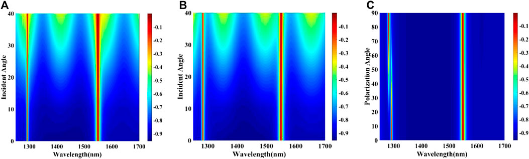
FIGURE 7. In the 1550 nm structure, tuned incident angle from 0° to 40° in (A) TM mode and (B) TE mode, and (C) the variety of polarization angle from 0° to 90° under normal incidence.
Tunable Hybrid Metamaterial Sensor
The reflectance spectrum with different ambient refractive indices at 1310 nm and 1550 nm are illustrated in Figure 8A and Figure 9A, respectively. They are both red-shifted by increasing the refraction index from 1.334 to 1.364, and the reflection intensities is decreasing. Here, we take the high-frequency reflection wavelength (near 1400 nm) in Figure 8A and Figure 9A as an example to obtain the relationship between resonance wavelength and refractive index, as shown in Figure 8B and Figure 9B. The black dots are the resonant wavelengths under different ambient refraction indexes, the red line is obtained by linear fitting, and the fitting degree is close to or equal to 1. And these two images have a common point that the resonance wavelength increases with the increase of refractive index. Moreover, the low-frequency and high-frequency RI sensitivities of the 1310 nm structure are 185.1 nm/RIU, 300.0 nm/RIU, respectively. The low-frequency and high-frequency RI sensitivities of the 1550 nm structure are 168 nm/RIU and 328 nm/RIU, respectively. The results show that the two resonance peaks of the absorber both have high sensitivity and can be used in the field of dual-band sensors.
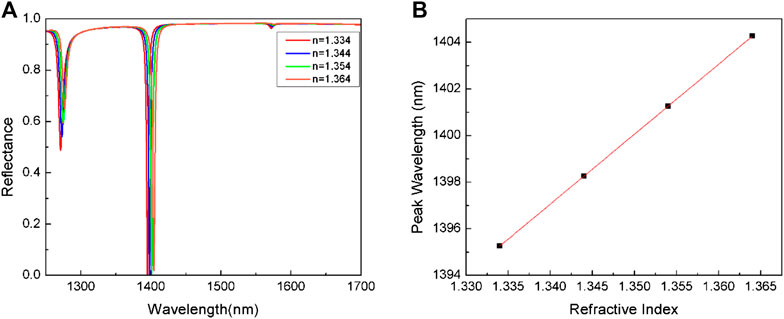
FIGURE 8. (A) The reflectance spectra exposed to different ambient refraction indexes, and (B) the relationship between resonance wavelength and refractive index in 1310 nm structure.
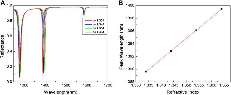
FIGURE 9. (A) The reflectance spectra exposed to different ambient refraction indexes, and (B) the relationship between resonance wavelength and refractive index in 1550 nm structure.
We used figure of merit (FOM*) to measure the sensitivity of the refractive index sensor. The FOM* value means the change in reflectance intensity caused by the diversification in the ambient refractive indices around the perfect absorber. The larger the FOM* value, the higher the sensitivity of the refractive index sensor. The expression is as follows [44]:
where
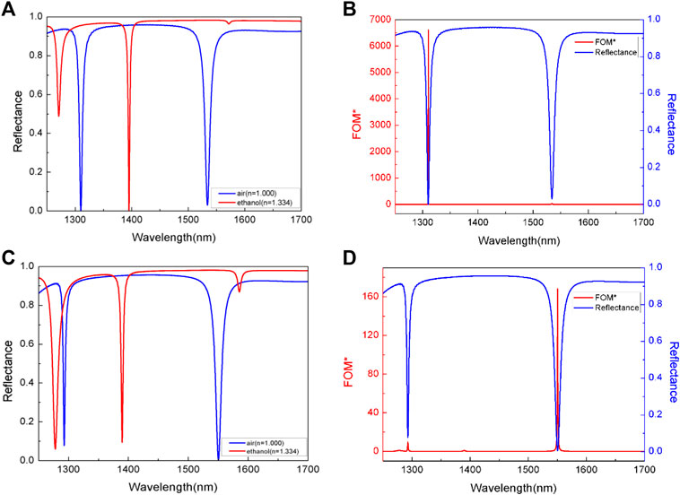
FIGURE 10. (A,C) Reflectance spectra and (B,D) FOM* values of 1310 nm and 1550 nm structures with air and ethanol solution as medium.
The system that plasma sensor for detection of chemical solution concentration is shown in Figure 11. The light source firstly weakens the light intensity through optical attenuator, and then enters the plasma sensor by transmission fiber and coupler. The light being modulated by the detection sample in the sensing area is received by the spectrometer, and it performs photoelectric conversion in the spectrometer and records the signal processing unit in real time. Finally, the detection signal can be obtained by normalized spectral processing.
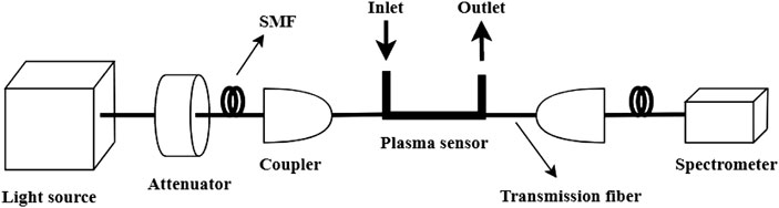
FIGURE 11. Diagram of system device used for chemical solution concentration detection.
4 Conclusion
A metal-dielectric dual-channel metamaterial perfect absorber in the optical communication band was proposed, and a single patterned silicon layer and a bottom gold layer were used for structural design. The simulation of the designed subwavelength structure was carried out using the FDTD method. By designing and optimizing the structure, size, and arrangement of metamaterial artificial units, the effective dielectric constant of the absorbing material is equal to the effective magnetic permeability, the electromagnetic wave of this frequency band completely enters the absorber and is hardly reflected, which will cause perfect absorption of the incident wave, thereby achieving a high absorption rate. The regulation of the resonance absorption position with the structural parameters was studied further. The effective adjustment of the absorption peak position was achieved by changing the arm length, thickness of the dielectric layer. Moreover, the combination of four identical L-shaped and diamond-shaped structures could achieve dual-band perfect absorption, and was polarization independent, wide-angle, incident-angle insensitive. The absorber can be used as a refraction index sensor. The results show that the FOM* values at 1310 nm and 1550 nm are the highest, at 6615 and 168, respectively. The calculated high RI sensitivity further showed that the designed perfect absorber could be used in the field of detectors, sensors and filters, with the potential for application in related fields.
Data Availability Statement
The original contributions presented in the study are included in the article/Supplementary Material, further inquiries can be directed to the corresponding author.
Author Contributions
Conceptualization, ZW and ZZ; methodology, ZZ; software, XL; validation, XL, ZW, KL, and ZZ; formal analysis, ZW and ZZ; investigation, XL; resources, XL, KL, ZM; data curation, XL, ZM, and KL; writing—original draft preparation, XL; writing—review and editing, XL and ZW; visualization, ZW; supervision, ZZ; project administration, ZZ; funding acquisition, ZW. All authors have read and agreed to the published version of the manuscript.
Funding
This work was supported by the National Natural Science Foundation of China (NSFC) under Grant No. 61774062.
Conflict of Interest
The authors declare that the research was conducted in the absence of any commercial or financial relationships that could be construed as a potential conflict of interest.
Acknowledgments
The Science and Technology Program of Guangzhou (No. 2019050001).
References
1. Sreekanth KV, ElKabbash M, Caligiuri V, Singh R, De Luca A, Strangi G. Graphene and topological insulator-based active THz hyperbolic metamaterials. In New Directions in thin film nanophotonics, progress in optical science and Photonics. Singapore: Springer (2019) 6:159–72. doi:10.1007/978-981-13-8891-0_9
2. Chang YC, Kildishev AV, Narimanov EE, Norris TB. Metasurface perfect absorber based on guided resonance of a photonic hypercrystal. Phys Rev B (2016) 94:155430. doi:10.1103/PhysRevB.94.155430
3. Pendry JB. Negative refraction makes a perfect lens. Phys Rev Lett (2000) 85:3966–9. doi:10.1103/PhysRevLett.85.3966
4. Casse BDF, Lu WT, Huang YJ, Gultepe E, Menon L, Sridhar S. Super-resolution imaging using a three-dimensional metamaterials nanolens. Appl Phys Lett (2010). 96: 1–3. doi:10.1063/1.3291677
5. Ramakrishna SA, Grzegorczyk TM. Physics and applications of negative refractive index materials. Bellingham, Washington: CRC (2008) 1–415. doi:10.1201/9781420068764
6. Liu R, Ji C, Mock JJ, Chin JY, Cui TJ, Smith DR. Broadband ground-plane cloak. Science (2009). 323:366–9. doi:10.1126/science.1166949
7. Smith DR, Pendry JB. Homogenization of metamaterials by field-averaging. J Opt Soc Am B (2006) 23:391–403. doi:10.1364/JOSAB.23.000391
8. Wang Z, Tong Z, Ye Q, Hu H, Nie X, Yan C, et al. Dynamic tuning of optical absorbers for accelerated solar-thermal energy storage. Nat Commun (2017) 8:1478. doi:10.1038/s41467-017-01618-w
9. Monti A, Alù A, Toscano A, Bilotti F. The design of optical circuit-analog absorbers through alectrically small nanoparticles. Photonics (2019) 6:26. doi:10.3390/photonics6010026
10. Landy NI, Sajuyigbe S, Mock JJ, Smith DR, Padilla WJ. Perfect metamaterial absorber. Phys Rev Lett (2008) 100:207402. doi:10.1103/PhysRevLett.100.207402
11. Zhao X, Wang Y, Schalch J, Duan G, Cremin K, Zhang J, et al. Optically modulated ultra-broadband all-silicon metamaterial terahertz absorbers. Acs Photon (2019) 6:830–7. doi:10.1021/acsphotonics.8b01644
12. Li C, Fan H, Wei Z, Lan S, Liu H. Multipole resonance in arrays of diamond dielectric: a metamaterial perfect absorber in the visible regime. Nanomaterials (2019) 9:1222. doi:10.3390/nano9091222
13. Meng HY, Xue XX, Lin Q, Liu GD, Zhai X, Wang LL. Tunable and multi-channel perfect absorber based on graphene at mid-infrared region. Appl Phys Express (2018) 11:052002. doi:10.7567/APEX.11.052002
14. Pradhan JK, Anantha Ramakrishna S, Rajeswaran B, Umarji AM, Achanta VG, Agarwal AK, et al. High contrast switchability of VO2 based metamaterial absorbers with ITO ground plane. Opt Express (2017) 25:9116–21. doi:10.1364/OE.25.009116
15. Lu X, Wan R, Zhang T. Metal-dielectric-metal based narrow band absorber for sensing applications. Opt Express (2015) 23:29842–7. doi:10.1364/oe.23.029842
16. Zhang B, Zhao Y, Hao Q, Kiraly B, Khoo IC, Chen S, et al. Polarization-independent dual-band infrared perfect absorber based on a metal-dielectric-metal elliptical nanodisk array. Opt Express (2011) 19:15221–8. doi:10.1364/OE.19.015221
17. Ke S, Wang B, Huang H, Long H, Wang K, Lu P. Plasmonic absorption enhancement in periodic cross-shaped graphene arrays. Opt Express (2015) 23:8888–900. doi:10.1364/OE.23.008888
18. Si J, Dong Z, Yu X, Deng X. Tunable polarization-independent dual-band coherent perfect absorber based on metal-graphene nanoring structure. Opt Express (2018) 26:21768–77. doi:10.1364/OE.26.021768
19. Ra’di Y, Asadchy VS, Kosulnikov SU, Omelyanovich MM, Morits D, Osipov AV, et al. Full light absorption in single arrays of spherical nanoparticles. ACS Photon (2015) 2:653–60. doi:10.1021/acsphotonics.5b00073
20. Alessio M, Andrea A, Alessandro T, Filiberto B. Narrowband transparent absorbers based on ellipsoidal nanoparticles. Appl Opt (2017) 56:7533–8. doi:10.1364/AO.56.007533
21. Yao G, Ling F, Yue J, Luo C, Ji J, Yao J. Dual-band tunable perfect metamaterial absorber in the THz range. Opt Express (2016) 24:1518–27. doi:10.1364/OE.24.001518
22. Sun P, You C, Mahigir A, Liu T, Xia F, Kong W, et al. Graphene-based dual-band independently tunable infrared absorber. Nanoscale (2018) 10:15564–70. doi:10.1039/c8nr02525h
23. Fann CH, Zhang J, ElKabbash M, Donaldson WR, Michael Campbell E, Guo C. Broadband infrared plasmonic metamaterial absorber with multipronged absorption mechanisms. Opt Express (2019) 27:27917–26. doi:10.1364/OE.27.027917
24. Xu H, Hu L, Lu Y, Xu J, Chen Y. Dual-band metamaterial absorbers in the visible and near-infrared regions. J Phys Chem C (2019) 123:10028–33. doi:10.1021/acs.jpcc.9b00434
25. De Souza ILG, Rodriguezesquerre VF. Design of planar and wideangle resonant color absorbers for applications in the visible spectrum. Sci Rep (2019) 9, 7045. doi:10.1038/s41598-019-43539-2
26. Peng C, Ou K, Li G, Li X, Wang W, Zhao Z, et al. Tunable phase change polaritonic perfect absorber in the mid-infrared region. Opt Express (2020) 28:11721–9. doi:10.1364/OE.390000
27. Wu P, Zhang C, Tang Y, Liu B, Lv L. A perfect absorber based on similar fabry-pert four-band in the visible range. Nanomaterials (2020) 10:488. doi:10.3390/nano10030488
28. Rana AS, Mehmood MQ, Jeong H, Kim I, Rho J. Tungsten-based ultrathin absorber for visible regime. Sci Rep (2018) 8:2443. doi:10.1038/s41598-018-20748-9
29. Xu Z, Wu D, Liu Y, Liu C, Yu Z, Yu L, et al. Design of a tunable ultra-broadband terahertz absorber based on multiple layers of graphene ribbons. Nanoscale Res Lett (2018) 13:143. doi:10.1186/s11671-018-2552-z
30. Wu D, Wang M, Feng H, Xu Z, Liu Y, Xia F, et al. Independently tunable perfect absorber based on the plasmonic properties in double-layer graphene. Carbon (2019) 155:618–23. doi:10.1016/j.carbon.2019.09.024
31. Schurig D, Mock JJ, Justice BJ, Cummer SA, Pendry JB, Starr AF, et al. Metamaterial electromagnetic cloak at microwave frequencies. science (2006) 314:977–80. doi:10.1126/science.1133628
32. Watts CM, Liu X, Padilla WJ. Metamaterial electromagnetic wave absorbers. Adv Mater Weinheim (2012) 24:OP98-120. doi:10.1002/adma.201200674
33. Xiang Y, Wang L, Lin Q, Xia S, Qin M, Xiang Z. Tunable dual-band perfect absorber based on L-shaped graphene resonator. IEEE Photonic Tech L (2019) 31:483–6. doi:10.1109/LPT.2019.2900269
34. Bai Y, Zhao L, Ju D, Jiang Y, Liu L. Wide-angle, polarization-independent and dual-band infrared perfect absorber based on L-shaped metamaterial. Opt Express (2015) 23:8670–80. doi:10.1364/OE.23.008670
35. Wang A, Qu S, Yan M, Wang W, Wang J, Zheng L, et al. Six-band polarization-insensitive perfect metamaterial absorber using L-shaped resonators. Appl Phys A (2019) 125:1–7. doi:10.1007/s00339-019-2568-y
36. Gupta A, Chauhan M, Rajput A, Mukherjee B. Wideband backstop filter using L-shaped and Quad mode resonator for C and X band application. Electromagnetics (2020) 40:177–85. doi:10.1080/02726343.2020.1726003
37. Reuter GEH, Sondheimer EH. The theory of the anomalous skin effect in metals. Nature (1948) 161:336–64. doi:10.1038/161394a0
38. Olyslager F, De Zutter D. Skin effect. In Wiley encyclopedia of electrical and electronics engineering. New York, NY: Wiley (1999) 19:314–8. doi:10.1002/047134608x.W4949
39. Dyson FJ. Electron spin resonance absorption in metals. II. theory of electron diffusion and the skin effect. Phys Rev (1955) 98:349–59. doi:10.1103/PhysRev.98.349
40. Theye ML. Anomalous skin effect and size effect in thin metallic films. Phys Lett A (1967) 25:764–5. doi:10.1016/0375-9601(67)90984-X
41. Li J, Chen C, Jans H, Xu X, Verellen N, Vos I, et al. 300 mm Wafer-level, ultra-dense arrays of Au-capped nanopillars with sub-10 nm gaps as reliable SERS substrates. Nanoscale (2014) 6:12391–6. doi:10.1039/c4nr04315d
42. Cheng YZ, Mao XS, Wu CJ, Wu L, Gong RZ. Infrared non-planar plasmonic perfect absorber for enhanced sensitive refractive index sensing. Opt Mater (2016). 53:195–200. doi:10.1016/j.optmat.2016.01.053
43. Kuznetsov AI, Miroshnichenko AE, Fu YH, Zhang J, Luk’yanchuk B. Magnetic light. Sci. Rep. (2012) 2:492. doi:10.1038/srep00492
Keywords: metamaterial, perfect absorber, optical communication band, finite difference time domain method, sensor
Citation: Liu X, Li K, Meng Z, Zhang Z and Wei Z (2021) Hybrid Metamaterials Perfect Absorber and Sensitive Sensor in Optical Communication Band. Front. Phys. 9:637602. doi: 10.3389/fphy.2021.637602
Received: 03 December 2020; Accepted: 20 January 2021;
Published: 08 March 2021.
Edited by:
Xingzhan Wei, Chongqing Institute of Green and Intelligent Technology (CAS), ChinaReviewed by:
Kun Song, Northwestern Polytechnical University, ChinaShuomin Zhong, Ningbo University, China
Copyright © 2021 Liu, Li, Meng, Zhang and Wei. This is an open-access article distributed under the terms of the Creative Commons Attribution License (CC BY). The use, distribution or reproduction in other forums is permitted, provided the original author(s) and the copyright owner(s) are credited and that the original publication in this journal is cited, in accordance with accepted academic practice. No use, distribution or reproduction is permitted which does not comply with these terms.
*Correspondence: Zhun Zhang, emh6aHVuQHNjbnUuZWR1LmNu