 James Byers1*
 Kapil Debnath2
 Hideo Arimoto3
 Muhammad K. Husain1Moïse Sotto1
 Joseph Hillier1Kian Kiang1
 David J. Thomson4
 Graham T. Reed4Martin Charlton1
 Shinichi Saito1
- 1Department of Electronics and Computer Science, University of Southampton, Southampton, United Kingdom
- 2Department of Electronics & Electrical Communication Engineering, Indian Institute of Technology, Kharagpur, India
- 3Center for Technology Innovation-Electronics, Research and Development Group Hitachi, Ltd., Tokyo, Japan
- 4Optoelectronics Research Center, University of Southampton, Southampton, United Kingdom
In this paper we demonstrate that by breaking the left/right symmetry in a bi-planar double-silicon on insulator (SOI) photonic crystal (PhC) fin-waveguide, we can couple the conventionally used transverse-electric (TE) polarized mode to the transverse-magnetic (TM) polarization slot-mode. Finite difference time domain (FDTD) simulations indicate that the TE mode couples to the robust TM mode inside the Brillouin zone. Broadband transmission data shows propagation identified with horizontal-slot TM mode within the TE bandgap for fully mismatched fabricated devices. This simultaneously demonstrates TE to TM mode conversion, and the narrowest Si photonics SiO2 slot-mode propagation reported in the literature (10 nm wide slot), which both have many potential telecommunication applications.
1. Introduction
The investigation of photonic crystal (PhC) structures has been a fruitful area of research since it was pioneered in the late-1980s [1–4]. However, despite the fact that the first 1D periodic dielectric waveguide was first demonstrated as early as 1978 [5] in the form of a fiber Bragg grating, it was not until the development of the first hole-defined line-defect PhC waveguides (PCWs) in the early 2000s [6–9] that the practical applicability of silicon-on-insulator (SOI) PCWs to telecommunications and sensing applications became obvious. PhCs are an attractive technology to work with because of the many interesting phenomena that can be engineered in them. PhCs can be designed to exhibit a photonic bandgap (PBG) [10, 11], low or zero group velocity slow-light [12–15], low effective volume (Veff) confinement with high Q-factor [16–18], increased Purcell effect [19, 20], orbital angular momentum [21], and transverse spin angular momentum [22]. There have been several demonstrations of PhC slot-waveguides [23, 24] which have relied on slot widths >100 nm. There has been no demonstration of a PhC transverse-electric (TE) to transverse-magnetic (TM) polarization converter on an SOI platform.
A low refractive-index (n) slot waveguide structure, first described in 2004 [25] and demonstrated shortly thereafter [26–29], can be used to confine a large proportion of the fundamental propagating mode within the small low-n volume. This concentration increases the electric field density, optical power and optical intensity compared to what can be achieved in conventional waveguides. This increases the electric field interaction with electrically-active low-n slot-materials as well as the high-n sidewall material ~2–3 nm into the sidewall. This can be taken advantage of in many applications including optical amplification, electro-optic modulation [27], sensing and all-optical switching.
Much of the development of SOI based PhCs has focussed on planar hole-defined PhCs because of their inherent compatibility with conventional wire waveguides [30] and relative ease of fabrication compared to pillar-defined PhCs. Also, most slot-waveguide development has focussed on vertical-slot waveguides, because of their compatibility with conventional photonic integrated circuit (PIC) designs and fabrication methods. However, there has been some development of horizontal slot-waveguide structure devices that are designed to operate in the fundamental TE-mode of the wire waveguide for modulator [31–33] and resonator [34] applications. These can be referred to as double-SOI structures. This design is particularly useful for accumulation modulators that rely on the electrical properties of the metal-oxide-semiconductor capacitor (MOSCap) structure, usually defined around an SiO2 capacitor layer, and the optical properties of the wire-waveguide with the electric field intensity concentrated in the center of the waveguide to maximize electric field overlap with charge carrier accumulation regions.
Conventional hole-defined and pillar-defined PhC waveguides defined in bi-planar horizontal-slot Si/low-n/Si structures have been proposed [35, 36], but not yet experimentally demonstrated. There is currently no way to define a PCW on a double-SOI platform to couple from the high-n TE mode propagation observed in the entry wire waveguide to the low-n TM slot-mode propagation in the PhC waveguide. This can be done with adiabatic coupling [23, 37] or self-imaging multi-mode interferometer (MMI) coupling [38] for vertical-slot-waveguides, but this is not possible for horizontal-slot waveguides. Also, due to the fabrication challenges associated with etching high height/width aspect ratio vertical-slots, vertical-oxide-slots width must be >100 nm, or a complex sidewall oxide growth/amorphous Si deposition/recrystallization process must be carried out [39, 40].
Recently, fabrication methods have been developed that demonstrate that it is possible to realize bi-planar asymmetric fin-waveguides, with the top-fin on one side of the waveguide free-standing whilst the lower-fin on the other side of the waveguide is connected to the buried oxide layer [41]. These asymmetric fins form a 1D pseudo-Bragg grating, the parameters of which can be defined to realize a photonic bandgap for example. Previous work has shown that asymmetric wire-waveguides and “double-stair-waveguides” can be used as effective passive polarization mode converters [42–45]. By breaking the left-right symmetry, TE/TM polarization modes hybridize, and through a mode-beating design the optical power can be transferred from one mode to another.
In this work we propose and demonstrate that when a lateral mismatch is introduced between the left and right fins in an asymmetric, double-SOI fin-waveguide, a bandgap appears for the quasi-TE-mode only and couples to the robust quasi-TM-mode within the Brillouin zone. quasi-TE to quasi-TM coupling and slot-mode propagation is demonstrated in two device types, (1) a straight, mismatched, fin-waveguide device, where Fabry-Pérot Resonance (FPR) can be identified with a propagating mode with effective refractive index, neff = 1.37 (quasi-TM slot-mode), and (2) an MZI incorporating a mismatched fin-waveguide section on one arm, showing a clear free-spectral range (FSR) dependence on wavelength which is expected for low-wavelength quasi-TM mode, high-wavelength quasi-TE mode as predicted from simulations. This is an initial proof-of-principle design that demonstrates how to couple to the ultra-narrow (10 nm wide) oxide region, which is useful for modulator devices and devices that rely on ultra-high confinement for increased light-matter interaction in the slot region.
The paper is organized as follows. In section 2, we introduce the laterally mismatched fin-waveguide design and FDTD simulations. In section 3, we detail the fabrication process. In section 4, we present results of broadband transmission spectrum data demonstrating low-energy TE-mode bandgap shrinking as mismatch between left and right fins is increased, and slot-mode TM propagation in a straight waveguide as well as a passive MZI device. Section 5 provides a conclusion.
2. Design and Simulation
The horizontal-slot asymmetric fin-waveguide was designed on a double-SOI platform. A schematic of the aligned and misaligned fin-waveguide is shown in Figure 1. The top and the bottom Si layers are from (110) crystal orientation SOI wafers, and because the top SOI wafer was flipped and bonded during fabrication, both Si layers have mirrored crystal orientation. The design consists of a 450 nm wide rectangular waveguide with a Si (100 nm)/SiO2 (10 nm)/Si (100nm) stack. The sidewalls of this central region are defined by the stable (111) crystal plane of both the top and bottom SOI layers. The top left fin is suspended whilst the bottom right fin is in contact with the buried oxide (BOX). The sidewalls are both defined by the (11-1) crystal planes of their respective SOI layers, and they are angled at 20° from perpendicular to the central waveguide. The layer thicknesses are determined by substrate preparation. The degree of left-fin/right-fin misalignment is defined using the mismatch parameter m, where m = 0 indicates maximum fin-alignment (Figure 1A), and m = 0.5 indicates maximum fin-misalignment (Figure 1B). Figure 1A shows the left and right fins aligned along the z-axis and (Ai,Aii) show the cut through of lines i-i′/ii-ii′ in (A), showing the periodically repeating strip (Ai) and fin (Aii) waveguide structure. Figure 1B shows the left and right fins are maximally misaligned along the z-axis and (Bi,Bii) show the cut through of lines i-i′/ii-ii′ in (B), showing the periodically repeating left (Bi) and right (Bii) waveguide structure. The m = 0 design (Figure 1A) has already been presented and experimentally demonstrated [41]. The focus on this work is the mismatched fin-waveguide (m ≠ 0).
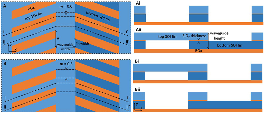
Figure 1. Top-down (A,B) and cross-sectional (Ai,Aii,Bi,Bii) view of partially suspended horizontal-slot fin-waveguide design, demonstrating aligned, m = 0 (A,Ai,Aii) and maximal misaligned, m = 0.5 (B,Bi,Bii) structures.
Two-dimensional finite difference eigenmode simulations were performed to establish field profiles for both high neff TE wire mode and low neff TM slot-mode operation in aligned fin-waveguides. Figure 2 shows linear-scale profiles of |E|, |H|, energy density, and dominant E component (amplitude) for both modes. Ex is the dominant TE electric field component and Ey is the dominant TM magnetic field component. This demonstrates the potential for slot-mode propagation in fin-waveguide devices. Enlarged views of the dominant E-field components for the TE and TM modes at the horizontal slot itself are shown in Figures 2J,K, respectively. This clearly shows E-field enhancement in the slot in TM mode as opposed to TE mode.
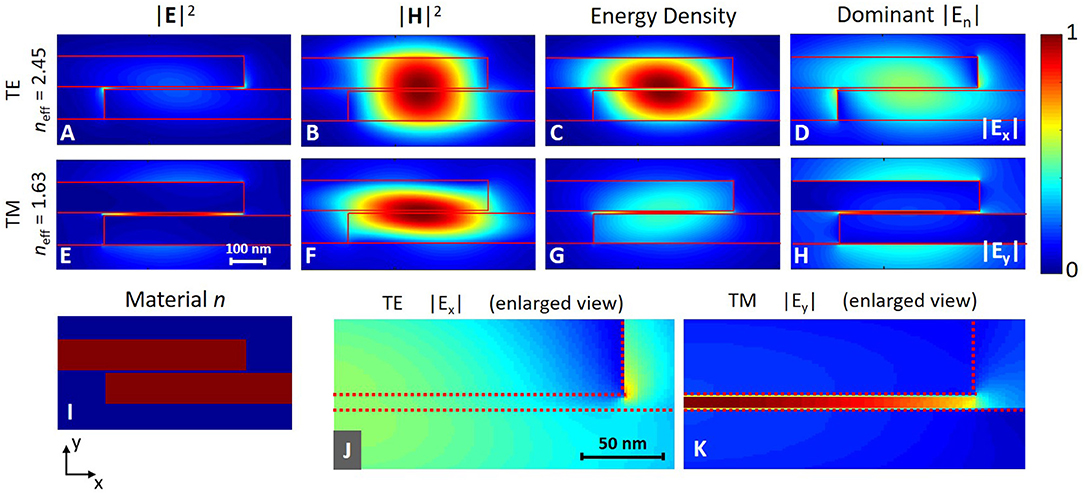
Figure 2. TE and TM mode profiles (normalized, linear-scale) for horizontal-slot fin-waveguide. (A–H) shows the TE (TM) cross-sectional profiles for |E|2, |E|2, energy density and the dominant |En| (|EX| for TE, |EY| for TM) component. Waveguide width = 450 nm. SiO2 cladding (n = 1.44). Fin-waveguide geometry outlined in red. (I) shows the material n profile, where red indicates n = 3.4, blue indicates n = 1.44. (J,K) shows an enlarged view of the dominant electric field component at the waveguide edge for the TE (TM) mode shown in (D,H). For all profiles except (I), max (red) to min (blue) are arbitrary units.
The asymmetric nature of the waveguide leads to the formation of hybridized polarization modes which are neither purely TE nor purely TM. One also expects some degree of diagonal polarization. The degree of linear, diagonal and circular polarization can be determined by calculating the Stokes parameters S1, S2 and S3, respectively, for each polarization field profile [22, 46]. The Stokes parameters at each x, y point can be calculated using the following equations:
Figure 3 shows the relevant Stokes parameters for the quasi-TE and quasi-TM mode profiles. The quasi-TE mode exhibits S1 ~ 0.2 in the central region of the waveguide, which overlaps with the dominant Ex region. The quasi-TM mode exhibits S1 ~ −0.8 in the oxide slot, indicating strong horizontal polarization in the y-direction. The quasi-TE mode exhibits low and negative S2~ values, indicating low diagonal polarization except in the regions either side of the central waveguide region, and the oxide slot, where S2~ peaks at ~−0.2. Similarly, the quasi-TM mode exhibits S2 ~ 0 in most regions, except peaks of S2+− 0.1 at the fin corners, and S2 ~ 0.1 at the center of the slot. This indicates that the quasi-TE and quasi-TM fields have opposite diagonal polarization, and that the regions of highest polarization occur in different regions. This, along with the fact that the dominant E component is identified as overwhelmingly Ex for quasi-TE and Ey for quasi-TM (as shown in Figure 2), justifies our use of the naming convention quasi-TE and quasi-TM modes. These results indicate that the polarizations are physically quasi-TE and quasi-TM.
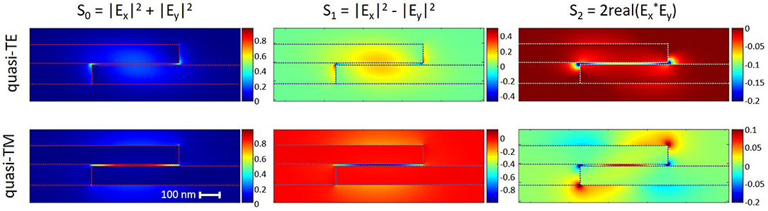
Figure 3. Stokes parameters S0, S1, and S2, for quasi-TE and quasi-TM mode profiles, for horizontal-slot fin-waveguide (outlined with a dotted line).
The dispersion relation for the fin-waveguide design with Λ = 400 nm and fill-factor = 0.5 was calculated using full 3-dimensional FDTD simulations and is presented in Figure 4. Due to band-folding, when m = 0.0 the fundamental odd and even quasi-TE modes (labeled TE1+ and TE1−, respectively) are separated by a 40 nm PBG at the Brillouin zone edge (BZE). The fundamental odd quasi-TM mode (TM1+) crosses with TE1− causing mode degeneracy at normalized frequency (f) = 0.264 (λ = 1,515 nm). The light-line can also be seen and has been labeled for clarity. As m is increased from 0 → 0.5 two phenomena of interest occur simultaneously. The TE1+ and TE1− approach each other at the BZE, coupling and forming a degenerate mode when m = 0.5, and closing the PBG. Also, the TE1− mode splits around the degenerate mode crossing-point TM1+, and can clearly be seen at m = 0.5 coupling with the robust TM1+ at f = 0.269, 0.258 (λ = 1,487, 1,550 nm). This introduces a TE-only bandgap in the middle of the Brillouin zone. At this energy only quasi-TM (slot-mode) is permitted, so it is natural that quasi-TE will couple to quasi-TM at this energy. Mode-splitting by application of lateral-mismatch has been reported in literature for line-defect waveguide planar PhC designs [15, 22, 47, 48], where degenerate, crossed TE1+ and TE1− modes split, but this is the first demonstration of a single mode splitting.
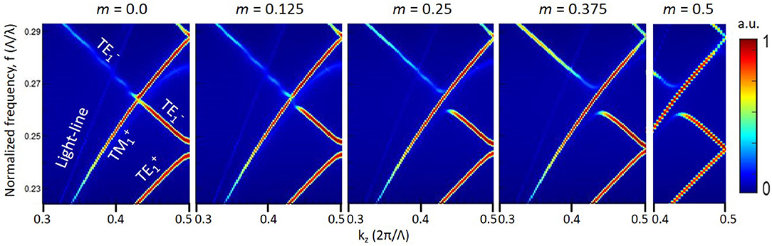
Figure 4. Dispersion relations of horizontal-slot fin-waveguide with mismatch parameter, m = 0.0–0.5. Design: Λ = 400 nm, fill-factor = 0.5.
Figure 5 shows the log-scale |E|, |H|, |P|, |Ey| substrate-normal cut-through profiles at various positions of interest above the BOX for the fully-3D FDTD simulation carried out at m = 0.5, kz = 0.43 * 2πΛ. The fin-waveguide design is Λ = 400 nm, fill-factor = 0.5 and the profiles were extracted at f = 0.264 (λ = 1,517 nm), in the middle of the TE-only bandgap. Profiles are a substrate-normal cut-through of the 400 nm long, 2,600 nm wide simulation region (min-z and max-z Bloch boundary conditions to simulate the periodically repeating structure), at displacements from the BOX/SOI interface which are of particular interest. All four profiles show field distributions across the 3D area of the simulation in accordance with expected slot-mode confinement, for their respective components. The mode dominant component |Ey|, which corresponds to the TM-mode, is shown in Figure 5D to be strongly confined within the 10 nm SiO2 slot, as well as showing minor peaks on the low-n side of both the BOX/SOI and SOI/cladding interfaces. This result is in agreement with the 2D TM mode-profile result presented in Figure 2.
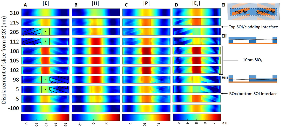
Figure 5. (A–D) |E|, |H|, |P|, |Ey| profiles (log-scale) of guided quasi-TM slot mode from 3D FDTD simulation performed for m = 0.5, kz = 0.43 × 2π/Λ, Λ = 400 nm, fin-width = 200 nm, normalized frequency (f) = 0.264 (λ = 1517 nm). (Ei) Shows the Bloch repeating simulation region (highlighted). (Eii,Eiii) Show the top-fin/bottom-fin waveguide section profile above/below the 10 nm SiO2 layer. The waveguide and fin sidewalls have been overlaid by a black line for the 3rd-4th profile (upper-fin) and 8th-9th profile (lower-fin) of (A).
3. Fabrication
Fabrication of the double-SOI platform and subsequent fin-waveguide structure has been detailed elsewhere [41] and is simply outlined here. Five nanometers thermal oxide was grown on the surface of two (110) crystal-orientation SOI wafers (SOI thickness = 100, 115 nm), which were bonded and thinned creating the double-SOI substrate. Fin-waveguides (aligned and misaligned) as well as input/output waveguides, bends and MMIs, were patterned using electron-beam and conventional inductively coupled plasma (ICP) etching. Local oxidation of silicon (LOCOS) and tetramethylammonium hydroxide (TMAH) anisotropic wet etching was used to under and over-etch the top and bottom fins simultaneously. The left top-fin sidewalls are aligned to the (11-1) crystal plane and act as an etch-stop to TMAH. Due to the mirrored crystal alignment, the same is true of the right bottom-fin sidewalls. The unprotected fin-sidewalls (left-lower and right-upper) are etched. Partially-etched grating couplers (GCs) were defined and ICP etched separately. The structure has an air cladding. The devices were subsequently measured.
Figure 6 shows an SEM image of a fabricated fin-waveguide structure without mismatch (m = 0.0). The image was taken with 54° tilt, which makes the suspension of the top SOI layer fins clearly visible. The periodic bumps protruding from the central section of the waveguide as well as the edge of the fins are caused by semi-stable crystal planes which were not completely removed by the TMAH etching. As these bumps are uniform and periodic across the structure they are not necessarily expected to increase scattering loss. They change the periodic Bragg structure and therefore alter the dispersion relation of the structure, but as they are small compared to the structure overall, they are not expected to significantly affect the nature of the structure or the nature of the quasi-TE to quasi-TM mode conversion. The sharp white lines underneath the suspended left-side fins are the edges of pyramidal semi-stable planes which have not been fully etched. As these are in a region of low EM field intensity according to simulations, they are not expected to significantly effect the performance of the device.
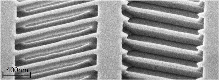
Figure 6. SEM image taken at 54° tilt of aligned (m = 0.0) fin-waveguide structure after ICP etching, TMAH anisotropic etching and oxide removal. The left fins (top SOI layer) are clearly suspended whilst the right fins (bottom SOI layer) have been over-etched.
4. Characterization
The fabrication process is complex and requires significant optimization before it can produce reliably uniform features across a sample area. To account of likely simulation expectation vs. experimental observation “drift” a large search area of device designs was included. In this section we present three sets of devices which demonstrate three phenomena predicted by simulation results presented in Figures 4, 5.
Waveguide device broadband spectra were measured using a TE polarized continuous-wave (CW) tunable (1,525–1,625 nm) laser light source. A fiber polarization controller was used to ensure maximum transmission through TE optimized GC waveguide devices. Light coupled from a single mode fiber into and out of the device using GCs, and transmission power was measured using a photodetector.
Section 4.1 shows the transmission spectra for straight waveguides with Λ = 450 nm, fill-factor = 0.5, m = 0–0.5. Section 4.2 shows the transmission spectra for straight waveguides with Λ = 350 nm, fill-factor = 0.5, m = 0, 0.5. Section 4.3 shows the transmission spectra for an MZI device incorporating a fin-waveguide on one arm, the fin-waveguide having Λ = 450 nm, fill-factor = 0.5, m = 0, 0.25, 0.5. In all of the measured devices the length of the fin-waveguide PhC section was 500 μm long, however, as quasi-TE to quasi-TM conversion relies on bandgap stopping and not adiabatic coupling, mode-beating or self-imaging techniques, and conversion is therefore not dependent on waveguide/device length, the length of the waveguide can be reduced to several μm if desired, massively decreasing device footprint.
4.1. Photonic Bandgap Closing
The simplest experimental demonstration of the phenomenon observed in simulation (Figure 4) is the effect of low-energy PBG shrinking as m → 0.5. This is observed in fin-waveguide design Λ = 450 nm, fill-factor = 0.5. The spectra for these devices are shown in Figure 7. Grating coupler efficiency was measured to be 7 dB/GC at λ = 1,525 nm. The m = 0 fin-waveguide has a PBG width (PBGwidth) ~ 59.94 nm and as m → 0.5 this PBGwidth decreases roughly linearly to 9.98 nm at m = 0.5. Due to the imperfection of the fabrication the PBG does not close completely.
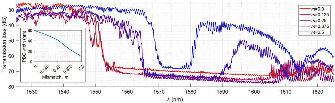
Figure 7. Transmission spectra for 250 μm long horizontal-slot fin-waveguides (Λ = 450 nm, fill-factor = 0.5) at a range of mismatch (m) parameters, demonstrating PBGwidth decreasing linearly as m → 0.5. Inset shows measured PBGwidth as a function of m.
4.2. Straight Waveguide Transverse Magnetic Propagation
High-energy quasi-TE propagation when m = 0, and quasi-TM propagation when m = 0.5, is demonstrated experimentally in a fin-waveguide with Λ = 350 nm, fill-factor = 0.5, which is presented in Figure 8. Figure 8 shows the transmission spectrum (black line) for m = 0 (Ai) and m = 0.5 (Bi). The red to blue lines overlaid onto the transmission spectrum are Gaussian apodizations of the raw spectrum centered at points between λ = 1,540–1,605 nm at 5 nm intervals. The Fourier transform of these normalized spectra produce the λ dependent free-spectral range (λFSR) of that particular section of the spectrum, (Aii) and (Bii) for m = 0 and m = 0.5, respectively.
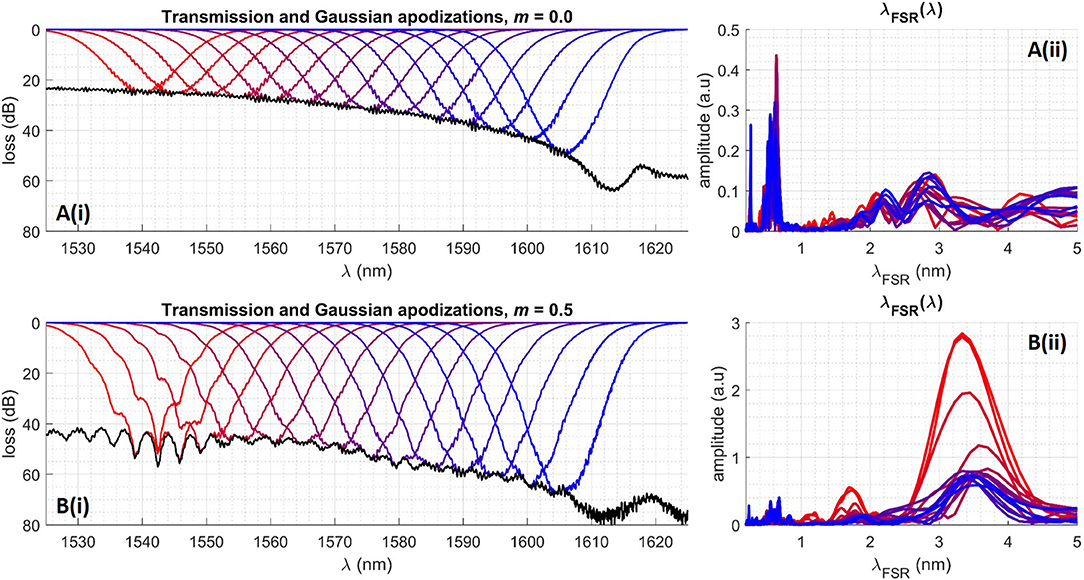
Figure 8. Transmission spectrum (black line) for 250 μm long fin-waveguide (Λ = 350 nm, fill-factor = 0.5) with m = 0.0 (Ai) and m = 0.5 (Bi), with overlaid Gaussian apodized spectra centered on λ = 1,540–1,605 nm (red to blue lines). (Aii,Bii) Show Fourier transforms of Gaussian apodization in (Ai,Bi), which is the precise λFSR of the transmission spectrum as a function of centered λ.
Figure 8Aii for m = 0 exhibits two λFSR peaks, one narrow and “clean” at λFSR = 0.255 nm, the other broad and noisy at λFSR = 0.4–0.7 nm. These peaks can be identified as originating from the GC/GC cavity FPR and the GC/fin-waveguide cavity FPR, respectively. The GC/GC cavity λFSR spectrum is narrow because reflection from the Bragg mirror-like GCs occurs in a narrowly defined space (~15 μm per GC). The λFSR also exhibits a linear dependency on λ. The following equations can be used to extract neff from λFSR in the case of a cavity with consistent neff (Equation 2) and in the case of a cavity with different nefffin components (Equation 3):
Where Lcavity is the length of the cavity, nefffin is the effective refractive index of the fin-waveguide, nefftaper is the refractive index of the taper, Ltaper is the length of the taper, and Lfin is the length of the fin-waveguide.
Due to the fabrication non-uniformity, the fin-waveguide/wire-waveguide interface is not operating as a single reflection point, therefore the λFSR is broadened. The broad λFSR spectrum peaks in Figure 8Aii at λFSR = 0.6 nm indicate a neff = 3.94 in the 500 μm taper-waveguide (Equation 2). Using nefftaper= 3.94, Ltaper = 1 mm, Lfin = 250 μm, we can calculate nefffin = 3.17. This is only an approximate value as there is large uncertainty in λFSR.
Figure 8Bi shows that with m = 0.5 the spectrum pattern is altered significantly in the high-energy region. Figure 8Bii shows two λFSR peaks that are not present in (Aii). The major peak occurs at λFSR = 3.33 nm for Gaussian apodization centered on 1,540 nm. Using Equation (3) this gives a nefffin = 1.42. The minor peak occurs at λFSR = 1.7 nm for Gaussian apodization also centered on 1,540 nm. Using Equation (3) this gives a nefffin = 2.79. This implies that at high-energy this particular mismatched fin-waveguide is multi-mode, supporting a dominant quasi-TM slot-mode (indicated by the large λFSR = 3.33 nm peak) as well as a less dominant quasi-TE strip-mode. The fact that large λFSR amplitude peaks are present indicates that the coupling between the strip-waveguide/fin-waveguide is poor, and a large proportion of the light is being reflected. However, despite this, the clear λFSR = 3.33 nm peak associated with quasi-TM cavity FPR demonstrates that a 10 nm slot-mode has been induced by the application of m = 0.5, and the nefffin = 1.42.
4.3. Mach-Zehnder Interferometer Transverse Magnetic Propagation
Figure 9 shows the transmission spectra, Fourier transform calculated λFSR(λ), and neff(λ) for three asymmetric MZI devices (ΔLarm = 542 μm) with different 500 μm long waveguide designs on one arm; (Ai–iv) is a strip-waveguide reference device with a strip-waveguide on both arms, (Bi–iv), is a fin-waveguide reference device with a m = 0.0 fin-waveguide on one arm, and (Ci–iv) is an MZI incorporating a m = 0.5 fin-waveguide on one arm. Figure 9Ai shows a typical MZI transmission spectrum with λFSR(λ) linearly increasing from 0.92 to 1.03 nm from λ = 1,535–1,600 nm (Aii and Aiii). This corresponds to neff decreasing linearly from 2.37 to 2.29 (Aiv). The linear decrease in neff and lack of sharp discontinuity across λ indicates that the same mode (quasi-TE) is propagating across the spectrum. Similarly, (Bi) shows a typical MZI transmission spectrum with λFSR(λ) linearly increasing from 0.99 to 1.14 nm from λ = 1,535–1,600 nm (Bii and Biii) which corresponds to neff decreasing linearly from 2.2 to 2.08 (Biv). This indicates that the m = 0.0 fin-waveguide is operating in quasi-TE mode, irrespective of λ.
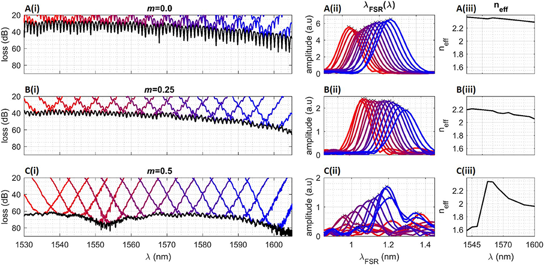
Figure 9. Transmission spectrum (black) with overlaid Gaussian apodized spectra centered on λ = 1,540–1,605 nm (red to blue lines) for a MZI device [(ΔLarm) = 542 μm] incorporating on the “active” arm a strip-waveguide (Ai), a m = 0.0 fin-waveguide (Bi), or a m = 0.5 fin-waveguide (Ci). λFSR for each Gaussian apodized spectrum in the corresponding device are shown in (Aii,Bii,Cii). (Aiii,Biii,Ciii) Show the calculated neff(λ) based on corresponding λFSR.
If the propagating mode changes from quasi-TE to quasi-TM as a function of λ within the 500 μm long waveguide on one of the arms, we expect to see a change in the λFSR(λ), and therefore a change in the neff(λ). This is indeed what we can observe in the transmission data for the asymmetric MZI device incorporating a fin-waveguide (Δ = 450 nm, fill-factor = 0.5, m = 0.5) (Figure 9Ci). Because of the high-loss associated with m = 0.5 devices the transmission spectrum exhibits high noise, the λFSR peaks extracted from the Gaussian-apodized spectrum are broader than those extracted from the reference data. However, λFSR can still be identified in Figure 9Cii, particularly for λ = 1,555–1,600 nm, with a linear increase in λFSR from 0.95 → 1.2 nm. λFSR can also be identified for Gaussian-normalizations centered on lower wavelengths, most notably for λ = 1,535 nm, where λFSR = 1.37. Figure 9Cii shows that for Gaussian-apodization centered on 1,540, 1,545, and 1,550 nm, λFSR = 1.35, 1.33, 1.11 nm, respectively. λFSR as a function of centered λ therefore begins at λFSR = 1.37 nm, decreases with a sharp discontinuity to 0.95 nm as λ increases, and then increases linearly as a function of λ. Figure 9Ciii shows the effect on neff(λ). Between λ = 1,535–1,545 nm neff = 1.57–1.65, and at λ = 1,555 nm neff = 2.34. Despite the fact that the transmission and λFSR spectra exhibit high noise, this is clear evidence that the neff (Ciii) is highly dependent on λ in a discontinuous, non-linear way. This is explained by the dominance of the 10 nm slot quasi-TM mode propagation within the mismatched fin-waveguide at low λ, and standard quasi-TE mode propagation at higher λ.
5. Conclusion
In this paper we have experimentally demonstrated quasi-TE to quasi-TM mode conversion through the introduction of a lateral mismatch to an asymmetric fin-waveguide PhC. Transmission spectra demonstrate non-linear dependence of λ on neff for two mismatched fin-waveguide devices, with neff being calculated to be between 1.37–1.42 at low-λ and 2.75–3.94 at high-λ. neff = 1.37–1.42 at low-λ is evidence of quasi- TM propagation within the 10 nm thick horizontal oxide slot region. This is the narrowest oxide-slot TM propagation currently reported in literature. 3D FDTD simulations predict that as m → 0.5, the TE1− band splits within the Brillouin zone, whilst the TE1+ remains robust and unaffected. The loss associated with mismatched fin-waveguides is currently high, but once the fabrication process is optimized, these devices will be useful in sensing, light-amplification, modulation, and other telecommunication applications requiring very narrow TM slot-mode propagation. TE/TM dispersion relation engineering through the utilization of a lateral mismatch in an asymmetric geometry can also be developed, based on these proof-of-concept designs and demonstrations, to explore new ways of manipulating light, adding a new degree of freedom to PhC design.
Data Availability Statement
The datasets presented in this study can be found in online repositories. The names of the repository/repositories and accession number(s) can be found at: https://doi.org/10.5258/SOTON/D1607.
Author Contributions
JB conceived of the idea with the help of ideas presented by HA and wrote the manuscript. MS contributed the simulation code, which JB implemented. JB, MH, and KK fabricated the devices. KD took the SEM image. Devices were measured in optical measurement labs setup and maintained by DT and GR. MC provided the guidance. SS provided the significant guidance during design, fabrication, analysis, and manuscript writing. JH provided the help with manuscript preparation. All authors were involved in the revision of the manuscript.
Funding
This work was supported by the EPSRC Standard Grant (EP/M009416/1), EPSRC Standard Grant (EP/S034242/1), EPSRC Manufacturing Fellowship (EP/M008975/1), EPSRC Platform Grant (EP/N013247/1), and The University of Southampton Zepler Institute Research Collaboration Stimulus Fund. DT acknowledges funding from the Royal Society for his University Research Fellowship.
Conflict of Interest
HA was employed by Research and Development Group Hitachi, Ltd.
The remaining authors declare that the research was conducted in the absence of any commercial or financial relationships that could be construed as a potential conflict of interest.
References
1. Yablonovitch E, Gmitter T. Photonic band structure: the face-centered-cubic case. Phys Rev Lett. (1989) 63:1950. doi: 10.1103/PhysRevLett.63.1950
2. Satpathy S, Zhang Z, Salehpour M. Theory of photon bands in three-dimensional periodic dielectric structures. Phys Rev Lett. (1990) 64:1239. doi: 10.1103/PhysRevLett.64.1239
3. Leung KM, Liu Y. Full vector wave calculation of photonic band structures in face-centered-cubic dielectric media. Phys Rev Lett. (1990) 65:2646. doi: 10.1103/PhysRevLett.65.2646
4. Zhang Z, Satpathy S. Electromagnetic wave propagation in periodic structures: Bloch wave solution of Maxwell's equations. Phys Rev Lett. (1990) 65:2650. doi: 10.1103/PhysRevLett.65.2650
5. Hill K, Fujii Y, Johnson DC, Kawasaki B. Photosensitivity in optical fiber waveguides: application to reflection filter fabrication. Appl Phys Lett. (1978) 32:647–9. doi: 10.1063/1.89881
6. Baba T, Fukaya N, Yonekura J. Observation of light propagation in photonic crystal optical waveguides with bends. Electron Lett. (1999) 35:654–5. doi: 10.1049/el:19990438
7. Smith C, Benisty H, Olivier S, Rattier M, Weisbuch C, Krauss T, et al. Low-loss channel waveguides with two-dimensional photonic crystal boundaries. Appl Phys Lett. (2000) 77:2813–5. doi: 10.1063/1.1322367
8. Lončar M, Nedeljković D, Doll T, Vučković J, Scherer A, Pearsall TP. Waveguiding in planar photonic crystals. Appl Phys Lett. (2000) 77:1937–9. doi: 10.1063/1.1311604
9. Bogaerts W, Baets R, Dumon P, Wiaux V, Beckx S, Taillaert D, et al. Nanophotonic waveguides in silicon-on-insulator fabricated with CMOS technology. J Lightw Technol. (2005) 23:401–12. doi: 10.1109/JLT.2004.834471
10. Noda S, Tomoda K, Yamamoto N, Chutinan A. Full three-dimensional photonic bandgap crystals at near-infrared wavelengths. Science. (2000) 289:604–6. doi: 10.1126/science.289.5479.604
11. Blanco A, Chomski E, Grabtchak S, Ibisate M, John S, Leonard SW, et al. Large-scale synthesis of a silicon photonic crystal with a complete three-dimensional bandgap near 1.5 micrometres. Nature. (2000) 405:437–40. doi: 10.1038/35013024
12. Letartre X, Seassal C, Grillet C, Rojo-Romeo P, Viktorovitch P, Le Vassor d'Yerville M, et al. Group velocity and propagation losses measurement in a single-line photonic-crystal waveguide on InP membranes. Appl Phys Lett. (2001) 79:2312–4. doi: 10.1063/1.1405146
13. Vlasov YA, O'boyle M, Hamann HF, McNab SJ. Active control of slow light on a chip with photonic crystal waveguides. Nature. (2005) 438:65–9. doi: 10.1038/nature04210
14. Baba T. Slow light in photonic crystals. Nat Photon. (2008) 2:465–73. doi: 10.1038/nphoton.2008.146
15. Sotto M, Debnath K, Khokhar AZ, Tomita I, Thomson D, Saito S. Anomalous zero-group-velocity photonic bonding states with local chirality. J Opt Soc Am B. (2018) 35:2356–63. doi: 10.1364/JOSAB.35.002356
16. Ryu HY, Notomi M, Lee YH. High-quality-factor and small-mode-volume hexapole modes in photonic-crystal-slab nanocavities. Appl Phys Lett. (2003) 83:4294–6. doi: 10.1063/1.1629140
17. Song BS, Noda S, Asano T, Akahane Y. Ultra-high-Q photonic double-heterostructure nanocavity. Nat Mater. (2005) 4:207–10. doi: 10.1038/nmat1320
18. Deotare PB, McCutcheon MW, Frank IW, Khan M, Lončar M. High quality factor photonic crystal nanobeam cavities. Appl Phys Lett. (2009) 94:121106. doi: 10.1063/1.3107263
19. Rao VM, Hughes S. Single quantum-dot Purcell factor and β factor in a photonic crystal waveguide. Phys Rev B. (2007) 75:205437. doi: 10.1103/PhysRevB.75.205437
20. Arcari M, Söllner I, Javadi A, Hansen SL, Mahmoodian S, Liu J, et al. Near-unity coupling efficiency of a quantum emitter to a photonic crystal waveguide. Phys Rev Lett. (2014) 113:093603. doi: 10.1103/PhysRevLett.113.093603
21. Chen XD, Zhao FL, Chen M, Dong JW. Valley-contrasting physics in all-dielectric photonic crystals: orbital angular momentum and topological propagation. Phys Rev B. (2017) 96:020202. doi: 10.1103/PhysRevB.96.020202
22. Sotto M, Debnath K, Tomita I, Saito S. Spin-orbit coupling of light in photonic crystal waveguides. Phys Rev A. (2019) 99:053845. doi: 10.1103/PhysRevA.99.053845
23. Zhang X, Hosseini A, Chakravarty S, Luo J, Jen AKY, Chen RT. Wide optical spectrum range, subvolt, compact modulator based on an electro-optic polymer refilled silicon slot photonic crystal waveguide. Opt Lett. (2013) 38:4931–4. doi: 10.1364/OL.38.004931
24. Vogelbacher F, Sagmeister M, Kraft J, Zhou X, Huang J, Li M, et al. Slot-waveguide silicon nitride organic hybrid distributed feedback laser. Sci Rep. (2019) 9:18438. doi: 10.1038/s41598-019-54655-4
25. Almeida VR, Xu Q, Barrios CA, Lipson M. Guiding and confining light in void nanostructure. Opt Lett. (2004) 29:1209–11. doi: 10.1364/OL.29.001209
26. Xu Q, Almeida VR, Panepucci RR, Lipson M. Experimental demonstration of guiding and confining light in nanometer-size low-refractive-index material. Opt Lett. (2004) 29:1626–8. doi: 10.1364/OL.29.001626
27. Baehr-Jones T, Hochberg M, Wang G, Lawson R, Liao Y, Sullivan PA, et al. Optical modulation and detection in slotted silicon waveguides. Opt Express. (2005) 13:5216–26. doi: 10.1364/OPEX.13.005216
28. Sun R, Dong P, Feng N, Hong C, Michel J, Lipson M, et al. Horizontal single and multiple slot waveguides: optical transmission at λ = 1550 nm. Opt Express. (2007) 15:17967–72. doi: 10.1364/OE.15.017967
29. Koos C, Vorreau P, Vallaitis T, Dumon P, Bogaerts W, Baets R, et al. All-optical high-speed signal processing with silicon-organic hybrid slot waveguides. Nat Photon. (2009) 3:216–9. doi: 10.1038/nphoton.2009.25
30. Dutta HS, Goyal AK, Srivastava V, Pal S. Coupling light in photonic crystal waveguides: a review. Photon Nanostruct Fundam Appl. (2016) 20:41–58. doi: 10.1016/j.photonics.2016.04.001
31. Wu X, Dama B, Gothoskar P, Metz P, Shastri K, Sunder S, et al. A 20Gb/s NRZ/PAM-4 1V transmitter in 40 nm CMOS driving a Si-photonic modulator in 0.13 μm CMOS. In: Solid-State Circuits Conference Digest of Technical Papers (ISSCC). San Francisco, CA: IEEE (2013). p. 128–9. doi: 10.1109/ISSCC.2013.6487667
32. Webster M, Gothoskar P, Patel V, Piede D, Anderson S, Tummidi R, et al. An efficient MOS-capacitor based silicon modulator and CMOS drivers for optical transmitters. In: 2014 IEEE 11th International Conference on Group IV Photonics (GFP). Paris: IEEE (2014). p. 1–2. doi: 10.1109/Group4.2014.6961998
33. Sodagar M, Hosseinnia AH, Isautier P, Moradinejad H, Ralph S, Eftekhar AA, et al. Compact, 15 Gb/s electro-optic modulator through carrier accumulation in a hybrid Si/SiO2/Si microdisk. Opt Express. (2015) 23:28306–15. doi: 10.1364/OE.23.028306
34. Moradinejad H, Atabaki AH, Hosseinia AH, Eftekhar AA, Adibi A. High-Q resonators on double-layer SOI platform. In: 2013 Photonics Conference (IPC). Seattle: IEEE (2013). p. 430–1. doi: 10.1109/IPCon.2013.6656621
35. Qi B, Yu P, Li Y, Hao Y, Zhou Q, Jiang X, et al. Ultracompact electrooptic silicon modulator with horizontal photonic crystal slotted slab. IEEE Photon Technol Lett. (2010) 22:724–6. doi: 10.1109/LPT.2010.2044878
36. Kim Y, Lee YJ, Hong S, Moon K, Kwon SH. Photonic crystal cavity with a thin low-index layer for silicon-compatible nanolight source. Appl Sci. (2018) 8:1552. doi: 10.3390/app8091552
37. Lin CY, Wang AX, Lai WC, Covey JL, Chakravarty S, Chen RT. Coupling loss minimization of slow light slotted photonic crystal waveguides using mode matching with continuous group index perturbation. Opt Lett. (2012) 37:232–4. doi: 10.1364/OL.37.000232
38. Deng Q, Liu L, Li X, Zhou Z. Strip-slot waveguide mode converter based on symmetric multimode interference. Opt Lett. (2014) 39:5665–8. doi: 10.1364/OL.39.005665
39. Debnath K, Thomson DJ, Zhang W, Khokhar AZ, Littlejohns C, Byers J, et al. All-silicon carrier accumulation modulator based on a lateral metal-oxide-semiconductor capacitor. Photon Res. (2018) 6:373–9. doi: 10.1364/PRJ.6.000373
40. Debnath K, Thomson DJ, Zhang W, Khokhar AZ, Littlejohns C, Byers J, et al. 20Gbps silicon lateral MOS-Capacitor electro-optic modulator. In: CLEO: Science and Innovations. San Jose: Optical Society of America (2018). p. SM3B-5. doi: 10.1364/CLEO_SI.2018.SM3B.5
41. Byers J, Debnath K, Arimoto H, Husain MK, Sotto M, Li Z, et al. Silicon slot fin waveguide on bonded double-SOI for a low-power accumulation modulator fabricated by an anisotropic wet etching technique. Opt Express. (2018) 26:33180–91. doi: 10.1364/OE.26.033180
42. Hutchings DC, Holmes BM. A waveguide polarization toolset design based on mode beating. IEEE Photon J. (2011) 3:450–61. doi: 10.1109/JPHOT.2011.2146765
43. Holmes BM, Hutchings DC. Realization of novel low-loss monolithically integrated passive waveguide mode converters. IEEE Photon Technol Lett. (2006) 18:43–5. doi: 10.1109/LPT.2005.859987
44. Vermeulen D, Selvaraja S, Verheyen P, Absil P, Bogaerts W, Van Thourhout D, et al. Silicon-on-insulator polarization rotator based on a symmetry breaking silicon overlay. IEEE Photon Technol Lett. (2012) 24:482–4. doi: 10.1109/LPT.2011.2181944
45. Xie A, Zhou L, Chen J, Li X. Efficient silicon polarization rotator based on mode-hybridization in a double-stair waveguide. Opt Express. (2015) 23:3960–70. doi: 10.1364/OE.23.003960
46. Ren ZC, Kong LJ, Li SM, Qian SX, Li Y, Tu C, et al. Generalized poincaré sphere. Opt Express. (2015) 23:26586–95. doi: 10.1364/OE.23.026586
47. Mock A, Lu L, O'Brien J. Space group theory and Fourier space analysis of two-dimensional photonic crystal waveguides. Phys Rev B. (2010) 81:155115. doi: 10.1103/PhysRevB.81.155115
Keywords: silicon photonics, slot-mode, polarization conversion, misaligned photonic crystal, double-SOI, anisotropic wet etching
Citation: Byers J, Debnath K, Arimoto H, Husain MK, Sotto M, Hillier J, Kiang K, Thomson DJ, Reed GT, Charlton M and Saito S (2021) 10 nm SiO2 TM Slot Mode in Laterally Mismatched Asymmetric Fin-Waveguides. Front. Phys. 9:659585. doi: 10.3389/fphy.2021.659585
Received: 27 January 2021; Accepted: 15 April 2021;
Published: 27 May 2021.
Edited by:
Bodo Wilts, Université de Fribourg, SwitzerlandReviewed by:
Tatiana S. Perova, Trinity College Dublin, IrelandDavid C. Hutchings, University of Glasgow, United Kingdom
Copyright © 2021 Byers, Debnath, Arimoto, Husain, Sotto, Hillier, Kiang, Thomson, Reed, Charlton and Saito. This is an open-access article distributed under the terms of the Creative Commons Attribution License (CC BY). The use, distribution or reproduction in other forums is permitted, provided the original author(s) and the copyright owner(s) are credited and that the original publication in this journal is cited, in accordance with accepted academic practice. No use, distribution or reproduction is permitted which does not comply with these terms.
*Correspondence: James Byers, Si5CeWVyc0Bzb3Rvbi5hYy51aw==