 Stavros Giannakopoulos1,2*
 Ilias Sourikopoulos1
 Leontios Stampoulidis1
 Pylyp Ostrovskyy3
 Florian Teply3K. Tittelbach-Helmrich3Goran Panic3Gunter Fischer3
 Alexander Grabowski4Herbert Zirath2Philippe Ayzac5Norbert Venet5Anaëlle Maho5Michel Sotom5
 Shaun Jones6Grahame Wood6Ian Oxtoby6
- 1LEO Space Photonics R&D, Athens, Greece
- 2Microwave Electronics Laboratory, Department of Microtechnology and Nanoscience (MC2), Chalmers University of Technology, Gothenburg, Sweden
- 3IHP - Leibniz-Institut für innovative Mikroelektronik, Frankfurt, Germany
- 4Photonics Laboratory, Department of Microtechnology and Nanoscience (MC2), Chalmers University of Technology, Gothenburg, Sweden
- 5Thales Alenia Space, Toulouse, France
- 6ALTER TECHNOLOGY TÜV NORD UK Ltd., Livingston, United Kingdom
We report the design of a 112 Gb/s radiation-hardened (RH) optical transceiver applicable to intra-satellite optical interconnects. The transceiver chipset comprises a vertical-cavity surface-emitting laser (VCSEL) driver and transimpedance amplifier (TIA) integrated circuits (ICs) with four channels per die, which are adapted for a flip-chip assembly into a mid-board optics (MBO) optical transceiver module. The ICs are designed in the IHP 130 nm SiGe BiCMOS process (SG13RH) leveraging proven robustness in radiation environments and high-speed performance featuring bipolar transistors (HBTs) with fT/fMAX values of up to 250/340 GHz. Besides hardening by technology, radiation-hardened-by-design (RHBD) components are used, including enclosed layout transistors (ELTs) and digital logic cells. We report design features of the ICs and the module, and provide performance data from post-layout simulations. We present radiation evaluation data on analog devices and digital cells, which indicate that the transceiver ICs will reliably operate at typical total ionizing dose (TID) levels and single event latch-up thresholds found in geostationary satellites.
Introduction
Satellite operators expect the telecommunication satellite industry to deliver ever more efficient systems solutions to reduce the cost per bit on orbit and to improve their own service offering. A brand new class of very/high throughput satellites (V/HTSs) is thus being developed that pushes the next frontier in the terabit/s range and will be delivered from now on. A V/HTS relies on sophisticated antenna coverage based on extensive frequency reuse and many narrow spot beams. Migration to higher frequencies (Ka, Q/V, W…) makes larger bandwidth available. V/HTS solutions are designed to support flexibility in various aspects: coverage, connectivity, frequency plan and channelization, bandwidth, and power allocation. Basically, a V/HTS must be able to deliver the required capacity where and when needed. It must also be able to serve various and evolving demands [1].
Satellite manufacturers are, therefore, augmenting onboard processing capabilities in both capacity and flexibility, benefiting from advances in integration, speed, interfaces, and power dissipation of state-of-the-art qualified microelectronic components. Thales Alenia Space has developed the so-called digital transparent processor (DTP) product family. As shown in Figure 1, DTPs have analog-to-digital converters (ADCs) and digital-to-analog converters (DACs) at their input and output interfaces and make full use of digital processing inside to provide fully flexible connectivity and programmable bandwidth allocation. They are particularly well-suited for routing radio frequency (RF) channels or sub-channels with fine granularity of bandwidth in missions with numerous antenna beams. Digital beam forming (DBF) can also be supported, which not only allows the formation of multiple beams simultaneously but becomes very attractive for missions that require reconfiguration of the antenna coverage.
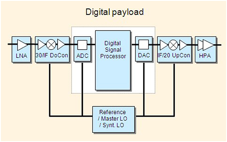
Figure 1. Functional architecture of a digital processor-based telecom payload.
However, accommodating such large payloads on satellite platforms with their size, weight, and power (SWaP) consumption constraints still remains a significant challenge. In the conviction that photonic interconnects have a great potential to meet the expectations of scaling payloads to very high throughputs while maintaining accepted SWaP, Thales Alenia Space was the first prime company to go through the full cycle from conceptual design to hardware demonstration and up to flight-grade equipment development. Thales Alenia Space has qualified the DTP product based on state-of-the-art enabling technologies, namely, deep submicron application-specific integrated circuit (ASIC) and optical interconnects at high data rates. More specifically, optical technology was introduced within the Spaceflex™ VHTS product (DTP-5G) that enabled total capacities of 480 GHz, which was 1,500 times higher than those of the first generation deployed in 2006. Optical interconnects become the technology of choice for conveying huge amounts of data generated within digital payload systems. Nevertheless, the overall capacity of future payloads remains bounded by the overall SWaP at satellite level, so that lowering power consumption will increasingly drive the design of any advanced digital payload.
The unique challenges of the space environment, such as temperature cycling, constant bombardment by high energy particles, and no possibility for repair are setting strict requirements for intra-satellite optical communication links [2]. High data rate, multichannel GaAs VCSEL-based optical fiber links are enabled by advances in VCSEL components [3] and established standards, such as SpaceFibre [4]. At data rates >10 Gb/s, VCSEL-based fiber optical links are preferred because of lower power consumption, smaller footprint, and, especially, higher technology readiness level (TRL) [5], when compared with other alternatives, such as wireless optical and silicon photonics-based links. The state-of-the-art literature presents a 4 × 10 Gbps ASIC VCSEL-based transceiver operating on the “SpaceFibre” standard demonstrated by Karppinen et al. [6]. Additionally, Ko et al. demonstrated a 3 × 25 Gbps VCSEL-based transceiver ASIC with separate 3 × 25 single-ended receiver and 3 × 25 single-ended transmitter sub-assemblies [7], which was subsequently integrated into a 6 × 25 Gbps module [8].
Onboard optical transceivers currently operate on 12.5 Gb/s lanes. However, the next generations are calling for line rates >25 Gb/s or even 56 Gb/s to better fit with the high-speed hardened ASIC technology that will become available. The major typical requirements put to optical interconnect solutions for future digital payloads are given in Table 1. As the ASIC technology improves, the contribution of transceivers to power consumption becomes more critical in optically connected digital payloads. As a result, optical transceivers become a key component that must operate at a data rate >25 Gb/s with the ability to scale to 56 Gb/s and reduce their power consumption below 10 mW/Gb/s. It is equally important is that the electronics inside a transceiver is radiation-resistant (RR) and manufactured with a technology node that will allow for future-proof scalability of data rates and power. Table 2 presents some key metrics that govern digital transceiver performance. Figure 2, as shown below, illustrates the impact of such parameters. The theoretical bit error rate (BER) curves are plotted for 25 Gb/s on-off keying (OOK) transmission with different values for extinction ratio (ER), laser relative intensity noise (RIN), and thermal noise density.
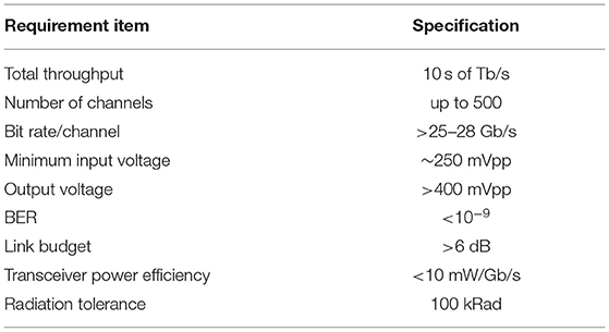
Table 1. Top-level requirements for payload digital transceivers.
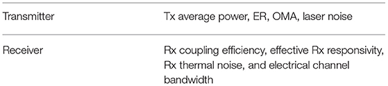
Table 2. Key metrics for transceiver.
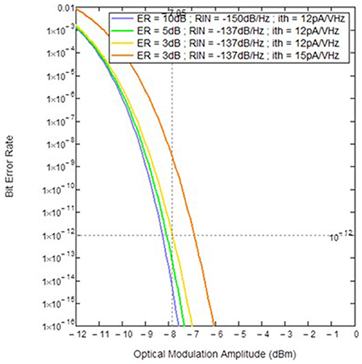
Figure 2. Estimated BER performance of an on-off keying 25 Gb/s transmission for different values of ER, RIN, and thermal noise density (effective Rx responsivity = 0.14 A/W).
A preliminary optical link budget is given below considering worst case and typical scenarios. For the space application several losses have to be taken into account in order to ensure End-of-life performance, such as transmitter aging, radiation-induced losses and bend losses. These losses will define the required minimum transmitter output power and ER to meet the target receiver sensitivity.
After summarizing system-level requirements, we can proceed to presenting the design features of the implementing hardware, namely, a mid-board optical transceiver comprising of a VCSEL driver and a TIA chipset capable of 112 Gb/s transmission. The rest of this report is organized as follows: first, in section Optical Sub-assembly Design, we present packaging aspects with the design of the host optical module. We performed electrical and optical simulations to address performance requirements. In section Radiation Hardening Requirements and Process Technology, we provide an overview of radiation hardening requirements and comment on targeted process technology. The implementation of the VCSEL driver IC will be reported in section Vertical-Cavity Surface-Emitting Laser Driver Design, and the TIA IC in section Transimpedance Amplifier IC Circuit. We conclude this study in the last section.
Optical Sub-Assembly Design
For a digital payload system where the density of I/Os becomes important, a pluggable mid-board embedded optics solution provides the form factor required that can enable populating the host printed circuit board (PCB) to reach the required capacity. The optical sub-assembly (OSA) transceiver developed for this project is a mid-board optical module that utilizes a borosilicate glass carrier, which provides the means for optical waveguiding and the substrate for electrical routing at the same time. The transmitter part comprises a four-channel VCSEL driver and a quad VCSEL array, and the receiver part includes a four-channel transimpedance amplifier and quad photodiode array ICs.
The PCB inside the module acts as an interposer that provides the electrical interface between the OSA and the on-board MEC5-RA connector (Samtec1, New Albany, IN, United States). This is a right-angle, double-row, 60-pin connector that is compatible with the Consortium for On-board Optics (COBO)2 specification. It ensures the necessary performance for multi-Gb/s operation and provides the facility of a pluggable solution. The fiber assembly of the module comprises a V-groove array of multimode fibers mated to a multichannel MT ferrule. Functional diagrams of the transceiver module and CAD rendering are shown in Figures 3A,B, respectively. The module size is 17 × 38.42 × 7.2 mm.
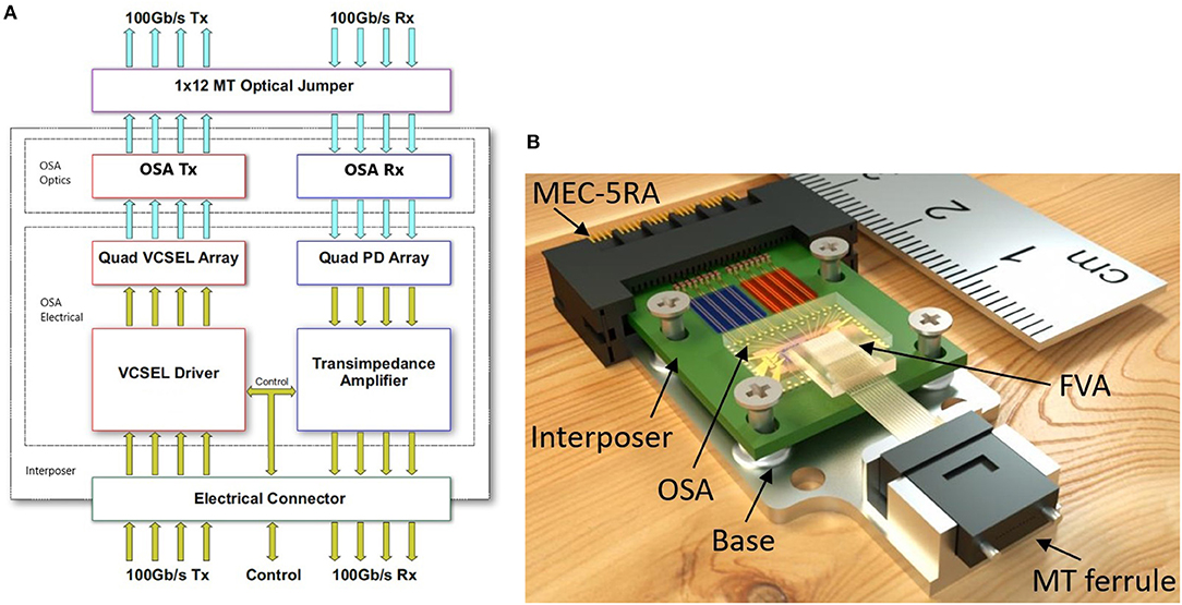
Figure 3. (A) Functional diagram and (B) CAD rendering of the mid-board optical transceiver module [9].
The flip-chip process is one of the key assembly processes for hosted ICs and optical parts that ensure high-speed performance with minimum parasitic elements. Electrical simulations were carried out based on electromagnetic (EM) modeling of all parts of the package. In addition to that, four differential RF lines from the TIA/VCSEL driver to the contact pads of the connector were also modeled. The technology profile includes the OSA to interposer connection via stud bumps, solder mask resist on the PCB, polyimide layers of the OSA, and underfill of the stud bump connections. The S-parameter simulation results for insertion loss and return loss are shown in Figures 4A,B, respectively.
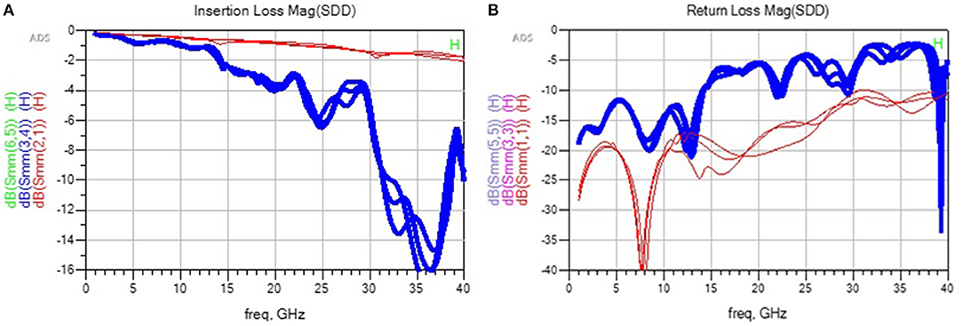
Figure 4. Package EM model results. (A) S-parameter simulations for insertion loss and (B) return loss for the RF signal path with (blue) and without (red) the module external connector.
The insertion loss for the RF path without the external connector is < -3 dB up to 40 GHz, where the frequency response is flat and has no resonance dips. The return loss was found to be < -15 dB up to 25 GHz and < -10 dB up to 40 GHz. When the connector is included, the insertion loss for the RF path was found to be < -3 dB up to 16 GHz. This shows the criticality of the connector interface in the signal path. Nevertheless, this performance is adequate for a 28-Gb/s operation per lane. The transceiver module was designed to optionally accommodate a re-timing electronic IC element in the case of stringent system conditions.
It is important to mention that careful thermal analysis and design were conducted to address deployment settings, as temperature plays a key role in laser performance and related optical power. The operating temperature for the module has been determined to be from −40 to 85°C, following the requirements for the VCSEL. Moreover, detailed optical modeling was performed to ensure that coupling losses for the VCSEL and photodiode fiber interfaces would remain below the specified levels.
The design and fabrication of the VCSEL driver and TIA receiver ICs have been conducted based on the functional specification shown in Table 3. Physical design in terms of die dimensions and pad outline were specified in advance and incorporated early into the module specification. This allowed the development efforts for the module and ICs to be carried out in parallel.
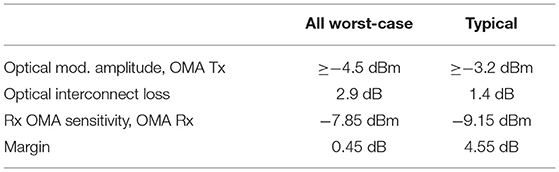
Table 3. On-off keying 25 Gb/s optical link budget.
Radiation Hardening Requirements and Process Technology
Two types of effects affect IC functionality in the space environment: cumulative and single event effects (SEEs). Cumulative effects are caused by long-term exposure of electronics to radiation and expressed by total ionizing dose (TID) and total non-ionizing dose (TNID). SEEs refer to effects that occur when an ionizing particle hits an IC and might influence its performance [10].
Requirements on radiation hardness of ASICs should be derived from several aspects of a space mission: acceptable performance, external radiation sources, and shielding. Assuming a satellite position at the geostationary orbit (GEO), we determine corresponding limits in terms of SEEs and TID.
At the given orbit, galactic cosmic rays (GCRs) are the major source of SEEs. As GCR flux spectra are also modulated by the activity of the sun, we deliberately chose a mission section during solar minimum as a guiding reference. Another reasonable assumption is that the electronics to be designed here are located inside the outer shell of a spacecraft; therefore, they will be enclosed by some structural parts of the spacecraft. We estimate this to be equivalent to 0.5 mm of aluminum. Based on these assumptions, we have chosen an ISO 15390 GCR model [11] for a solar minimum in the GEO orbit, and calculated the effective linear energy transfer (LET) spectrum after passing through 0.5 mm of aluminum. The analysis has shown that the aluminum shielding alters mainly the low-energy part of the particle spectrum and does not contribute appreciably to the SEE hardness of the system at the GEO orbit. Figure 5 shows the resulting limits for system-level cross-section to achieve a soft error rate of 1/day. Thicker shielding of up to a few millimeters does not change the results significantly.
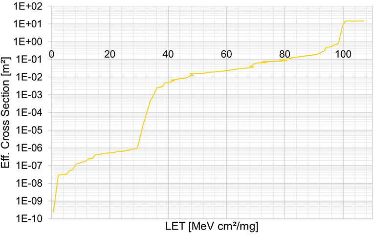
Figure 5. Allowable system-level cross-section depending on particle LET at the GEO orbit.
For the TID requirement, there is no need to perform any particular simulations, as corresponding data are already available in Evans [12]. Assuming 15 years of operation, ASICs must withstand a TID of 100 kRad, if placed in a satellite with 5 mm of Al shielding.
For the TIA and VCSEL driver IC design and fabrication, an IHP 0.13 μm SiGe BiCMOS semiconductor process has been chosen. This process offers high-performance npn-HBTs demonstrating fT/fMAX values of up to 250/340 GHz, which are well-suited to achieve a 28-Gb/s operation per channel or even more [13], having a substantial speed margin for scalability. At the same time, the chosen technology has already been evaluated for radiation hardness [14], so the SiGe HBTs demonstrated high resistance to TID doses, achieving TID levels as high as 1.2 MRad. For the digital circuits, there are 3.3 V I/O CMOS and 1.2 V standard CMOS libraries available, and an RH digital library that includes RH flip-flops operating up to a LET of 62 MeVcm2/mg without any single-event upset occurrence. Up to the same LET value, all RH standard cells are free from single-event latch-ups. Thus, in terms of SEEs, digital circuits, based on the RH library mentioned above, fulfill the requirements shown in Figure 5 and can be exploited in more harsh radiation environments. On the other hand, with respect to ionizing dose, CMOS circuits should be carefully designed. This relates to the proper choice of device geometry, operation conditions, and, in some cases, special layout techniques. As standard High-Voltage (HV) NMOS devices are most sensitive to ionization and their TID limit is lower than the TID requirement of 100 kRad, all of them must be replaced by enclosed layout transistors (ELTs) in order to boost their TID resistance up to 1 MRad. This type of transistors is widely used in IO cells; therefore, all IO cells were substituted by ELT-based ones [15]. The next TID-sensitive device is the low-voltage (LV) MOS transistor that can withstand an ionization dose of up to 200 kRad without significant degradation in performance. The LV NMOS transistors will be used only for the digital control interface, thus, they will not degrade the overall TIA/VCSEL driver performance even at TID levels higher than 200 kRad. As shown in the previous section, the thickness of spacecraft shielding will be determined by the TID limit of the circuit; therefore, any improvement in this regard has a direct impact on mass reduction of a satellite, which is very critical for space missions.
Vertical-Cavity Surface-Emitting Laser Driver Design
The overall system specification revealed stringent performance requirements, so a measurement and modeling campaign was deemed necessary for the VCSEL to enable an educated IC design process. The output of this process was a model that enabled co-simulation with the driver circuit, enabling an overall study for optimized system performance. For the rest of this section we will (i) discuss the main aspects of VCSEL modeling and compare results from our measurement campaign, (ii) give an overview of the topology selection for the driver IC, and (iii) refer to the physical design and show results from post-layout simulations.
Vertical-Cavity Surface-Emitting Laser Measurements and Modeling
The VCSEL was readily identified as a critical item for the design process. It represents the main bandwidth bottleneck for the system, and its choice and performance largely define overall power consumption. VCSEL characterization and modeling is a key objective to de-risk the design process.
Defining an equivalent circuit model, such as the one shown in Figure 6, has been conventionally the means of simulating the VCSEL as the load of a driver circuit. Pad capacitance (Cp) and mirror resistance (Rm) could be regarded as constant over the bias current, but junction resistance (Rj) and capacitance (Cm) are not [16]. Further complications arise as performance varies because of the temperature of operation [3]. Using a simple static load would only be valid for a single bias point and would not be adequate to capture the response imposed by a wide-swing switching operation, such as the one needed to achieve the required extinction ratio. Moreover, it is necessary to quantify the magnitude and the dynamics of generation of light. We have pursued the development of a net list-based model that takes input electrical current and outputs fluctuations of optical power. The model was written in Specter and comprises two parts: an electrical front-end to interface the electrical circuit and an optical back-end that references the front-end biasing conditions and models the generation of optical power.
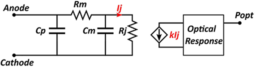
Figure 6. VCSEL equivalent circuit.
An essential set of measurement data was collected from procured samples through two main setups (DC and S-parameter) that quantified the static and dynamic characteristics of the device. The measurement setup for the DC response of the VCSEL is shown in Figure 7A, while the setup for S-parameter measurements is shown in Figure 7B. The VCSEL was probed on a chuck, which supported temperature control, this way enabling temperature sweeps. Current vs. optical power (I–P) and current vs. voltage (I–V) data were produced, as well as S21 and S11 parameters, which capture the variable bandwidth and input impedance characteristics, over different temperature and bias points. The relations derived from the experimental data were fitted to produce the corresponding model for each device. Measurement results along with the performance of the model are shown for DC in Figure 8A and S21 in Figure 8B.
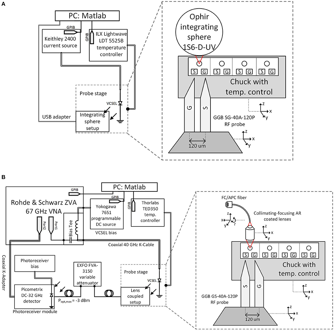
Figure 7. Characterization setups for the VCSEL. (A)Test bench for IPV measurements. (B) Test bench for S-parameter measurements.
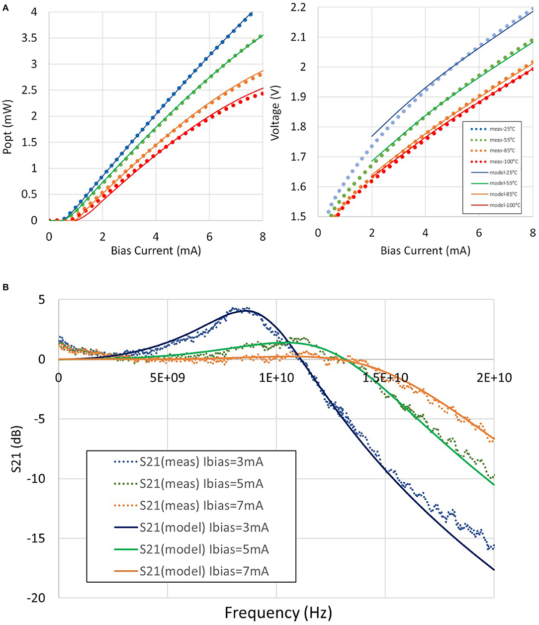
Figure 8. Comparison between measured (dotted lines) and modeled (solid lines) VCSEL parameters. (A) DC measurement vs. modeled results for different temperature settings. (B) Normalized S21 measurement vs. modeled results for different bias settings.
Vertical-Cavity Surface-Emitting Laser Driver Topology
The operational environment for the VCSEL driver poses a trade-off that stands out in the design process. This is between the desired robustness to handle space effects and power consumption. The reason is that the main design principles and techniques that are conventionally proposed [10], such as differential design, averaging, etc. are methodologies, which in most cases increase redundancy in the processing chain to alleviate the magnitude of the different effects, thus power consumption increases correspondingly.
A main goal for addressing this is to target the least-consuming operating mode for the VCSEL that would respect performance target. Referring to Figure 8B, meeting the requirement for a data rate around 25–28 Gb/s could be easily met from a bandwidth standpoint, with a bias current of 7 mA, which is actually the one proposed as nominal by the manufacturer. However, there indeed seems to be room to optimize performance by targeting a lower bias point even around 5 mA. Also, it is important to note that the benefit of a reduced operating current is 2-fold. Besides expected savings in power consumption, a low-current operation also leaves sufficient room for compensation during the aging process of the VCSEL.
The design for the 28 Gb/s VCSEL driver circuit was carried out with a focus on overall robustness, tunability, and energy efficiency. The VCSEL driver circuit was specified to integrate four channels with a total throughput of 112 Gb/s and power consumption of <100 mW per channel. To facilitate simple module regulation, a single supply of 3.3 V was decided.
The functional diagram of the driver is shown in Figure 9. The driver receives OOK data and may directly modulate the VCSEL with a programmable swing. The differential input is terminated on-chip with 100 Ω, and an internal reference provides the input common-mode voltage, permitting input AC coupling with the preceding stage to avoid DC loading. Considering the option of AC coupling for the output as well, the low-frequency components present, depending on the number of allowable consecutive identical bits and the code used, would require design modifications and coupling capacitors of impractical size for on-chip or in-module integration. Therefore, DC coupling has been selected for the driver output. The output provides signal and ground pins for connecting the VCSEL in a common cathode topology. This choice permits connection of the four channels of the driver directly with a × 4-VCSEL array developed on a common ground substrate.
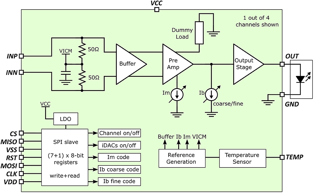
Figure 9. VCSEL driver block diagram.
The driver is designed in three stages: an input “buffer” stage, which receives the data, a “pre-amp” programmable stage, and a high-current “output stage.” The pre-amp stage features programmable modulation current (Im) and bias current (Ib), with coarse and fine tuning by employing three current DACs. The pre-amp stage is implemented as a differential amplifier, and the unused output is terminated with a low-consumption dummy load of equivalent impedance to the output stage. Finally, the output stage is a high-current switching one, which features channel shut-down capability.
The dedicated Reference Generation block provides reference currents for the buffer stage and the on-chip current DACs implementing the programmable features. It is attached to a temperature sensor to provide temperature-independent currents. The temperature sensor outputs a voltage proportional to temperature so as to monitor the temperature fluctuations within the die.
Programming of the output is implemented with an on-chip Serial Peripheral Interface (SPI) slave interface, which will be presented in a subsequent section. It features eight 8-bit registers, seven for control and one for diagnostics. Through the SPI, independent channel output activation and deactivation and programming of the output swing for every channel can be performed. The digital circuit is powered independently from a 1.2 V supply, which is provided by an on-chip low dropout regulator (LDO). The regulator reference is provided by a dedicated bandgap reference generation circuit. The register outputs are level-shifted to interface the analog core. The SPI interface output bus is connected to the current DAC inputs and gating transistors. Each channel is controlled by two 8-bit registers with four control bits for DAC and channel output activation, and three 4-bit words for current swing tuning. The digital interface features a reset function that initializes the circuit.
Physical Design and Performance
The VCSEL driver top layout view where the main areas of the chip are identified is shown in Figure 10. To assess performance, post-layout simulations were performed after parasitic extraction. The test bench includes pseudo-random binary sequence (PRBS) generation for input differential voltage swing, AC-coupling caps and models for module routing through the connector and interposer, and transmission lines (TL) to reach the extracted net list block for the driver input. Equivalently, the driver output is connected to the VCSEL model block through a transmission line model for output routing. The schematic of the test bench is shown in Figure 11A.
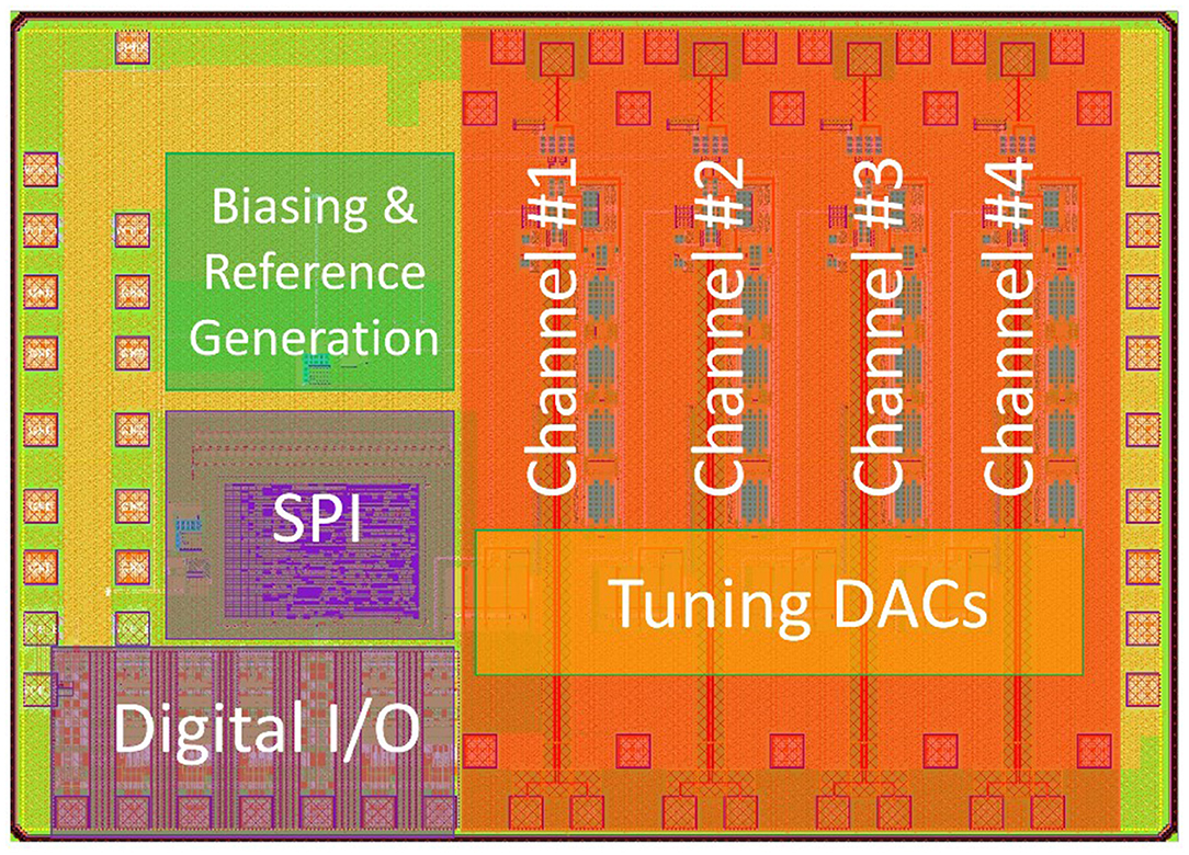
Figure 10. VCSEL driver top layout with block functions identified.
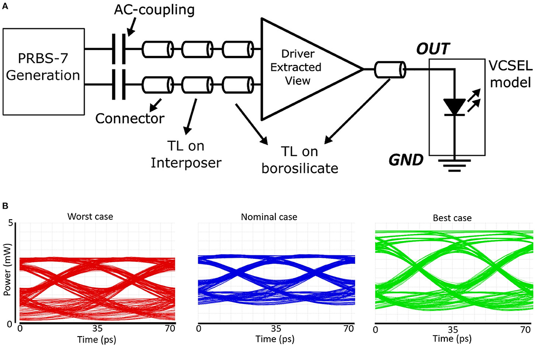
Figure 11. VCSEL driver test setup. (A) Schematic test bench for performance simulations that include EM models for routing. (B) Simulated worst, typical, and best-case eye diagrams for 28 Gb/s.
In Figure 11B, 28-Gb/s eye diagrams are presented for the scenarios detailed in Table 4. Motivated by pushing for the lowest power consumption within the link budget, a 3/7 mA swing was chosen as an affordable choice for relatively low temperatures (best case). However, at increased temperatures, the eye of this current setting might be challenged as bandwidth drops to borderline in meeting the required speed (worst case), so an increase in current might be required to 4/8 mA, which represents the nominal point of operation. At 25°C, power consumption is 74 mW per lane, which grants the driver an energy efficiency of 2.64 mW/Gb/s.
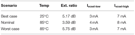
Table 4. Vertical-cavity surface-emitting laser driver design scenarios.
Transimpedance Amplifier IC Circuit
From System to Circuit: TIA Requirements
Prior to starting the TIA development, the design parameters and their range must be fixed. We determined the worst-case scenario as an operation at the highest temperature and having maximum losses within the channel. In this case, the TIA should demonstrate minimum noise performance and maximum gain. On the other hand, the best-case scenario implies operation at low temperature with low losses. In this case, the TIA must be able to process high input current. Correspondingly, the noise requirements are relaxed, and the transimpedance gain should be decreased to avoid saturating the circuit. A system-level analysis of the optical link (Section 1) results in TIA requirements, summarized in Table 5. It is assumed that each TIA channel should deliver 400 mVpp differentially into a 100-Ω load at a 28 Gb/s data rate.
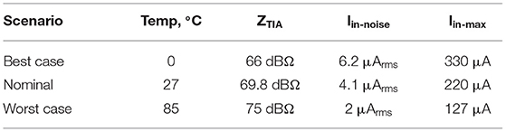
Table 5. Transimpedance amplifier design parameter range.
To cover the transimpedance range, shown above, controllability has to be implemented. Another design parameter that should have a possibility of external adjustment is a TIA output swing. It can be useful not only for compensating module losses but also losses in the signal path outside of the module.
If we consider the targeted power efficiency for a transceiver to be at 10 mW/Gb/s, assuming equal power distribution between both ICs, then the TIA/driver power consumption goal results in 140 mW per channel. One way to reduce the power consumption for high-speed circuits is operating at the lowest possible supply voltage while keeping the required eye-opening at a given data rate. Thus, another TIA design requirement will be reliable operation within a wide supply voltage range, which was set to be in the range of 2.5–3.3 V. Having all the TIA requirements determined, TIA circuit design can be conducted.
Transimpedance Amplifier Circuit Design
The four-channel TIA, as shown in Figure 12, consists of the following building blocks:
– TIA cores, each having a single-ended input and a differential output
– 16 digital-to-analog converters (DACs) to set the bias currents in the TIAs
– RH digital interface (SPI) to control the DACs
– low pass filter for photodetector (PD) biasing
– temperature sensor
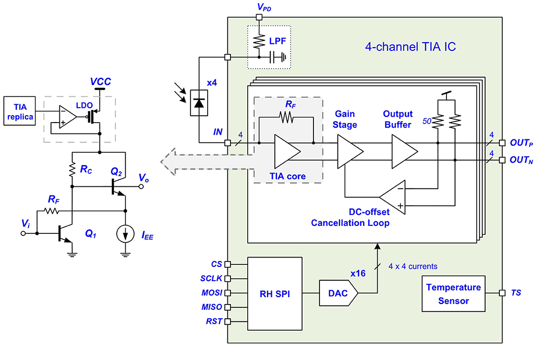
Figure 12. TIA IC block diagram and TIA core schematic.
As a TIA core, a common-emitter amplifier with resistive shunt feedback has been chosen (Figure 12). This architecture is well-known for its broadband response and good noise performance. However, it has a low power supply rejection ratio, which has to be considered in multichannel systems. Therefore, a separate low-dropout regulator (LDO) circuit was used for a TIA core in each channel. The LDO provides to the TIA core a supply voltage in the range of 2–2.4 V, depending on the current that is set in a TIA replica circuit and controlled through an SPI interface.
A gain stage represents a two-stage differential cascode amplifier. In both stages, inductive peaking was applied to achieve the required bandwidth. The output of the first stage receives a feedback signal from the TIA output for correcting a DC-offset, which might be because of the amplified DC mismatch between balanced TIA outputs. An output buffer is realized as a cascode differential pair with a load resistance of 50 Ω at each branch. This value minimizes TIA output reflection losses in the presence of onboard transmission line model. Each of the TIA channels receives four controlled currents generated by a four-channel DAC, allowing noise tuning, transimpedance, and output swing adjustments. There are four four-channel DACs on the ASIC. Each four-channel DAC has its separated bias reference network. Thus, in case of a particle strike on a single channel's biasing circuit, the operation of the other channels will not be affected.
Post-layout simulations were performed on the TIA circuit to include realistic effects.
Figure 13A shows TIA transimpedance gain plots over corner conditions. Similar to the system design, worst-case conditions reflect operation at the highest temperature (85°C) and use worst-case component models. A nominal case corresponds to the operation at room temperature, having nominal models for simulation. Similarly, Figure 13B presents the noise behavior of a TIA channel across different scenarios. An integrated input-referred noise within a 3-dB bandwidth is not higher than 2.5 μArms over all corner conditions. This satisfies the nominal and best-case system requirement presented in section From System to Circuit: TIA Requirements. However, a worst-case noise requirement could not be achieved. Nevertheless, the circuit was accepted for fabrication, because the probability of worst-case performance for all components within the optical link at the same time is very low.
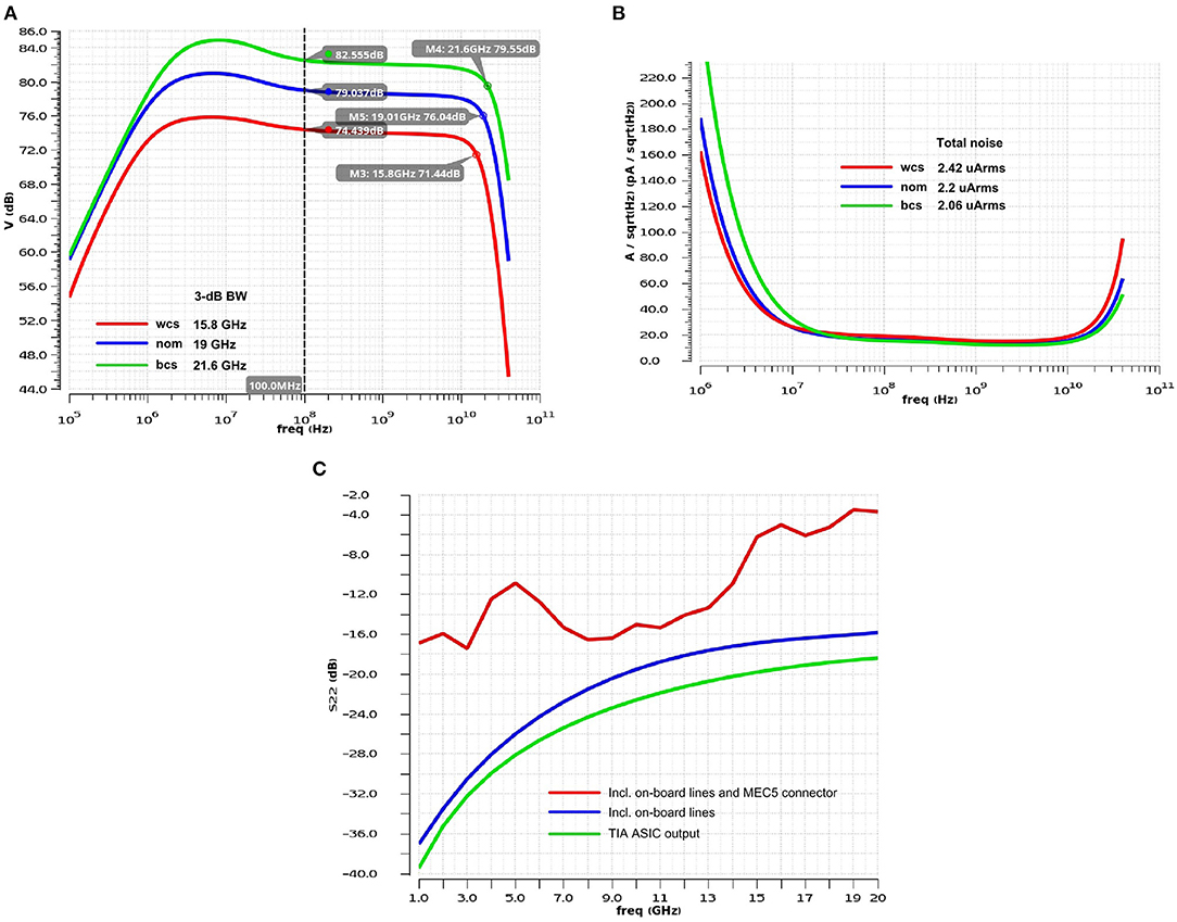
Figure 13. TIA metrics at default SPI register settings and at a 3-V supply voltage: (A) transimpedance gain; (B) input-referred noise current density; (C) TIA ASIC output reflection losses.
Figure 13C shows the TIA ASIC output reflection losses when the differential output is loaded by 100 Ω. The green curve shows an S22 parameter of the TIA at the ASIC pads. This corresponds to a case in which a TIA ASIC is going to be measured on-wafer, having the calibration plane at probe tips. The blue S22 curve includes the transmission lines on module substrate; and, finally, the red S22 curve shows the expected output return loss in the receiving part of the module at the output of a connector.
The post-layout TIA model, loaded by the module interconnect model with an on-board connector, was also analyzed in the time domain.
Figure 14 shows the corresponding eye diagrams of the complete chain for a 28 Gb/s data rate. The simulation was performed under different corner conditions. For the worst- and nominal cases, the TIA input receives a PD current of Idc/Ipp = 50/80 μA at 0 and 27°C; whereas for the best-case scenario, the input current is equal to Idc/Ipp = 130/200 μA, and the TIA circuit operates at 85°C. As the TIA circuit is biased at the middle current values, it is possible, depending on the real performance, to change the current settings in a way that the required output swing/eye opening can be adjusted.
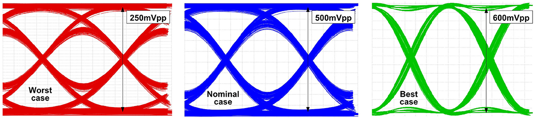
Figure 14. Differential eye diagrams at the module output including TIA post layout simulation.
Figure 15 shows a four-channel 112 Gb/s RH TIA ASIC layout. As can be seen in the figure, the output transmission lines are quite long compared with the active part of a TIA channel. The length of each line is equal to 900 μm. This is because the designed TIA has to fit into the pre-defined pad configuration. The total IC area is 2.6 mm2. For future designs, the layout can be optimized to have the output transmission lines ~400 μm shorter, which would result in an occupied area of below 2 mm2.
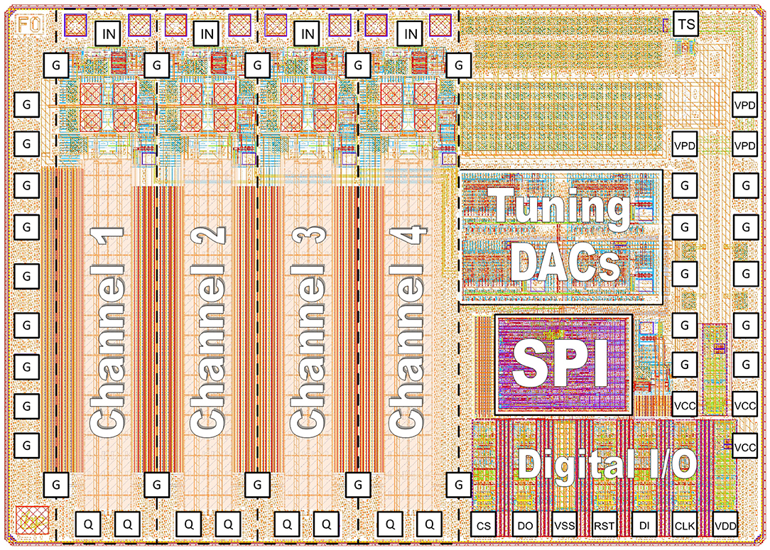
Figure 15. A four-channel TIA IC layout.
For the TIA circuit, the default values of the SPI are set in a way that all of the reference currents in the TIA circuit are a bit higher than half of the maximum current (9/16 of Imax). In this case, within the complete module, the complete four-channel TIA IC dissipates to 350 mW from a 3 V supply voltage, resulting in power consumption of 87.5 mW per channel or a 3.2 mW/Gb/s efficiency, which lets enough power efficiency margin for the VCSEL driver IC. Naturally, a stand-alone TIA IC with 100 Ω differential load only shows much better results in terms of power efficiency. Table 6 summarizes the post layout simulation results of a one channel TIA, that delivers a 400 mVpp differential signal to the load during a nominal case of operation.
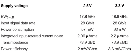
Table 6. One-channel TIA performance summary at different supply voltages.
As the TIA IC has widely controlled parameters within the 2.5–3.3 V supply voltage range, it will help, to some extent, to tolerate the imperfections in IC fabrication, module assembly, and changing environmental conditions.
SPI Slave
An on-chip SPI slave circuit has the possibility to set hardwired initial register values. This will simplify the characterization of the IC, since the functional test can be done without programming the SPI slave, which means that the SPI master may not be connected.
The SPI core was synthesized using the RH digital library that contains RH triple modular redundancy flip-flop cells and combinatorial logic. The SPI clock tree utilizes RH drivers. The RH SPI core occupies an area of 340 × 240 μm2, which is ~3.3 times bigger than the SPI core based on standard non-RH cells. A separate LDO circuit provides a supply voltage of 1.2 V for the SPI core from the external VDD pin, which might be set in a range from 2.5 to 3.3 V. Total power consumption of the SPI is below 2 mW during the operation. For operation in space, a relatively slow SPI clock signal should be continuously applied in order to prevent the register values from flipping.
Comparison With Literature
Compared with the state-of-the-art literature, the packaged 4 × 10 Gbps transceiver in Karppinen et al. [6] achieved 40 Gbps with an energy efficiency of 4.5 mW/Gbps per channel. The 2 × 3 × 25 Gbps integrated transmitters and receivers in Stampoulidis et al. [8] demonstrated a 17.5 Gbps error-free performance for a total of 107 Gbps and energy efficiency of 6.26 mW/Gbps when packaged on a demonstrator board. The proposed differential transceiver with fully integrated mid-board optics achieved an energy efficiency of <6 mW/Gb/s for the entire link at 112 Gb/s transmission which is the highest reported data rate from a single ASIC and, to the best knowledge of the authors, the first with pluggable mid-board optics featuring custom build RH ICs.
Conclusions
In this study, we report the design of a 112 Gb/s VCSEL-based optical transceiver aimed for application to intra-satellite optical interconnects. A top-down design approach was followed starting from module specification. The use of a borosilicate substrate for electrical and optical routing and flip-chip processing for all components enables high data rates in a small form factor. The challenges of the space environment, along with package and VCSEL measurements, and modeling were factored in the design and optimization of the transceiver chipset. Integrated SPI interfaces and IDAC references allow several degrees of control and programmability for both ICs. The 4 × 28 Gb/s Tx and Rx ASICs are designed in the IHP 130 nm SiGe BiCMOS process (SG13RH) leveraging proven robustness in radiation environments and high-speed performance featuring bipolar transistors (HBTs) with fT/fMAX values of up to 250/340 GHz. The designed ICs target to achieve energy efficiency of <2.65 mW/Gb/s for the Tx and <3.3 mW/Gb/s for the Rx from a 3.3 V supply for a total of <6 mW/Gb/s for the entire link.
Data Availability Statement
The original contributions presented in the study are included in the article/supplementary material, further inquiries can be directed to the corresponding author.
Author Contributions
PA, NV, AM, and MS contributed definitions of the system requirements in the Introduction section, performed simulations to enhance the main physical parameters, and established optical budget links. SG and IS designed the driver IC. SG also organized the measurement campaign for VCSEL characterization with support and direction from AG and HZ and undertook manuscript finalization and submission. LS contributed to system-level simulations. IS also contributed to the section about the VCSEL driver and compiled all manuscript contributions. GF managed this project for IHP. PO designed the TIA IC and wrote the corresponding section. FT performed radiation environment analysis summarized in the corresponding section. KT-H and GP designed the digital core used in both ASICs. IO managed this project for ALTER United Kingdom and contributed to package design. GW performed package design. SJ contributed the material to organize the section about the onboard optics module and also contributed to package design. All authors contributed to the article and approved the submitted version.
Funding
This study was conducted within the framework of the H2020-SPACE-SIPHODIAS project, and funding was received from the Horizon 2020 Research and Innovation Programme of the European Union under Grant Agreement No. 870522.
Conflict of Interest
IS and LS are part of Leo Space Photonics R&D. The research of SG has been funded in part by Leo Space Photonics R&D. AM, MS, and NV are employed by Thales Alenia Space. SJ, GW, and IO are employed by ALTER TECHNOLOGY TÜV NORD United Kingdom.
The remaining authors declare that the research was conducted in the absence of any commercial or financial relationships that could be construed as a potential conflict of interest.
Acknowledgments
The team at ALTER TECHNOLOGY TÜV NORD United Kingdom would like to thank Juan Barbero, Ainztane Lujambio Genua, and David Poudereux Sánchez from ALTER TECHNOLOGY TÜV NORD SAU for the ongoing assistance in screening component selection and their commitment to radiation and evaluation testing of the final assembled transceiver product.
Footnotes
1. ^Samtec MEC5-RA. Available online at: https://www.samtec.com/products/mec5-ra.
2. ^Consortium for On-Board Optics: Trends in Optical Networking Communications (White paper).
References
1. Venet N, Enjolras V, Nicolas C, Voisin P. Spaceflex onboard digital transparent processor: a new generation of DTP with optical digital interconnects. In: Proceedings of SPIE 11180, International Conference on Space Optics — ICSO 2018. Chania (2019). p. 111804B.
2. Blanchette G, Nezami MS, Rolston D, Reid B. Intra-satellite optical interconnect space market and technical challenges. In: Optical Interconnects XX, Vol. 11286. International Society for Optics and Photonics (2020). p. 1128604.
3. Westbergh P, Gustavsson JS, Haglund Å, Skold M, Joel A, Larsson. A. High-speed, low-current-density 850 nm VCSELs. IEEE J Selected Topics Quantum Electron. (2009) 15:694–703. doi: 10.1109/JSTQE.2009.2015465
4. Parkes S, McClements C, McLaren D, Florit AF, Villafranca AG. SpaceFibre: a multi-Gigabit/s interconnect for spacecraft onboard data handling. In: 2015 IEEE Aerospace Conference Big Sky, MT (2015). p. 1–13.
5. Karafolas N, Sodnik Z, Armengol JMP, Mckenzie I. Optical communications in space. In: 2009 International Conference on Optical Network Design and Modeling. Braunschweig (2009). p. 1–6.
6. Karppinen M, Tanskanen A, Ollila J, Heikkinen V. Fiber-optic transceivers for high-speed intra-satellite links. In: IEEE Avionics, Fiber-Optics and Photonics Digest CD. Cocoa Beach, FL (2012). p. 34–5.
7. Ko M, Tittelbach-Helmrich K, Petrovic V, Kissinger D. 25-Gb/s/Channel VCSEL driver and transimpedance amplifier array ICs in 0.25-μm SiGe:C BiCMOS technology for space applications. In: AMICSA 2016. Gothenburg (2016).
8. Stampoulidis L, Kehayas E, Karppinen M, Tanskanen A, Ollila J, Gustavsson J, et al. High-speed, low-power and board-mountable optical transceivers for scalable & energy efficient advanced on-board digital processors. In: Sodnick Z, Karafolas N, Cugny B, editors. International Conference on Space Optics-ICSO 2018. SPIE-The International Society for Optical Engineering. Bellingham (2018). p. UNSP 111804C.
9. Sourikopoulos L, Stampoulidis S, Giannakopoulos H, Zirath P, Ostrovskyy G, Fischer M, et al. The H2020-SPACE-SIPHODIAS project: space-grade opto-electronic interfaces for photonic digital and analogue very-high-throughput satellite payloads. In: International Conference on Space Optics—ICSO 2020. International Society for Optics and Photonics (2021).
10. ECSS-Q-HB-60-02A. Techniques for Radiation Effects Mitigation in ASICs and FPGAs Handbook ESA (2016). Available online at: https://ecss.nl/hbstms/ecss-q-hb-60-02a-techniques-for-radiation-effects-mitigation-in-asics-and-fpgas-handbook-1-september-2016-published/
11. SPENVIS. Space Environment Information System (SPENVIS) Version 4.6.10. European Space Agency (2021). Available online at: www.spenvis.oma.be
12. Evans H. Space environment basics & calculation methods. In: Radiation Environment and Its Effects in EEE Components and Hardness Assurance for Space Applications, CERN-ESA-SSC Workshop. Geneva: CERN (2016).
13. Lopez IG, Awny A, Rito P, Ko M, Ulusoy AC, Kissinger D. 100 Gb/s differential linear TIAs with less than 10 pA/Hz in 130-nm SiGe:C BiCMOS. IEEE J Solid State Circuits. (2018) 53:458–69. doi: 10.1109/JSSC.2017.2782080
14. Krstic M, Schmidt J, Breitenreiter A, Teply F, Sorge R. Evaluierung einer strahlungsharten Bibliothek in 0.13μm BiCMOS. In: Proceedings of DLR Bauteile Konferenz Ulm (2018).
15. Ostrovsky P, Schrape O, Tittelbach-Helmrich K, Herzel F, Fischer G, Hellmann D, et al. A radiation hardened 16 GS/s arbitrary waveform generator IC for a submillimeter wave chirp-transform spectrometer. In: Proceedings of IEEE Nordic Circuits and Systems Conference (NORCAS). Tallinn (2018). p. 1–4.
Keywords: very high throughput satellites, photonic payloads, optical interconnects, optical transceivers, VCSEL, photodiode, satellite communication
Citation: Giannakopoulos S, Sourikopoulos I, Stampoulidis L, Ostrovskyy P, Teply F, Tittelbach-Helmrich K, Panic G, Fischer G, Grabowski A, Zirath H, Ayzac P, Venet N, Maho A, Sotom M, Jones S, Wood G and Oxtoby I (2021) A 112 Gb/s Radiation-Hardened Mid-Board Optical Transceiver in 130-nm SiGe BiCMOS for Intra-Satellite Links. Front. Phys. 9:672941. doi: 10.3389/fphy.2021.672941
Received: 26 February 2021; Accepted: 20 April 2021;
Published: 17 May 2021.
Edited by:
Samit K. Ray, Indian Institute of Technology Kharagpur, IndiaReviewed by:
Junichi Fujikata, Photonics Electronics Technology Research Association, JapanKapil Debnath, Indian Institute of Technology Kharagpur, India
Copyright © 2021 Giannakopoulos, Sourikopoulos, Stampoulidis, Ostrovskyy, Teply, Tittelbach-Helmrich, Panic, Fischer, Grabowski, Zirath, Ayzac, Venet, Maho, Sotom, Jones, Wood and Oxtoby. This is an open-access article distributed under the terms of the Creative Commons Attribution License (CC BY). The use, distribution or reproduction in other forums is permitted, provided the original author(s) and the copyright owner(s) are credited and that the original publication in this journal is cited, in accordance with accepted academic practice. No use, distribution or reproduction is permitted which does not comply with these terms.
*Correspondence: Stavros Giannakopoulos, c3RhZ2lhQGNoYWxtZXJzLnNl