 Dan T. Nguyen
 Daniel A. Nolan
- Corning Inc., Corning, NY, United States
In this paper we present a novel conceptual method for all optical representation of binary numbers that could be used for all-optical binary logic components in optical digital computing, as well as for other applications. The new concept is based on effect of localization of light in specially designed binary photonics lattices whose central parts resemble the represented binaries, and the localizations occur due to breaking periodicities of the lattices. The proposed structures can be made with integrated photonics on-chip that are highly programmable and controllable. Most significantly, the working principle of the novel method doesn’t require nonlinear interaction between light and material, which is the most serious obstacle in the conventional method that uses optical transistors whose mechanism relies mainly on optical nonlinearity. We will discuss some technical challenges in developing the components.
Introduction
Moore’s Law predicts that the number of transistors on certain computer chips will double every 18 months, leading to a predicament in the modern era: traditional transistors are no longer able to keep up with current processing needs. Excessive heat slows down processor speeds due to their physical size limits, and metallic wires restrict the rate of signal transmission. Consequentially, doubling has already begun to falter due to the heat that is unavoidably generated from increasing the amounts of silicon circuitry compressed into small, finite spaces. Other fundamental challenges loom a few years away. Microprocessors currently have circuit features that are around 14 nm; by the early 2020s, they may reach 2–3 nm. At this small scale, electron behavior will be governed by quantum uncertainties that will make transistors hopelessly unreliable [1]. In light of these challenges, it is necessary to explore faster, more efficient technologies than classical electrical computing (EC) for future computing demands.
Optical computing (OC) possesses myriad advantages over current electrical computing (EC). Light does not have the same time response limitations of electronics, does not require insulators, and can even send hundreds or even thousands of photon signal streams simultaneously using different frequencies. Furthermore, optics allows for low-loss transmission and provides a large bandwidth; its multiplexing capability is well-suited for communicating several channels in parallel without interference. Photonics devices are compact, lightweight, inexpensive to manufacture, and better at storing information than magnetic materials. By replacing electrons and wires with photons and photonics structures, researchers have hoped to build a new generation of computers that work 100 million times faster than today’s machines. Conservatively, an optical computer could perform more than 1017 bits operations per second—a huge difference compared to the gigabits (109) or terabits (1012) per second rates which electronics are either currently limited to or hoping to achieve [2–5]. Thus, OC represents a massive improvement over the computing capabilities presently available.
In addition, OC may be closer to realization than quantum computing (QC) -- the only other computing technology known to be superior than current EC. However, quantum computers, including quantum simulators, are still in the relatively early stages of research. Most components of the future quantum computers have not been defined yet, and technologies will need time to develop these components once the prototypes are established. It is also unknown when they might become available and commercialized. More importantly, in principle, quantum computers would increase greatly (exponentially, for some problems) the efficiency of solving problems such as factoring large integers, combinatorial optimization, quantum physics, and quantum chemistry simulations. Many of those problems are classically intractable computing. However, quantum computers by design would be less efficient than classical counterparts in a vast majority of problems in science and technology [6, 7]. Meanwhile, over the past few decades, photonics technologies have achieved breakthroughs crucial for many important components of future optical computers. These include optical memory, optical logic gate, Si-waveguide nano-photonics structures, and more. Therefore, all-optical digital computers promise to perform computing operations at light speed in digital logic, which would revolutionize the field of information and communication with or without the successful developments of QC.
However, despite decades of effort and progress made in related technical fields, the goal of an all-optical computer has remained largely unfulfilled. One of the reasons for this shortcoming is that optics are not suitable for carrying out calculations–at least in binary “0s” and “1s” [3]. It is important to note that some key components of an all-optical digital computer, such as devices that can optically perform the representation of binary and arithmetic operations, have not been successful for computing. Among the most challenging tasks: developing integrated on-chip, all-optical binary representation components, and searching for materials of high optical nonlinearity to provide low energy optical switches that could overcome the processing bottleneck to all-optical-computing. Optical computing is mostly analogue while electronic computing is digital. Digital optical computers were not able to compete with electronic computers due to the lack of appropriate optical components [3, 4]. These components must especially be implementable for practical use in compact devices. On the other hand, photons do not interact with each other in free space whereas electrons interact strongly through their Coulomb repulsion. Therefore, photons (light) can only interact with each other in the presence of electrons in a material, and the strength of optically nonlinear interaction is much weaker than that of electrons. The consequence of that is very undesirable. The processing elements for an optical computer would require more power and larger dimensions than those for a conventional electronic computer using transistors. Optically nonlinear systems tend to be sensitive to imperfections and perturbations, and that would cause instabilities in operations [5, 8, 9]. Developing methods of overcoming these limitations represents the new Frontier of research in optical computing.
In this paper, we will present the results of our recent investigation that could be used to develop all-optical binary representation components for optical computing and other applications. The proposed structures can be made with integrated photonics on-chip that are highly programmable and controllable. Most important, the working principle of the proposed method doesn’t require nonlinear interaction between light and material, thus avoiding the most serious obstacle in the conventional method that uses optical transistors whose mechanism relies mainly on optical nonlinearity [5, 8–12]. Our proposed method of optical representation of binary (ORB) is based on effects of localization of light in binary photonics lattices (BPL) that will be presented in detail in this paper. The BPLs can be made with current technologies such as multicore fibers, laser-written waveguide arrays, and lithography etching Si-waveguides etc. As will be presented in this report, BPLs are designed with simple construction rules that resemble the binary numbers. The output localized distribution of photons (or powers) from BPLs can be used to represent binary numbers optically. Finally, we will point out some technical challenges in developing these components that can be used in real applications.
Our paper is organized as follows: Introduction. The construction of binary photonics lattices, and their uses for optical representation of binary numbers are presented in Binary Photonics Lattices for Binary Representation. Discussion and finally Conclusion.
Binary Photonics Lattices for Binary Representation
It is worth noting that the concept of binary photonics lattices originates from our previous works on quantum walks (QWs) in arrays of waveguides, especially the localization in quasi-periodic Fibonacci arrays of waveguides [13–15], and in our quasiperiodic Fibonacci multicore ring fiber (MCRF) [16]. The results from our previous works, in particular, the very good agreements between experiments and theoretical results on QWs [16], suggest that a photonics lattice composed with different waveguides that break periodicity of the normal lattices can create localizations of light in the system. Localization of light in arrays of waveguides have been investigated both with coherent [16–19] and quantum sources20 [20–23]. We have expanded our investigation to different structures, and among them, we found new structures—the binary photonics lattices (BPLs) that are simple but can be used for ORB that doesn’t require optical nonlinearity—–a long sought component for optical digital computing.
The Concept of Binary Photonics Lattices
In this subsection we describe how to construct the BPLs and its use for ORB. First, let’s assume generally that we can represent binary numbers by two optical elements (binary), especially by two different single-mode (SM) waveguides A and B (denoted by blue and orange solid circles in all figures, respectively). Furthermore, light confinement (localization) in waveguide (WG) A is stronger than in WG B, representing “1” and “0”, respectively, of the binary numbers. In our method of ORB, each number
Second, conventional binary representation (BR) of a decimal number is a series of digits “0” and “1s” with the unit digit being the rightmost one, and the higher orders of other digits are counted from the unit digit to the left. For example,
Third, note that the
As stated, we want to construct special
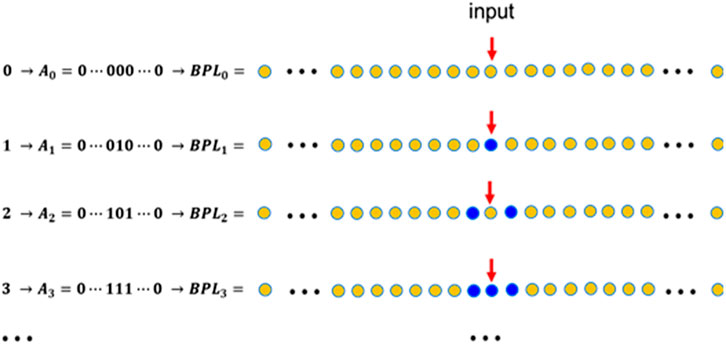
FIGURE 1. Schematic of
Table 1 above shows the mapping from a decimal number N to its general binary representation (binary from now on for short)
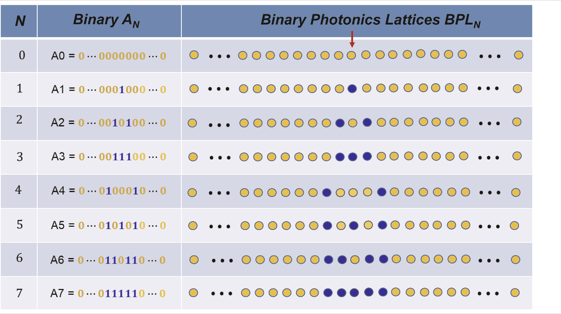
TABLE 1. Binary photonics lattices
Optical Representation of Binary by Binary Photonics Lattices
In this subsection, we will present our simulation results that show clearly the new BPLs can be used to perform an optically binary representation without optical nonlinearity as in the conventional method that uses optical transistors [5, 10–12]. It’s worth noting that our simulations are based on the beam propagation method (BPM) which is one of the most effective methods for simulating light propagation in complicated structures. The method of BPM has been first proposed by Feit and Fleck in the late 1970s [24, 25]. Since then, this method has been developed for vast applications and has been widely used in commercial software. We have developed our own MATLAB programs and successfully applied them to simulate complicated multimode cladding-pumped fiber amplifiers [26], and to design and optimize Yb-doped multicore fiber lasers in coherent Ising machines (CIM) [27, 28]. We have extended the method to simulate single photons QWs in periodic and quasiperiodic photonics lattices [13–15]. Furthermore, using the same approach, we have recently simulated and designed for fabrication of the first quasiperiodic Fibonacci MCRFs for realizing localized quantum walks (LQWs) [16]. Our simulation results are in very good agreement with experiments of quantum walks (QWs) and LQWs in periodic and quasiperiodic MCRFs, respectively, [16]. We will present the main concept of the simulation method in the Supplement. More details of this method can be found in [23, 24] and our previous publications [13–16, 26–28]. The simulation results of coherent light beam propagation in BPLs are presented in the following paragraphs.
We show in Figure 2 simulation results of light propagations in BPLs
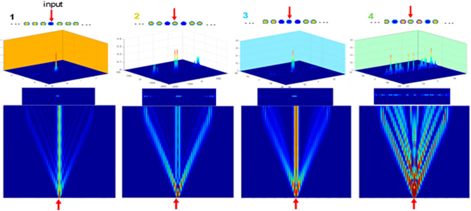
FIGURE 2. Light propagation in BPLs A1, A2, A3, and A4 (from left to right). Figures in the order from bottom to top: top-view, 2D front-view, 3D front-view of the output distributions of photons (power), and the binary photonics lattices are on top of each distribution. Red arrows indicate input signal λ=1.55 μm.
However, a closer look at the centers of these photon distributions in Figure 2 reveals some interesting patterns as shown in Figure 3.
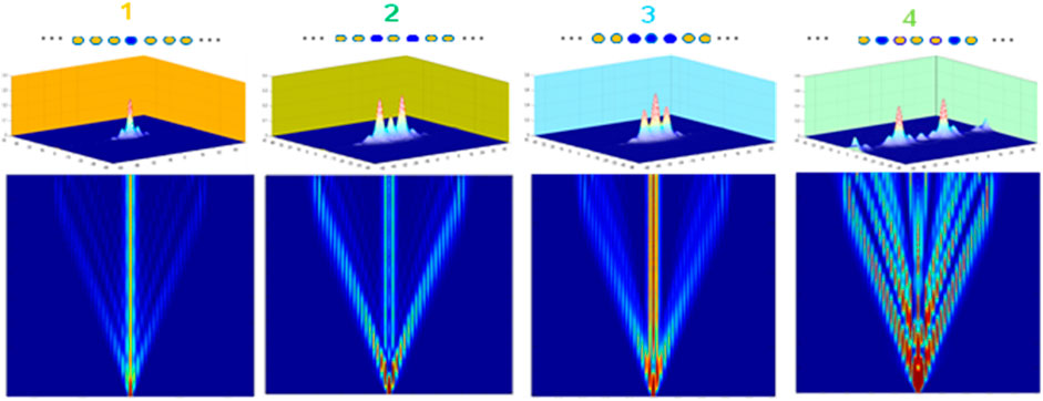
FIGURE 3. From the top to the bottom: center of BPLs from left to rightA1, A2, A3, and A4, center of photon distribution from these BPLs, top-view of light propagation in these BPLs. Centers of photon distribution from BPLs resemble the binary representation of corresponding numbers.
Figures 4, 5 below are the results for higher order BPLs A4 to A7, and all have 49 cores for presenting binary numbers from 4 to 7, respectively. Figure 4 shows the distributions of whole BPLs, meanwhile Figure 5 shows central parts of these distributions.
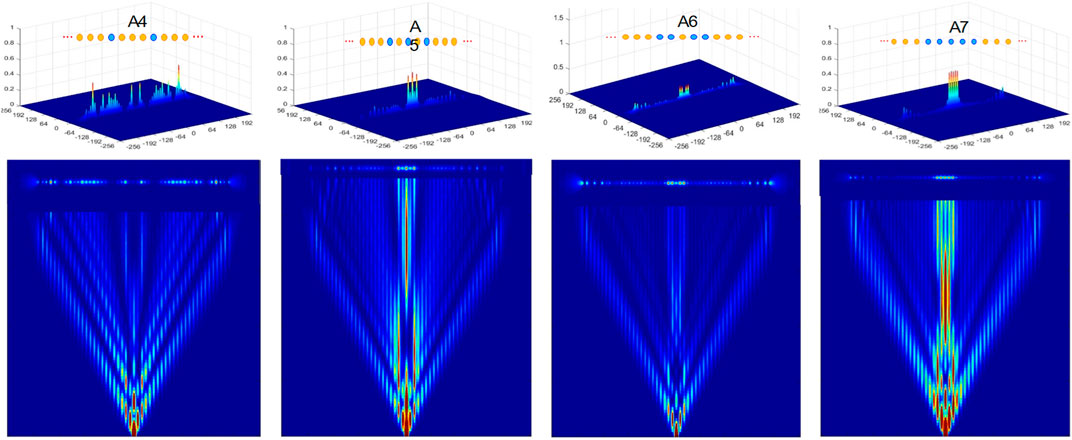
FIGURE 4. Light propagation in BPLs A4, A5 and A6, and A7, from the left to the right, respectively. Lower: top-view of light propagation, Middle: 2D front-view, and Upper: 3D front-view of the output photon distributions. Central cores of binary arrays of waveguides is on top of 3D output distribution.
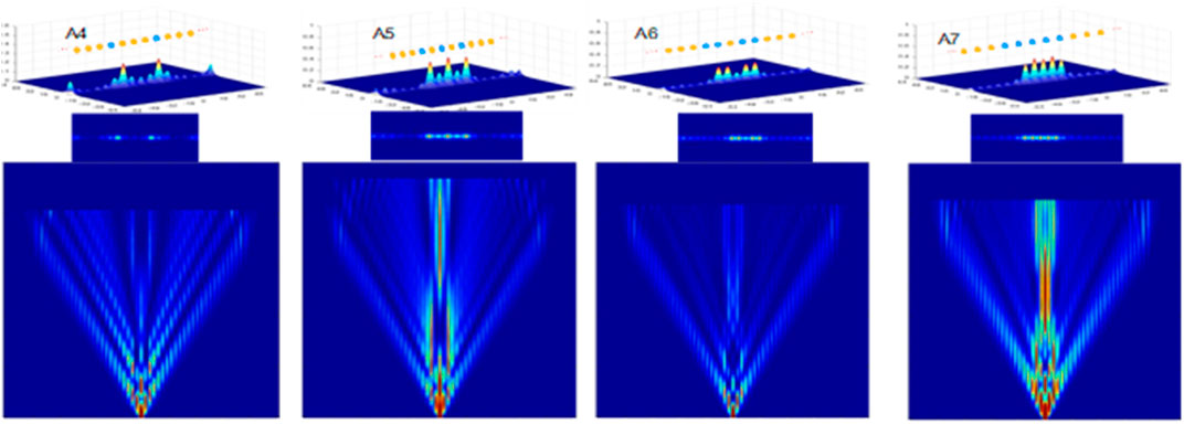
FIGURE 5. Light propagations in BPLs A4, A5, A6, and A7 similar to Figure 4, but only show center of distributions which clearly resembles the structures of central cores of corresponding BPLs.
In Figure 6 we compare distribution centers of BPLs A7 (left panel), A8 (center panel) and A10 (right panel) with the binaries 7, 8 and 10, respectively. The panels in Figure 6 are arranged from the bottom to the top in each panel as follows: the 3D-distribution of the whole lattice, the center of 3D-distribution (where binary number is represented), the center of 2D-distribution, the center of BPL and finally, the binary number.
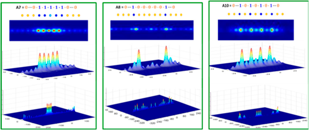
FIGURE 6. Center of distributions of BPLs A7(left panel), A8(central panel) and A10(right panel) resemble binaries 7, 8, and 10, respectively. See the text above for more details.
The results shown in Figures 3–6 are extraordinary in terms of the optical representation of binary: the BPLs can perform an optical representation of binaries without nonlinear interaction between light and material. Significantly, the working principle of the method doesn’t require optical nonlinearity, therefore avoiding one of the most challenging problems in developing optical digital computing, thus offering a feasible solution for long-sought components of optical digital computing. Furthermore, these BPLs structures can be made on-chip, integrated photonics devices that are essential for real application in optical computing.
Discussion
Our simulation results in previous sections show clearly that the localization of light in the photon distributions in binary photonics lattices (BPLs) can be used to represent binary numbers linearly, meaning that no nonlinear interaction between the light and material is required. The centers of photon distribution of BPLs resemble the corresponding binaries so beautifully. As shown in Figure 1 (and Table 1) the structures of BPLs look quite simple and straightforward to make. However, there are several important points in design and optimization that we would like to point out as follows.
First, it is easy to expect that the higher binary numbers, the higher numbers of cores in the BPLs. Our simulations show that the minimum number of BPL’s cores Nmin required for representing binary numbers are: 29 cores for representing binaries up to 22 = 4, 49 cores for binaries up to 23 = 8, and 69 cores for binaries up to 24 = 16, and so on. If that rule of scalability is held, we would need about 1,300 cores to represent all binaries up to 264 which is significant for applications. It is important to note that currently ultrafast lasers have been used to write waveguides in a photonics lattice of 49 × 49 = 2,401 waveguides [29].
Second, we would like to stress that although the principle of novel binary representation is quite simple, optimization for demonstration and applications would require a lot of effort.
For example, Figure 7 above shows the evolution of two BPLs A3 in 5 mm. The BPL A′3 on the left panel is the standard one with its definition in Table 1. In Figure 2, all WG As have the same index contrast ΔnA, and all WG Bs have the same index contrast ΔnB. In examples shown in Figure 7, the standard BPL A3 (left) ΔnA = 0.0045 and ΔnB = 0.0035. In the modified BPL A′3, all WG As have the same index contrast ΔnA = 0.0045 except for the center (input) core, which has a slightly lower ΔnA = 0.0042, indicated by a light blue color. All WG Bs have the same index contrast ΔnB = 0.0035 as in the standard one. In each panel, lower figures show distributions at two different distances indicated by two red lines. Note that the photon distribution in all A-cores of the modified BPL is more unformed than that in the standard one. The effect is predictable since the central A is also the input core and the light prefer to propagate in that input A rather than in the other WG As.
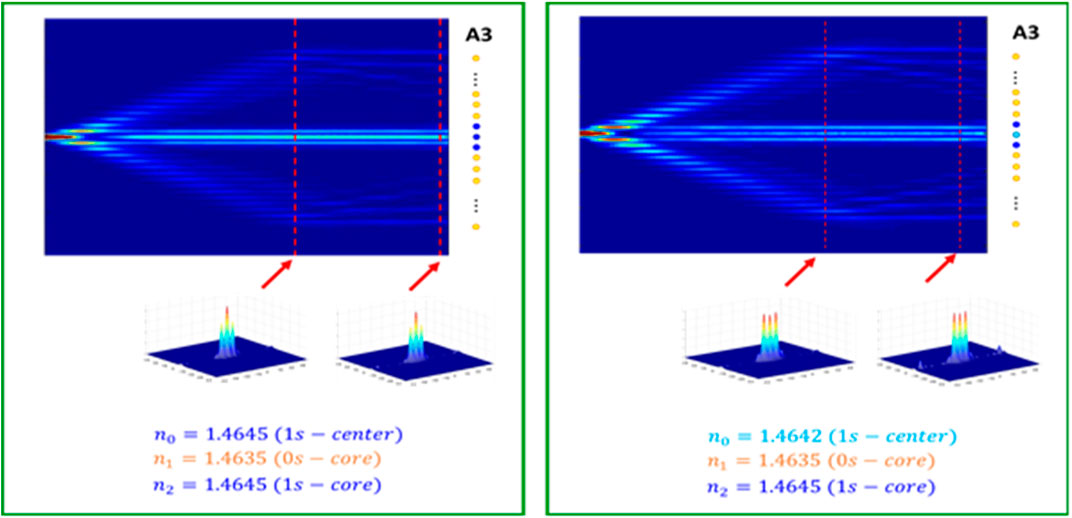
FIGURE 7. Light propagation in standard BPL A3 in 5 mm (left panel), and modified BPL A’3 (right panel). In the standard BPL, all cores As have same index contrast ΔnA, and all cores Bs have same index contrast ΔnB. In this example the standard BPL A3 (left) ΔnA = 0.0045 and ΔnB = 0.0035. In the modified BPL A’3, all cores As have same index contrast ΔnA = 0.0045 except for the center (input) core, which has lightly lower ΔnA = 0.0042, indicated by light blue color. All core Bs have same index contrast ΔnB = 0.0035 as in the standard one. In each panel, lower figures show distributions at two different distances indicated by two red lines. Note that, the distribution in modified BPL is more unformed than that in standard BPL.
Third, it is very important to point out that the binary representation of BPLs can be nearly preserved when the light propagates in one section of BPLs, as shown in the section between two red dotted lines in Figure 7. We will call it the binary presentation section–BPS. In real applications, we want to maximize BPS so that the measurements have a high tolerance along the length of the whole structure. Highly overlapping BPSs of all BPLs in applications are also preferable. Those will require a lot of optimization efforts.
Finally, we would like to discuss the effect of imperfection in the representation. We show in Figures 8, 9 the distributions of two BPLs A2 having 29 cores and 49 cores, respectively, with cores positions are 5% disorder displaced around regular places.
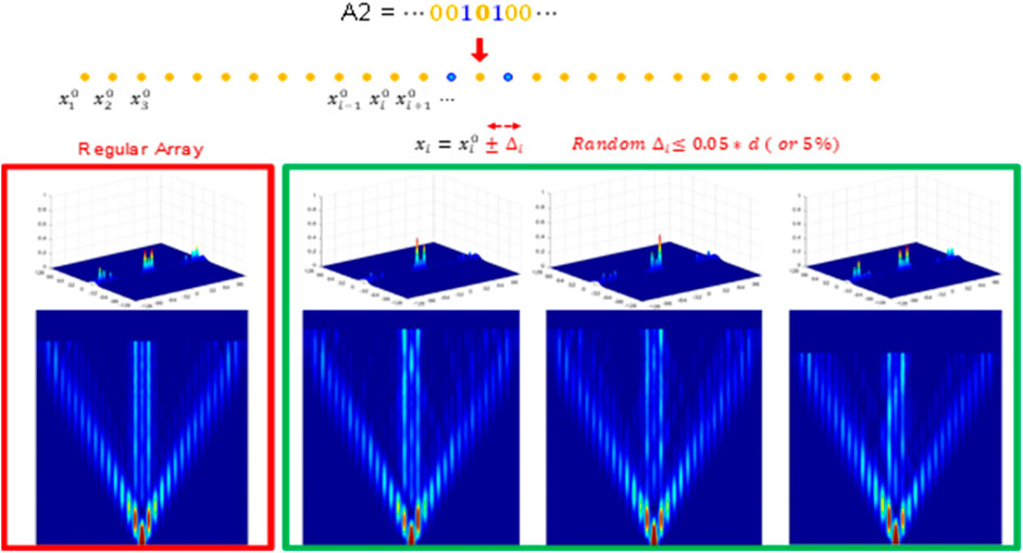
FIGURE 8. Light propagation and photon distribution in BPL A2 of 29 cores in which cores are placed 5% randomly disordered around their ideal, regular positions.
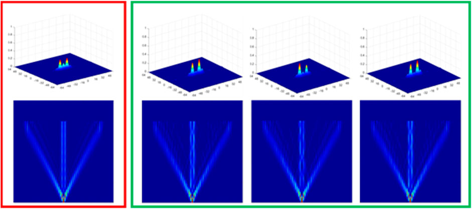
FIGURE 9. Light propagation in BPL A2 of 49 cores in which cores are placed 5% randomly disordered around their ideal, regular positions.
It is clear from Figures 8, 9 that the larger the core number, the cleaner the distribution at the center cores where we want to utilize for binary representation. The reason for that is there is an interference between the outside cores and the center ones. The larger the core numbers, the weaker the interference and cleaner the binary representation. Further investigation includes optimization to minimize the distortion with imperfection will be needed. The results in Figures 8, 9 also present challenges in manufacturing of binary lattices with large number of waveguides in which tolerances of only few percentages are acceptable for imperfections in variation of waveguides spacing, refractive indexes, diameters.
At this point, we would like to point out that all parameters used in our simulations are very normal ones in waveguide photonics or glass fibers. For example, the waveguides have the same core size of 4 μm, the center-to-center separation between the nearest cores is 8 μm, and the index difference between the core and cladding of WG B is Δn = 0.0035, and WG A is 0.0045. Therefore, fabrication of this structure doesn’t require very special materials and technologies. BPLs with numbers of cores from 50 to 70 are good enough to demonstrate the concept. However, for real applications, especially for digital optical computing, more than 1,300 cores would be needed.
Finally, we would like to stress that our proposed method using localization of light in special designed photonics lattices are for all optical representation of binaries. These structures that can be used for different applications, including optical computing, in incorporating with other components such as decoders, multipliers and/or logics gates, especially if these components are based on waveguides platform as investigated in Refs. [30–32].
Conclusion
In this work we proposed new binary photonics lattices (BPL) to perform optical representation of binary numbers. The BPLs are constructed symmetrically with two binary arrays of evanescently coupled waveguides. A beam of coherent light is launched into the central core and its propagation in the binary lattices can generate localizations of light in central parts that resemble the binaries we want to represent. Here, the light localizations occur due to the breaking periodicities of the lattices of two different SM waveguides, one represents 0, the other represent 1. Our simulations show the localizations in BPL’s photon distribution resemble binary structures, and therefore can be used to represent these binaries optically without the requirement of nonlinear interaction between light and material. Our results in this work can be considered as a conceptual method proposed for all optical represent of binaries. The proposed method is simpler to operate and control as compared with the conventional method using optical transistors that relied mainly on optical nonlinearity, which is one of the most challenging problems to be overcome in developing all-optical digital computing. Furthermore, the BPL structures can be made with integrated on-chip, that are highly programmable and controllable. Those are critical features for real applications.
Methods
In this work our modeling and simulations are based on beam propagation method (BPM), one of the most effective method for simulating light propagation [24, 25]. We have developed our own Matlab code of BPM for simulating the problem of single-photon quantum walks in arrays of waveguides or photonics lattices [13–15], which is the same for coherent light propagation in the lattices [16–21]. Our BPM simulations of single photon QWs or coherent light propagation have been validated experimentally in periodic and quasiperiodic multicore ring fibers (MCRFs) [16].
Data Availability Statement
The original contributions presented in the study are included in the article/supplementary material, further inquiries can be directed to the corresponding author.
Author Contributions
DTN proposed the idea of binary photonics lattices (BPL), performed the design and simulation. DAN and NFB helped develop the methodology and the applications of BPLs. All authors contributed to writing this paper.
Conflict of Interest
Authors DTN, DAN, and NFB were employed by the company Corning Inc.
Publisher’s Note
All claims expressed in this article are solely those of the authors and do not necessarily represent those of their affiliated organizations, or those of the publisher, the editors and the reviewers. Any product that may be evaluated in this article, or claim that may be made by its manufacturer, is not guaranteed or endorsed by the publisher.
Acknowledgments
The authors would like to thank Hannah Nguyen and Rita Cain for critical reading the manuscript.
References
3. Heck M. Optical Computers Light up the Horizon (2018). Available at: https://phys.org/news/2018-03-optical-horizon.html (Accessed March 20, 2018).
4. Ambs P. Optical Computing: A 60-Year Adventure. Adv Opt Tech (2010) 2010:1–15. doi:10.1155/2010/372652
5. Wherrett BS. Digital Optical Computing. In: A Miller, KR Welford, and B Daino, editors. “Nonlinear Optical Materials and Devices for Applications in Information Technology”, NATO ASI Series. Dordrecht, Boston and London: Kluwer Academic Publishers, 289 (1995).
6. Nielsen MA, Chuang IL. Quantum Computation and Quantum Information. New York: Cambridge University Press (2010). doi:10.1017/cbo9780511976667
7. Ladd TD, Jelezko F, Laflamme R, Nakamura Y, Monroe C, O’Brien JL. Quantum Computers. Nature (2010) 464:45–53. doi:10.1038/nature08812 |
9. Nguyen DT. Optical Instabilities and Chaos Due to the Virtual Formation of Biexcitons. Phys Lett (1994) A193:462–6.
11. Rajan R, Babu PR, Senthilnathan K. All-optical Logic gates Show Promise for Optical Computing. Photon Spectra (2018) 52:62–5.
12. Soljačić M, Ibanescu M, Luo C, Johnson SG, Fan S, Fink Y, et al. All-optical Switching Using Optical Bistability in Non-linear Photonic Crystals. In: A Adibi, A Scherer, and SY Lin, editors. Photonic Crystal Materials and Devices (San Jose: SPIE), 5000 (2003). 200–214.
13. Nguyen DT, Nolan DA, Borrelli NF (2019). Quantum Walks in Quasi-Periodic Arrays of Waveguides. Proc. SPIE 10933. In: Advances in Photonics of Quantum Computing, Memory, and Communication XII, San Jose, 109330X.
14. Nguyen DT, Nolan DA, Borrelli NF. Localized Quantum Walks in Quasi-Periodic Fibonacci Arrays of Waveguides. Opt Express (2019) 27:886–98. doi:10.1364/oe.27.000886 |
15. Nguyen DT, Nolan DA, Borrelli NF. Quantum Walks in Quasi-Periodic Photonics Lattices. In: Advances in Quantum Communication and Information. InTechOpen Publishing (2019).
16. Nguyen DT, Nguyen TA, Khrapko R, Nolan DA. Quantum Walks in Periodic and Quasiperiodic Fibonacci Fibers. Sci Rep (2020) 10:7156. doi:10.1038/s41598-020-64065-6 |
17. Martin L, Di Giuseppe G, Perez-Leija A, Keil R, Dreisow F, Heinrich M, et al. Anderson Localization in Optical Waveguide Arrays with off-diagonal Coupling Disorder. Opt Express (2011) 19:13636–46. doi:10.1364/oe.19.013636 |
18. Szameit A, Garanovich IL, Heinrich M, Sukhorukov AA, Dreisow F, Pertsch T, et al. Observation of Defect-Free Surface Modes in Optical Waveguide Arrays. Phys Rev Lett (2008) 101:203902. doi:10.1103/physrevlett.101.203902 |
19. Dreisow F, Szameit A, Heinrich M, Pertsch T, Nolte S, Tünnermann A, et al. Decay Control via Discrete-To-Continuum Coupling Modulation in an Optical Waveguide System. Phys Rev Lett (2008) 101:143602. doi:10.1103/physrevlett.101.143602 |
20. Thompson C, Vemuri C, Agarwal GS. Anderson Localization with Second Quantized fields in a Coupled Array of Waveguides. Phys Rev A (2010) 82:053805. doi:10.1103/physreva.82.053805
21. Perets HB, Lahini Y, Pozzi F, Sorel M, Morandotti R, Silberberg Y. Realization of Quantum Walks with Negligible Decoherence in Waveguide Lattices. Phys Rev Lett (2008) 100:170506. doi:10.1103/physrevlett.100.170506 |
22. Bromberg Y, Lahini Y, Morandotti YR, Silberberg Y. Quantum and Classical Correlations in Waveguide Lattices. Phys Rev Lett (2009) 102:253904. doi:10.1103/physrevlett.102.253904 |
23. Gräfe M, Heilmann R, Lebugle M, Silva DG, Leija AP, Szameit A. Integrated Photonic Quantum Walks. J Opt (2018) 18:103002.
24. Feit MD, Fleck JA. Light Propagation in Graded-index Optical Fibers. Appl Opt (1978) 17:3990–8. doi:10.1364/ao.17.003990 |
25. Feit MD, Fleck JA. Computation of Mode Properties in Optical Fiber Waveguides by a Propagating Beam Method. Appl Opt (1980) 19:1154. doi:10.1364/ao.19.001154 |
26. Nguyen DT, Chavez-Pirson A, Jiang S, Peyghambarian N. A Novel Approach of Modeling Cladding-Pumped Highly Er-Yb Co-Doped Fiber Amplifiers. IEEE J Quan Electron. (2007) 43:1018–27. doi:10.1109/jqe.2007.905010
27. Demir V, Akbulut M, Nguyen DT, Kaneda Y, Neifeld M, Peyghambarian N. Injection-locked, Single Frequency, Multi-Core Yb-Doped Phosphate Fiber Laser. Sci Rep (2019) 9:356. doi:10.1038/s41598-018-36687-4 |
28. Babaeian M, Nguyen DT, Demir V, Akbulut M, Blanche P-A, Kaneda Y, et al. A Single Shot Coherent Ising Machine Based on a Network of Injection-Locked Multicore Fiber Lasers. Nat Commun (2019) 10:3516. doi:10.1038/s41467-019-11548-4 |
29. Tang H, Lin X-F, Feng Z, Chen J-Y, Gao J, Sun K, et al. Experimental Two-Dimensional Quantum Walk on a Photonic Chip. Sci Adv (2018) 4:eaat3174. doi:10.1126/sciadv.aat3174 |
30. Kumar S, Bisht A, Singh G, Amphawan A. Implementation of 2-bit Multiplier Based on Electro-Optic Effect in Mach-Zehnder Interferometers. Opt Quant Electron (2015) 47:3667–88. doi:10.1007/s11082-015-0249-4
31. Kumar S, Bisht A, Singh G, Amphawan A. An Optical Synchronous up Counter Based on Electro-Optic Effect of Lithium Niobate Based Mach-Zehnder Interferometers. Opt Quant Electron (2015) 47:3613–26. doi:10.1007/s11082-015-0234-y
Keywords: localization of light, all optical representation of binaries, photonics lattices, arrays of waveguides, optical digital computing
Citation: Nguyen DT, Nolan DA and Borrelli NF (2021) Localization of Light in Photonics Lattices for All-Optical Representation of Binaries. Front. Phys. 9:709428. doi: 10.3389/fphy.2021.709428
Received: 13 May 2021; Accepted: 19 July 2021;
Published: 18 August 2021.
Edited by:
Venugopal Rao Soma, University of Hyderabad, IndiaReviewed by:
Ashok Vudayagiri, University of Hyderabad, IndiaSantosh Kumar, Liaocheng University, China
Copyright © 2021 Nguyen, Nolan and Borrelli. This is an open-access article distributed under the terms of the Creative Commons Attribution License (CC BY). The use, distribution or reproduction in other forums is permitted, provided the original author(s) and the copyright owner(s) are credited and that the original publication in this journal is cited, in accordance with accepted academic practice. No use, distribution or reproduction is permitted which does not comply with these terms.
*Correspondence: Dan T. Nguyen, bmd1eWVuZHQyQGNvcm5pbmcuY29t