 Cristina C. Gheorghiu
 Stefania C. Ionescu
 Petru Ghenuche
 Mihail O. Cernaianu
 Domenico Doria
 Daniel Popa
 Victor Leca*
- Extreme Light Infrastructure-Nuclear Physics (ELI-NP), Horia Hulubei National Institute for Physics and Nuclear Engineering (IFIN-HH), Magurele, Romania
The recent development of petawatt-class laser systems sets a focus on the development of ultra-thin free-standing targets to access enhanced particle acceleration schemes vital for future applications, such as, medical and laser-driven nuclear physics. Specific strategies are required to improve the laser-to-particle energy conversion efficiency and increase the maximum particle energy. One of the promising approaches is based on the target design optimization; either by tuning key parameters which will strongly affect the laser-matter interaction process (e.g., material, composition, density, thickness, lateral dimensions, and shape) or by using micro/nanostructures on the target surface. At ELI-NP, considerable efforts are dedicated to extend the target capabilities beyond simple planar target design and develop complex targets with tailored properties suitable for high-power laser-plasma interaction experiments, as well as for studies with gamma and positrons beams. The paper provides an overview of the manufacturing capabilities currently available within ELI-NP Targets Laboratory for providing users with certain types of solid targets, specifically micro/nanostructured gold and copper foils and microns thick, porous anodized alumina. Also, optimization studies of alternative patterns (micro/nanodots) on silicon substrate are presented for future implementation on metallic free-standing thin foils.
Introduction
As an integrated part of the ELI-NP facility, Target Laboratory provides the means for local fabrication, characterization, and microassembly of a broad range of solid targets. To ensure a successful experimental campaign, support throughout the process is ensured by the Target Laboratory team, from proposal evaluation of the target to technical feasibility and up to target delivery. Therefore, having an on-site Target Laboratory brings major benefits, e.g., avoiding the damage of fragile targets that usually occur during their transportation, meeting specific target requirements in terms of chemical stability and purity, and ongoing optimization of target key parameters. Also, custom-made possibilities and last-moment modifications and adjustments of the targets can be rapidly performed, using the feedback from the laser-matter interaction experiments. Thorough characterization of targets just before the shot can be locally provided, including for commercial targets, in the case additional data are required for the running experiments. Also, in the long run, additional reduced manufacturing costs due to internally developed technologies and methodologies, leading to competitive costs when compared with targets purchased from similar laboratories, are among other advantages. Depending on the complexity of the target, the fabrication process may take from few days (for supported thin films, multilayered samples) up to few months (for nanostructured, ultra-thin free-standing targets). Due to the large sample areas accepted by the existing (on-site) equipment used in the manufacturing and characterization steps (up to 6 inch in diameter), a relatively large number of solid targets can be obtained in a single process.
For the ongoing commissioning experiments at ELI-NP with the 1 PW laser [1], planar targets are provided either as commercial ones (e.g., thin/thick plastic films and metallic foils) or prepared in our laboratory (e.g., thin/ultra-thin films deposited on a template or as self-supported). One example of such planar targets that have been prepared on-site is the multilayer targets made of a controlled ratio of Fe-C homogeneous film. These targets can be employed to produce laser-driven secondary radiation which can be used in radiobiological and space radiation studies [2, 3]. Moreover, thin free-standing plastic targets (CH targets) are handled in-house, with the main focus on films of tens of nanometres in thickness and a few millimetres in the lateral dimension. In addition, special attention is given to the surface quality of planar targets (e.g., Al, Au, and Cu foils), which can impact laser absorption and particle acceleration. They can be improved by means of several in-house techniques, such as cold-rolling, electropolishing, mechanical polishing, thermal treatments, and dry or wet etching processes. Current continuous R&D activities of the manufacturing processes are directed towards providing the users with free-standing micro/nanostructured targets, by patterning the front and the backside of the targets with gratings, microspheres, micro/nanoparticles, hemi-spherical, or porous materials [4–11]. For these free-standing patterned targets, multiple-step fabrication procedures are currently tested and implemented by combining different manufacturing techniques with additional precise microassembling and mounting processes. Moreover, special attention is given to their quality, reproducibility, and optimization of the manufacturing process parameters.
For proton and ion acceleration experiments, we aim to take advantage of the unique opportunities provided by the high-power laser system at ELI-NP (high repetition rate and multi-petawatt power) [12–15], in order to obtain ion beams with large particle flux and with energy distribution suitable for the envisaged studies. As the characteristics of the laser-driven ion beams substantially depend on the target composition and configuration, several strategies intrinsically include the development of complex, more advanced targets. For example, the front side of the foil can be grooved as a diffraction grating or patterned as coupled plasmonic nanostructures, to confine and enhance the local optical field around these nanopatterns, thus allowing the optimization of light-matter interaction at sub-wavelength scale. An additional strategy includes the use of free-standing ordered porous arrays, which can also be used as a template for growing aligned metallic nanowires on an ultra-thin high-Z substrate (tens to hundreds of nanometres thick), foreseen to obtain high-Z and high-fluence accelerated ions for nuclear physics studies [16].
Although solid targets are intensively used in laser-plasma experiments, they exhibit some important limitations, as for instance, the need for a precise alignment before each shot, reducing the repetition rate of the shots; a poor resistance to the laser pre-pulse, that may lead to their destruction before the arrival of the main pulse, making the laser temporal contrast a critical factor. Moreover, thin and ultra-thin targets usually need to be grown on a substrate, then afterward requiring the removal of the support material [17, 18], that may be difficult and impact on the final quality. Another limitation, compared, for example, to gaseous targets, may be the difficulty in achieving mass production methods while keeping a good reproducibility; and that a significant amount of debris can be ejected during the laser-target interaction, which can severely damage the nearby optical elements. Using microelements on the front side of the target [19] provides strong coupling between the target and the laser by generating an intense electromagnetic field around their surface that can manipulate the electron dynamics, while structuring the backside gives mainly control on the ion beam geometrical characteristics [9, 11, 20, 21]. The energy absorption of the laser pulse is significantly enhanced depending on the shape and size of the microstructure; the laser-to-ion energy conversion efficiency is considerably increased [5, 22], leading to higher particle energy and flux. In this work, we give an overview of the manufacturing processes developed and currently available within ELI-NP Targets Laboratory for structuring free-standing metallic foils with nano- or microstructures as potential targets for the upcoming high-power laser experiments. For this, conventional structures have been chosen based on their correlation with future intended experimental campaigns, implementing and optimizing their manufacturing procedure on thin self-supporting metallic foils. Fabrication of porous alumina as prospective targets for laser-driven ion acceleration or as a template for metallic nanowires is also presented.
Materials and Methods
The micro- and nanostructured targets described in the present article have been obtained using the on-site fabrication and characterization capabilities available within the ELI-NP Target Laboratory, in an ISO 7 clean room environment [23]. Specifically, micro- and nanostructuring processes have been performed using an electron beam lithography system (DrawBeam EBL, Tescan) with proximity effect correction, implemented in the scanning electron microscope system. For the EBL process, 25–30 kV voltage has been used, while the specific process parameters are described in each target section. Reactive ion etching technique (RIE PlasmaPro Estrelas 100, Oxford Instruments Plasma Technology) for anisotropic dry etching processes by means of reactive plasma using a high-frequency (HF) generator, at 100–300 W, or inductively coupled plasma (ICP) unit, at 500–2500 W. The electrochemical setup used for aluminium anodization included a water-cooled double-jacketed electrochemical cell with a two-electrode system, a DC power supply (PSU 400–3.8, Gw Instek), and 2 bench-top multimeters (Peaktech 4075 and Keithley DMM6500) for current and voltage monitoring connected to a PC interface.
Sample surface analyses, performed in different stages of the fabrication process, have been achieved using the atomic force microscopy technique (AFM NTEGRA, NT-MDT), with a whisker-type carbon tip (11.5 N/m force constant, 255 kHz resonant frequency, 10 nm tip curvature radius, and 1 μm tip length); an optical microscope (Nikon, bright or dark field modes); an optical profilometer (S Neox, Sensofar) using confocal imaging, profiling, and interferometric measurements; and scanning electron microscopy (SEM MAIA3, Tescan) with an electron backscatter diffraction system (EBSD e-Flash 1000, Bruker), for crystal orientation and grain-size distribution analysis, and energy-dispersive X-ray spectroscopy (EDS X-Flash, Bruker), for elemental analysis of the samples. Where applicable, surface cleaning of the self-supported foils was performed prior to their use by Ar+ ion-milling with a Kaufmann ion source (KDC160 model), integrated into an ultra-high vacuum sputter deposition system (UHV deposition cluster, Mantis Deposition). Lapping and polishing of the surface of the samples was carried out using diamond abrasive slurries on a compact M.M.8400 machine (LamPlan), equipped with an automatic dosing unit (M.M.709) and ceramic conditioning rings, while colloidal silica was used for super-polishing processes. Annealing treatments of the samples were conducted in a muffle furnace (L9/13/P330, Nabertherm GmbH) for thermal treatments under a controlled atmosphere up to 1,300°C.
The free-standing foils used as supports for micro- and nanopatterning were 3 μm or 10 μm thick commercial Au and Cu foils of 99.9% purity and 25 × 25 mm2 size (Goodfellow). Al foils of 99.999% purity, 1 mm thick, and 150 × 150 mm2 size (Goodfellow) were used in the anodization experiments as raw material to attain free-standing anodic alumina films. Si wafers were used for preliminary tests on micro/nanodots and rods for process optimization and tuning key parameters before process transfer to metallic foils.
Micro/Nanostructured Targets Strategies
Metallic Gratings
To improve the laser-induced electron acceleration performances [24–26], the fabrication of patterned targets with ordered periodic gratings has also been considered. Such “grating” targets can be used for better control of the interaction of the ultra-intense laser pulse with matter via relativistic surface plasmons [25]. Compared to the previously reported studies, the approach presented in this paper is focused on the fabrication of gratings on thin free-standing metallic foils. Specifically, gold and copper foils have been patterned with periodic, one micron-size grating of rectangular or sinusoidal shape. A particular emphasis has been given to processes optimization, and several issues have been addressed, like handling difficulties, as the non-supported foils are easily bending, which was resolved by temporary fixing the self-supporting foil onto a one-inch Si wafer, providing better resistance to the foil and facilitating their handling. Additional issues involved the need for foils pre-processing before the patterning process, including cold-rolling and dry cleaning by controlled physical bombardment with Ar ions (i.e., Ar-ion milling). After the pre-processing of the foils, the gratings were fabricated using electron beam lithography and dry etching by Ar-ion milling. A schematic description of the fabrication procedure is depicted in Figure 1 and will be presented in detail elsewhere [27].
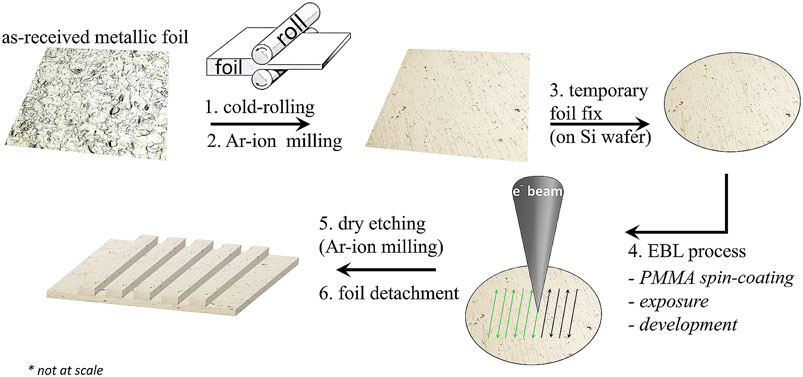
FIGURE 1. Scheme of the patterning procedure with microgratings on metallic foils (Au or Cu) (representation not at scale).
The flatness and roughness of the foils were found to be critical factors for fabricating high-quality gratings. These foils’ characteristics were significantly improved after a cold rolling process of the as-received foils, coupled with controlled Ar-ion milling. As shown in Figure 2 for an Au foil, a notable reduction of the roughness was achieved, from 350 nm of the original foil down to 13 nm. This process along with surface plasma cleaning operation on both sides was not detrimental and did not alter the average grain size, although a recrystallization process takes place at the surface of the foils. Experimental tests and theoretical simulations (using Monte Carlo simulations) allowed us to properly identify the following: (1) optimum exposure parameters for the EBL process (e.g., accelerating voltage, exposure dose, and step size) for 450 × 450 μm2 write field; (2) adequate developing conditions, e.g., developing time, developer dilution, and temperature; (3) appropriate resist removal technique, among the different physical and chemical methods, and their effects on the quality of the gratings; (4) suitable etching key parameters (e.g., gas flow, rotation speed, time, source power, cooling time, temperature, and angle). The exposure of the 600 nm-thick positive PMMA photoresist spin coated on the Au or Cu foils was done using an electron beam acceleration voltage of 30 keV, exposure dosage of 300 μC/cm2, and beam step size of 30 nm for a beam radius of 18.5 nm. For the development, resist removal, and etching processes, a mixture of 1:3 MIBK/IPA was used, for 120 s, followed by immersion in 1:9 MIBK/IPA solution for 30 s, at room temperature. Among different physical and chemical methods investigated to completely remove the hardened resist, while maintaining the quality of the structures, Ar-ion milling process (450 V and 100 mA, for 30 min) was found to be the most efficient. All Ar-ion milling steps were done at a pressure of 2 × 10⁻⁴ mbar Ar, with 7 rpm sample rotation, under room temperature. An angle of 45° between plasma direction and sample normal was used for yielding gratings with sinusoidal shape, and with normal incidence of the plasma to the sample surface, for rectangular shape gratings. A detailed description of the entire fabrication process is given in Ref. [27].
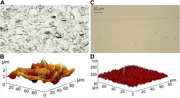
FIGURE 2. (A,C) Optical images, and (B,D) AFM 3D images of the Au foils: (A,B) as-received, and (C,D) after cold rolling and Ar-ion milling.
In Figure 3, the SEM images of metallic gratings patterned on 10 μm-thick Cu and Au free-standing foils (Figures 3A,B) and the gratings etched in 100 nm-thick Au layer deposited on Si substrate (Figure 3C) are illustrated. As can be observed, the quality of the gratings and the edges of the grooves are significantly improved in the case of the Au layer on backing support, indicating a more controlled and stable process due to the beneficial effect of the better-defined surface of the substrate.
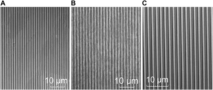
FIGURE 3. SEM images of metallic gratings with 1 μm-wide and ∼250 nm-deep groove etched on free-standing (A) Cu, (B) Au foils, and (C) on Au layer deposited on Si substrate.
Figure 4 shows the different profile shapes of gratings made on self-supported metallic foils, showing the two investigated types: rectangular and sinusoidal. The different geometries of the patterns have been achieved by varying the etching angle between the sample surface and the plasma direction. The rectangular profile, characterized by vertical walls, has been obtained using a perpendicular direction of the Ar ions to the surface of the sample. For the sinusoidal (namely, trapezoidal) profile, a 45° angle of incidence with respect to the sample surface was used, leading to this type of gratings profile due to the shadowing effect of the photoresist.
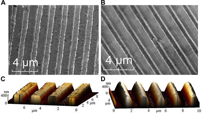
FIGURE 4. (A,B) SEM micrographs and (C,D) AFM 3D-images of 1 μm-wide Au and Cu gratings, with (A,C) rectangular and (B,D) sinusoidal shapes.
The patterned foils have been mounted on custom-made aluminium (Al) holders, whose design allows for 9 individual areas, e.g., targets (see Figure 5), increasing considerably the number of shots available in a single vacuum cycle of the interaction chamber. In experiments where full angular monitoring of the interaction is required (e.g., spatial distribution investigation of the high-energy particle beams and the characterization of the emission from the rear side of the target), the micrograting areas have been individually mounted on a thin capillary. Preliminary testing experiments of the structured foils, which will be presented elsewhere [27], showed that the electron beams emitted by the grating targets had up to 4 times higher flux than the flat foil. For the energy absorption, the grating targets were found to absorb 40% more of the laser energy than the flat foils, for a small laser incidence angle (<30°); for higher incidence angles, similar absorption was measured.
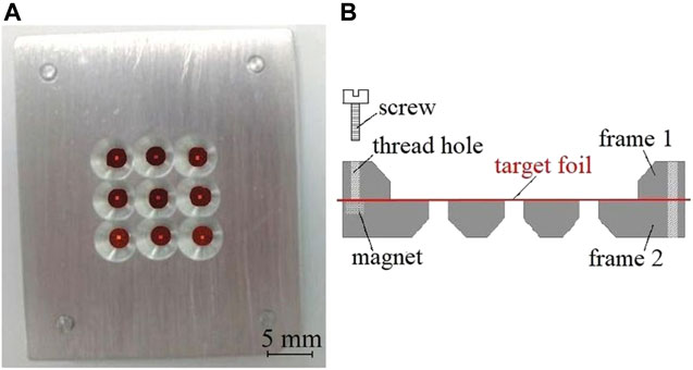
FIGURE 5. Al holder with patterned Cu foil for assembly demonstration purposes: (A) front side and (B) cross-sectional view.
Free-Standing Porous Alumina
Experimental studies on laser-driven particle acceleration, including particle-in-cell simulation, have been previously reported on aligned nanowires, with sub-wavelength dimensions [28–33], which are similar in structure to the anodic aluminium oxide template (AAO). One of the approaches used to improve the laser absorption in the laser-driven ion acceleration experiments is the nanostructuring of the substrates in a brush-like geometry to obtain nanometre-sized rods standing in an upright position [31]. These structures have the advantage of increasing the hot electron density and temperature that in turn can lead to enhancement ratios of 2–3 for the maximum proton energy. By controlling the porosity and thickness of similar structures made of free-standing porous alumina targets, we propose to investigate the improvement of the energy of the accelerated ions at intensities beyond 1021 W/cm2.
To obtain free-standing porous alumina (Figure 6), an Al foil of 20 × 50 × 1mm3 was annealed at 500°C for few hours to enhance the grain size in the metal [34], followed by mechanical polishing and then electropolished in a perchloric acid/ethanol mixture to improve the surface roughness (from 700 to 100 nm as the optical profilometer analysis has showed) and to lower the surface contaminants. The subsequent procedures included the two-step anodization in oxalic acid at 40V, 15°C, which transforms Al into aluminium oxide, resulting in a long-range honeycomb-like porous structure [35, 36]. After the first anodization, AAO was dissolved in a chromic/phosphoric acid mixture to eliminate the irregular template formed at the bottom [37]. The second anodization was performed under the same conditions, using an appropriate anodization time corresponding to the desired AAO thickness. For the free-standing AAO, a detachment method from the Al substrate was used by applying stair-like reverse biases in the same electrolyte used for anodization, usually from 18V to 24 V for 10 min each stair [38]. The bottom of AAO can be opened using a basic (NaOH 2M) or acidic (H3PO4 0.5M) solution to obtain open pores at both sides of the template.
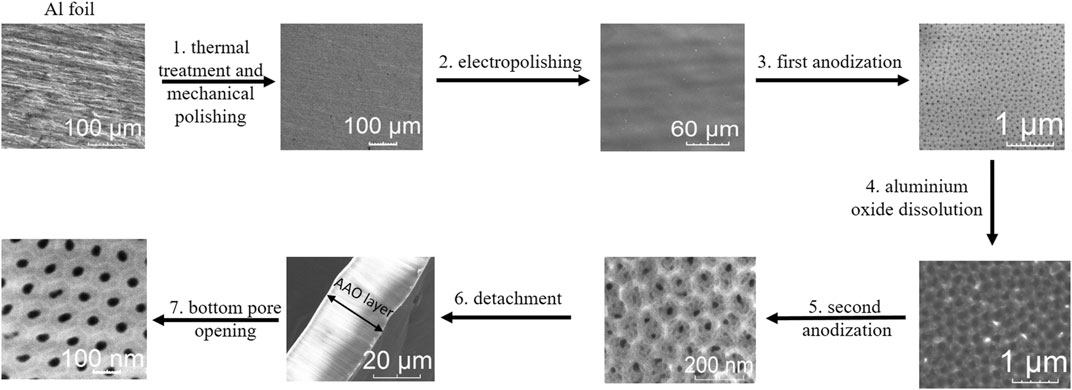
FIGURE 6. Anodization and detachment process scheme showing the fabrication steps from the original Al foil to anodic aluminium oxide (AAO) template.
Several parameters of the process have been optimized to obtain arrays of vertically aligned porous alumina. To establish the composition of the electrolyte solution, phosphoric acid was first used in the anodization process which resulted in not well-defined pore walls, while changing to the oxalic acid solution resulted in pores with straight walls. The anodization voltage allowed tuning the pores diameter, increasing the voltage resulting in an increase in their diameter. By increasing the anodization temperature, the chemical dissolution of oxide in the inner layer and the electrochemical formation of the anodic oxide layer are enhanced [39], resulting in a poor symmetry of the AAO template [40]. Also, a low temperature results in a slower growth rate of the AAO, thus fewer mechanical stresses [41], allowing the detachment of a defect-free, high-quality alumina free-standing layer; hence, 15°C was chosen as the optimum temperature. Moreover, the detachment method was adapted, by adjusting the time for each stair-like reverse bias and the electrolyte temperature, to suit the desired pores diameter and the thickness of the AAO template. A good reproducibility of the processes was observed, the samples showing good stability after long periods of time of storage at room temperature, in antistatic boxes.
The detached AAO is about 40 mm in length and 20 mm in width, with a thickness that can be varied between 5 and 100 μm. The AAO template density is around 2.7 g/cm3 and the porosity, defined as the ratio of the surface occupied by the pores to the whole surface area, is approximately 30%, for 40 nm pore diameter and 45 nm interpore distance. A focal spot of 5 μm focused on an AAO template characterized by these parameters would contain an average number of 3,000 pores. Using this technique, structures with pore sizes ranging from 10s to several hundreds of nm and aspect ratio up to 104 can be created, with a porosity up to 70% and a corresponding porous template density of around 1 g/cm3.
The SEM and AFM images of the detached AAO template are shown in Figure 7. A homogeneous pore distribution was obtained, with the diameter of the distributed cylindrical pores ranging from 30 to 60 nm, as illustrated in Figure 7A. The thickness of the rear side barrier layer is about 50 nm, as shown in the SEM cross-section image from Figure 7B, with a honeycomb arrangement (Figure 7C); an AFM 3D view of the barrier curvature being shown in Figure 7D. In Figure 7E, schematic 3D images of the AAO templates with open and closed bottom pores is presented.
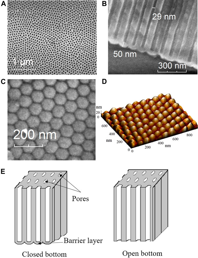
FIGURE 7. SEM images of anodic aluminium oxide: (A) front view, (B) cross-sectional view, and (C) rear view. (D) AFM 3D-image of rear side of alumina and (E) schematic representation of the AAO template (left, with barrier layer; right, without barrier layer).
For laser-driven experiments, the AAO template is cut into strips about 1 cm long and 1–2 mm wide, with a thickness ranging from 5 to 20 μm. Then, they are attached on a custom-made C-shape frame mounted on a stalk a few centimetres long (Figure 8A), and eventually assembled on a 16 positions target wheel which is used in the experimental setup. The final free-standing AAO targets can be delivered either with closed or opened bottom pores (i.e., both sides with pores exposed). During the experiment, before each shot, the target is precisely aligned in the required position with the help of an imaging system (Figure 8B). A laser probe beam, derived from the main beam, is used to probe the expanding plasma in the forward and backward directions by shadowgraphy and interferometry. Setting the proper delay between the probe beam and the main beam allows us to take snapshots of the plasma evolution during the interaction. Figure 8C shows a typical shadowgraph image of a 20 μm-thick free-standing AAO taken before shooting.
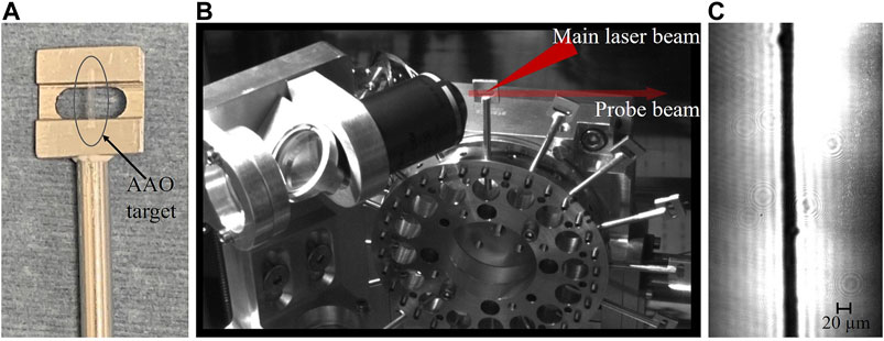
FIGURE 8. (A) Front side of the free-standing AAO mounted on a C-shaped Al-frame, prepared for assembly on the experimental setup. (B) Experimental setup showing the targets mounted on a rotating target wheel and the online imaging system used for laser focal spot optimization and target alignment. (C) Shadowgraph image of a 20 µm-thick free-standing AAO target aligned in shooting position.
Triangle-Like Metallic Patterns
Self-assembly of polystyrene (PE) microspheres into a structured monolayer has proved to be a low-cost time-efficient process, compared to standard electron beam lithography and photolithography techniques. This technique allows subsequent monolayer coating with one or multi-layered materials which, followed by chemical dissolution of PE beads, leads to customized ordered size-controlled arrays, of triangle-like shape or hemispherical cup-shaped microparticles. Used as such, PE microspheres proved to be effective on large surfaces as structured targets for laser-accelerated particles despite the highly diffractive nature of these structures [42]. In this matter, foils can be nanostructured by using an inexpensive, but versatile technique, of commercial polystyrene microspheres-assisted lithography [43]. Taking advantage of this technique, in this article, a solution containing 10 ± 0.5% polystyrene microspheres, with an average diameter of 3 µm (0.12 µm standard deviation), was deposited on 10 µm thick Au foils (placed on a Si substrate, as support) using drop-casting or dip-coating methods. The microspheres solution (Magsphere Inc.), containing an anionic surfactant, had 1.05 g/ml of polymer density.
The drop-casting method resulted in a monolayer of self-assembled polystyrene microspheres; in the second method, dip-coating, as described by J. Limpouch et al. [5], a rearrangement of the microspheres takes place on the surface of the water solution, followed by the recovery of the floating microsphere monolayer onto the metallic foil. The monolayer is then dried in air for solvent evaporation, resulting in the microspheres patterned foils, as shown in Figure 9A. Triangle-shaped metallic patterns can be obtained by depositing a gold layer via DC sputtering and then by mechanical or chemical removal of the beads. This final step exposes the remaining metallic microstructures formed between the microspheres, which served as a mask. The diameter of the microspheres is then the sole parameter in controlling both the spacing and the lateral dimensions of the micro/nanostructures. A 3D optical profilometry image, acquired in white-light interferometry mode, is presented in Figure 9B for the resulting Au microstructures arranged in an ordered hexagonally shaped array. Additional ongoing tests are currently being undertaken for improving the process for increased reproducibility for large area coverage, along with the implementation of the fabrication process on thinner Au and Cu foils. The aim is to obtain a better-controlled process for yielding increased reproducibility over a large area of high-quality ordered metallic microstructures on free-standing metallic foils. Moreover, for controlled low-field absorption tests, an updated scheme of the envisaged Au micro/nanoparticles structures including a dielectric layer is shown in Figure 9C. The metal–insulator–metal (MIM) multilayer leads to a significantly improved absorption (>98%) if specific dimensions/critical coupling conditions are fulfilled [44], the nanostructure acting as a Fabry–Pérot resonator cavity leading to a nearly perfect absorption. In addition, a variant of this technique can be employed to create hemispherical void structures (Figure 9D) that can be transferred on the front and/or backside of the free-standing foils [21, 45].
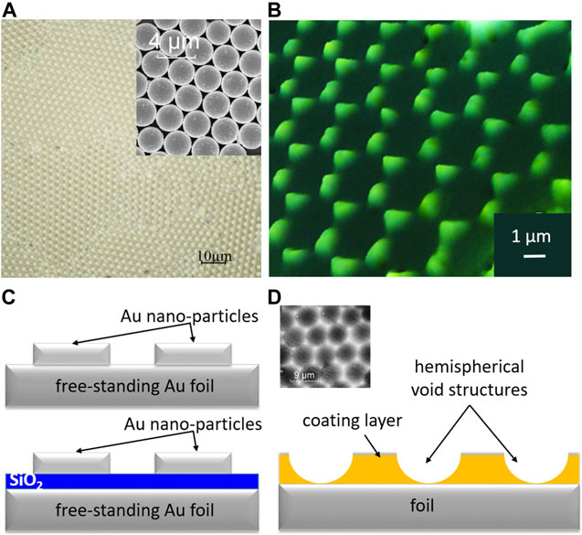
FIGURE 9. (A) Optical image of a monolayer of polystyrene microparticles deposited on metallic foil, (B) optical profilometry 3D image of Au microstructures created by microsphere assisted lithography, and (C) scheme of structures based on Au nanoparticles and Au MIM patterns. (D) Scheme of the hemispherical void structures that can be used on both target sides; (inset) the SEM image of 4.5 microns hemispherical voids.
Micro/Nanodots
Sub-wavelength structures (<800 nm) on the target surface can control laser reflection and improve energy absorption [46], but due to their reduced dimensions, they are more fragile to high laser pre-pulse; thus, additional consideration has to be provided to the laser parameters to protect these structures. In this regard, ordered metallic micro- and nanoscale dots (called micro/nanodots) have been obtained by a combination of EBL, metal deposition, and ion etching. Preliminary studies, described here, were performed on Si substrate for process optimization, with later on transfer of the process on thin free-standing metallic foils.
The manufacturing procedure is briefly described in Figure 10. Respectively, 150 nm-wide Au nanodots and 300 nm–1 µm-wide Cr dots have been obtained by exposing to the electron beam (25 kV voltage, 0.096 nA exposure current) the drawn pattern of the microdots in the positive PMMA resist, previously spin-coated onto a silicon wafer (1,000 rpm, ramp 20, 60 μL, 1 min, and ≈120 nm thickness). After the development of the exposed areas (MIBK:IPA solution 1:3), the surface was covered either by Au or Cr layer, deposited by e-beam evaporation (9 kV voltage, 2.5 × 10⁻⁷ mbar pressure; growth rates of 1.3 Å/s for Cr and 1.6 Å/s for Au, respectively), followed by lift-off procedure (in puddle acetone and ultrasound bath), resulting in a structured surface with metallic microdots. The thickness of the deposited metallic layer was chosen as one-third of the PMMA resist thickness to facilitate the lift-off process. For Au features, a 3 nm Ti layer was added as an adhesion promoter by e-beam deposition (0.8 Å/s growth rate, 60 mA current, and 9 kV voltage). Examples of the obtained metallic dots of different sizes are given in SEM images from Figure 11, for Au nanodots (Figure 11A,B) and Cr microdots (Figure 11C,D).
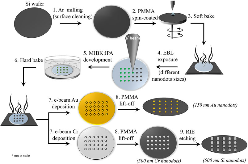
FIGURE 10. Patterning procedure scheme showing the fabrication steps of Au and Si nanodots, using Cr nanodots as a mask (representation not to scale).
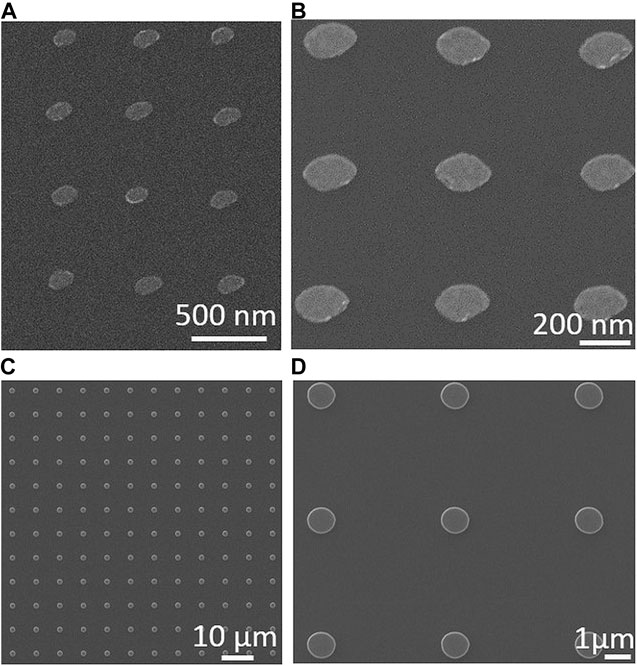
FIGURE 11. SEM images of (A,B) 150 nm-wide Au nanodots and (C,D) 1 µm-wide Cr microdots.
After the metallic micro/nanodots manufacturing process, using the obtained features as a mask in a supplemental etching step employing reactive ion etching (RIE), micron-sized elongated patterns have been successfully obtained (Figure 12). Specifically, arrays of 500 nm- or 300 nm-wide silicon microdots have been fabricated using different-sized Cr microdots as a mask. Experimental tests for the optimization parameters of the RIE process have revealed an optimum composition of 90:10 CHF3:O2, at 20°C, RF power 120 W, and a pressure of 0.1 mbar, leading to an etching rate of Si of 0.6 nm/s. In Figure 12, a selection of the SEM micrographs of the obtained Si microdots of 500 nm wide and 110 nm height is presented (Figures 12A,B), and 300 nm wide and 200 nm height (Figures 12C,D), respectively.
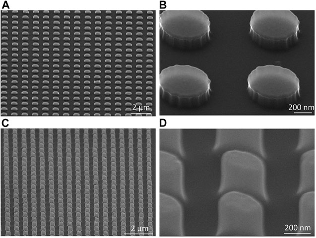
FIGURE 12. SEM micrographs of (A,B) 500 nm-wide and (C,D) 300 nm-wide Si microdots fabricated using Cr dots as a mask.
These nanostructures benefit from the highest possible geometrical control, allowed by e-beam or ion lithography, on relatively large surfaces [47]. This reflects into a high quality and reproducible type of structures. Once the process parameters have been optimized, to obtain the best quality of the structures (shape, sharp edges, precise spacing and dimensions, and homogeneous (regular) arrangement of the micro/nanodots), the reproducibility of these structures is ensured for a large number of samples. We can accurately control the diffraction channel of the structure through separation distance control, with nm precision. The interaction between such structures and the laser pulse, in particular the prepulse, can be tuned by changing the wavelength of their localized resonance via dimensions and material choice [48, 49].
As for the stability of these structured targets, Si and Au micro/nanodots are well known to be stable over long periods, while Cr microdots targets are recommended to be stored in controlled temperature and humidity conditions, as surface oxidation may occur.
Conclusion
We presented here research directions within ELI-NP for producing structured targets that can be used for more efficient coupling between high-intensity laser pulses and solid targets, and to improve the acceleration and the characteristics of the ion beams. As laser-plasma interaction at the target’s surface is sensitive to surface modulations, we developed several technologies for producing complex targets with structured surfaces. Micrometre- and nanometre-scale structures, such as periodic grating, metallic micro/nanodots, were fabricated on free-standing Cu and Au foils or on Si substrates by conventional techniques, such as electron-beam lithography and dry etching, or by microsphere assisted lithography. For surface ion acceleration, porous materials (alumina) were developed, using electrochemical methods. Ongoing research is directed towards optimizing the target’s design to allow their use in the foreseen high-power laser experiments.
Data Availability Statement
The original contributions presented in the study are included in the article; further inquiries can be directed to the corresponding author.
Author Contributions
CG: conceptualization, performed experimental work, formal analysis, writing the manuscript–original draft preparation, review, and editing; SI: performed the experimental work and editing the manuscript part on alumina; PG: conceptualization, review, and editing the manuscript; MC: review and editing the manuscript, performed experimental work; DD: conceptualization, review and editing the manuscript; DP: performed experimental work of mounting, assembly and frames and holders fabrication; VL: conceptualization, performed experimental work, formal analysis, review, and editing the manuscript.
Funding
The authors thank the support of the ELI-NP Phase II, a project co-financed by the Romanian Government and the European Union through the European Regional Development Fund - the Competitiveness Operational Program (1/July 07, 2016, COP, ID 1334). This work was also funded by the European Union Framework Programme for Research and Innovation Horizon 2020 under grant agreement No 871161; by the Romanian Government, under the National Program Installations and Strategic Objectives of National Interest and under the Nucleu project, grant no. PN19060105.
Conflict of Interest
The authors declare that the research was conducted in the absence of any commercial or financial relationships that could be construed as a potential conflict of interest.
Publisher’s Note
All claims expressed in this article are solely those of the authors and do not necessarily represent those of their affiliated organizations, or those of the publisher, the editors, and the reviewers. Any product that may be evaluated in this article, or claim that may be made by its manufacturer, is not guaranteed or endorsed by the publisher.
Acknowledgments
The authors would like to acknowledge Dr. Mirela Cerchez for fruitful discussions and suggestions and Dr. Mihai Cuciuc for the kind help with the electrochemical set-up.
References
1. Doria D, Cernaianu MO, Ghenuche P, Stutman D, Tanaka KA, Ticos C, et al. Overview of ELI-NP Status and Laser Commissioning Experiments with 1 PW and 10 PW Class-Lasers. J Inst (2020) 15:C09053. doi:10.1088/1748-0221/15/09/c09053
2. Bobeica M, Aogaki S, Asavei T, Cernaianu MO, Ghenuche P, Stutman D. Dose Calculations in a Cell Monolayer for High-Throughput Irradiation with Proton Beams Generated by PW Lasers for Space Applications. Life Sci Space Res (2018) 19:68–75. doi:10.1016/j.lssr.2018.10.003
3. Asavei T, Tomut M, Bobeica M, Aogaki S, Cernaianu M, Ganciu M, et al. Materials in Extreme Environments for Energy, Accelerators and Space Applications at ELI-NP. Rom Rep Phys (2016) 68:S275–S347.
4. Margarone D, Klimo O, Kim IJ, Prokůpek J, Limpouch J, Jeong TM, et al. Laser-Driven Proton Acceleration Enhancement by Nanostructured Foils. Phys Rev Lett (2012) 109:234801. doi:10.1103/PhysRevLett.109.234801
5. Limpouch J, Klimo O, Psikal J, Proska J, Novotný F, Margarone D, et al. Efficient Ion Beam Generation in Laser Interactions with Micro-structured Targets. EPJ Web of Conferences (2013) 59:17011. doi:10.1051/epjconf/20135917011
6. Dalui M, Wang W-M, Trivikram TM, Sarkar S, Tata S, Jha J, et al. Preferential Enhancement of Laser-Driven Carbon Ion Acceleration from Optimized Nanostructured Surfaces. Sci Rep (2015) 5:11930. doi:10.1038/srep11930
7. Ceccotti T, Floquet V, Sgattoni A, Bigongiari A, Klimo O, Raynaud M, et al. Evidence of Resonant Surface-Wave Excitation in the Relativistic Regime through Measurements of Proton Acceleration from Grating Targets. Phys Rev Lett (2013) 111:185001. doi:10.1103/PhysRevLett.111.185001
8. Nagai K, Musgrave CSA, Nazarov W. A Review of Low Density Porous Materials Used in Laser Plasma Experiments. Phys Plasmas (2018) 25:030501. doi:10.1063/1.5009689
9. Kar S, Markey K, Borghesi M, Carroll DC, McKenna P, Neely D, et al. Ballistic Focusing of Polyenergetic Protons Driven by Petawatt Laser Pulses. Phys Rev Lett (2011) 106:225003. doi:10.1103/PhysRevLett.106.225003
10. Kaymak V, Aktan E, Cerchez M, Elkin B, Papenheim M, Prasad R, et al. Boosted Acceleration of Protons by Tailored Ultra-thin Foil Targets. Sci Rep (2019) 9:18672. doi:10.1038/s41598-019-55011-2
11. Schwoerer H, Pfotenhauer S, Jäckel O, Amthor K-U, Liesfeld B, Ziegler W, et al. Laser-plasma Acceleration of Quasi-Monoenergetic Protons from Microstructured Targets. Nature (2006) 439:445–8. doi:10.1038/nature04492
12. Negoita F, Roth M, Thirolf P, Tudisco S, Hannachi F, Moustaizis SD, et al. Laser Driven Nuclear Physics at ELI-NP. Rom Rep Phys (2016) 68:S37.
13. Lureau F, Matras G, Chalus O, Derycke C, Morbieu T, Radier C, et al. High-energy Hybrid Femtosecond Laser System Demonstrating 2 × 10 PW Capability. High Pow Laser Sci Eng (2020) 8:e43. doi:10.1017/hpl.2020.41
14. Gales S, Tanaka KA, Balabanski DL, Negoita F, Stutman D, Tesileanu O, et al. The Extreme Light Infrastructure-Nuclear Physics (ELI-NP) Facility: New Horizons in Physics with 10 PW Ultra-intense Lasers and 20 MeV Brilliant Gamma Beams. Rep Prog Phys (2018) 81:094301. doi:10.1088/1361-6633/aacfe8
15. Tanaka KA, Spohr KM, Balabanski DL, Balascuta S, Capponi L, Cernaianu MO, et al. Current Status and Highlights of the ELI-NP Research Program. Matter Radiat Extremes (2020) 5:024402. doi:10.1063/1.5093535
16. Purvis MA, Shlyaptsev VN, Hollinger R, Bargsten C, Pukhov A, Prieto A, et al. Relativistic Plasma Nanophotonics for Ultrahigh Energy Density Physics. Nat Photon (2013) 7:796–800. doi:10.1038/nphoton.2013.217
17. Picciotto A, Margarone D, Crivellari M, Bellutti P, Colpo S, Torrisi L, et al. Microfabrication of Silicon Hydrogenated Thin Targets for Multi-MeV Laser-Driven Proton Acceleration. Appl Phys Express (2011) 4:126401. doi:10.1143/apex.4.126401
18. Spindloe C, Arthur G, Hall F, Tomlinson S, Potter R, Kar S, et al. High Volume Fabrication of Laser Targets Using MEMS Techniques. J Phys Conf Ser (2016) 713:012002. doi:10.1088/1742-6596/713/1/012002
19. Prencipe I, Fuchs J, Pascarelli S, Schumacher DW, Stephens RB, Alexander NB, et al. Targets for High Repetition Rate Laser Facilities: Needs, Challenges and Perspectives. High Pow Laser Sci Eng (2017) 5:e17. doi:10.1017/hpl.2017.18
20. Giuffrida L, Svensson K, Psikal J, Dalui M, Ekerfelt H, Gallardo Gonzalez I, et al. Manipulation of Laser-Accelerated Proton Beam Profiles by Nanostructured and Microstructured Targets. Phys Rev Accel Beams (2017) 20:81301. doi:10.1103/PhysRevAccelBeams.20.081301
21. Habara H, Lad AD, Nagami R, Singh PK, Chatterjee G, Adak A, et al. Micro-optics for Ultra-intense Lasers. AIP Adv (2021) 11:035214. doi:10.1063/5.0038023
22. Klimo O, Psikal J, Limpouch J, Proska J, Novotny F, Ceccotti T, et al. Short Pulse Laser Interaction with Micro-structured Targets: Simulations of Laser Absorption and Ion Acceleration. New J Phys (2011) 13:053028. doi:10.1088/1367-2630/13/5/053028
23. Gheorghiu CC, Leca V, Popa D, Cernaianu MO, Stutman D. Overview on the Target Fabrication Facilities at ELI-NP and Ongoing Strategies. J Inst (2016) 11:C10011. doi:10.1088/1748-0221/11/10/c10011
24. Macchi A, Cantono G, Fedeli L, Pisani F, Ceccotti T. Extreme High Field Plasmonics: Electron Acceleration and XUV Harmonic Generation from Ultrashort Surface Plasmons. Phys Plasmas (2019) 26:042114. doi:10.1063/1.5086537
25. Fedeli L, Sgattoni A, Cantono G, Garzella D, Réau F, Prencipe I, et al. Electron Acceleration by Relativistic Surface Plasmons in Laser-Grating Interaction. Phys Rev Lett (2016) 116:15001. doi:10.1103/PhysRevLett.116.015001
26. Cerchez M, Prasad R, Aurand B, Giesecke AL, Spickermann S, Brauckmann S, et al. ARCTURUS Laser: a Versatile High-Contrast, High-Power Multi-Beam Laser System. High Pow Laser Sci Eng (2019) 7:e37. doi:10.1017/hpl.2019.21
27. Gheorghiu CC, Cerchez M, Aktan E, Prasad R, Yilmaz F, Yilmaz N, et al. 2021 Fabrication of Micron-Size Periodic Gratings in Free-Standing Metallic Foils for Enhanced Laser Energy Absorption. submitted to High Power Laser Science and Engineering
28. Jiang S, Krygier AG, Schumacher DW, Akli KU, Freeman RR. Enhancing Bremsstrahlung Production from Ultraintense Laser-Solid Interactions with Front Surface Structures. Eur Phys J D (2014) 68:283. doi:10.1140/epjd/e2014-50339-4
29. Jiang S, Krygier AG, Schumacher DW, Akli KU, Freeman RR. Effects of Front-Surface Target Structures on Properties of Relativistic Laser-Plasma Electrons. Phys Rev E (2014) 89:13106. doi:10.1103/PhysRevE.89.013106
30. Jiang S, Ji LL, Audesirk H, George KM, Snyder J, Krygier A, et al. Microengineering Laser Plasma Interactions at Relativistic Intensities. Phys Rev Lett (2016) 116:85002. doi:10.1103/PhysRevLett.116.085002
31. Vallières S, Salvadori M, Permogorov A, Cantono G, Svendsen K, Chen Z, et al. Enhanced Laser-Driven Proton Acceleration Using Nanowire Targets. Sci Rep (2021) 11:2226. doi:10.1038/s41598-020-80392-0
32. Samsonova Z, Höfer S, Kaymak V, Ališauskas S, Shumakova V, Pugžlys A, et al. Relativistic Interaction of Long-Wavelength Ultrashort Laser Pulses with Nanowires. Phys Rev X (2019) 9:21029. doi:10.1103/PhysRevX.9.021029
33. Dozières M, Petrov GM, Forestier-Colleoni P, Campbell P, Krushelnick K, Maksimchuk A, et al. Optimization of Laser-Nanowire Target Interaction to Increase the Proton Acceleration Efficiency. Plasma Phys Control Fusion (2019) 61:065016. doi:10.1088/1361-6587/ab157c
34. Jessensky O, Müller F, Gösele U. Self-organized Formation of Hexagonal Pore Arrays in Anodic Alumina. Appl Phys Lett (1998) 72:1173–5. doi:10.1063/1.121004
35. Roslyakov IV, Gordeeva EO, Napolskii KS. Role of Electrode Reaction Kinetics in Self-Ordering of Porous Anodic Alumina. Elsevier (2017). doi:10.1016/j.electacta.2017.04.140
36. Gâlcă AC, Kooij ES, Wormeester H, Salm C, Leca V, Rector JH, et al. Structural and Optical Characterization of Porous Anodic Aluminum Oxide. J Appl Phys (2003) 94:4296–305. doi:10.1063/1.1604951
37. Ahmad N, khan S, Arman liaqat M, Awais M, Shah SA, Ahmed I, et al. Influence of Voltage Variation on Structure and Magnetic Properties of Co1−x Sn X (X = 0.3-0.7) Nanowire Alloys in Alumina by Electrochemical Deposition. Appl Phys A (2017) 123:1–7. doi:10.1007/s00339-016-0682-7
38. Hong YK, Kim BH, Kim DI, Park DH, Joo J. High-yield and Environment-Minded Fabrication of Nanoporous Anodic Aluminum Oxide Templates. RSC Adv (2015) 5:26872–7. doi:10.1039/c5ra00198f
39. Sulka GD. Highly Ordered Anodic Porous Alumina Formation by Self-Organized Anodizing (2008). p. 1–116. doi:10.1002/9783527621507.ch1
40. Ba L, Li WS. Influence of Anodizing Conditions on the Ordered Pore Formation in Anodic Alumina. J Phys D: Appl Phys (2000) 33:2527–31. doi:10.1088/0022-3727/33/20/302
41. Jeong SH, Im HL, Hong S, Park H, Baek J, Park DH, et al. Massive, Eco-Friendly, and Facile Fabrication of Multi-Functional Anodic Aluminum Oxides: Application to Nanoporous Templates and Sensing Platforms. RSC Adv (2017) 7:4518–30. doi:10.1039/C6RA25201J
42. Margarone D, Kim IJ, Psikal J, Kaufman J, Mocek T, Choi IW, et al. Laser-driven High-Energy Proton Beam with Homogeneous Spatial Profile from a Nanosphere Target. Phys Rev ST Accel Beams (2015) 18:71304. doi:10.1103/PhysRevSTAB.18.071304
43. Kasim J, Ting Y, Meng YY, Ping LJ, See A, Jong LL, et al. Near-field Raman Imaging Using Optically Trapped Dielectric Microsphere. Opt Express (2008) 16:7976–84. doi:10.1364/OE.16.007976
44. Cattoni A, Ghenuche P, Haghiri-Gosnet A-M, Decanini D, Chen J, Pelouard J-L, et al. λ3/1000 Plasmonic Nanocavities for Biosensing Fabricated by Soft UV Nanoimprint Lithography. Nano Lett (2011) 11:3557–63. doi:10.1021/nl201004c
45. Chen T, Chang DP, Jordan R, Zauscher S. Colloidal Lithography for Fabricating Patterned Polymer-brush Microstructures. Beilstein J Nanotechnol (2012) 3:397–403. doi:10.3762/bjnano.3.46
46. Barberio M, Scisciò M, Veltri S, Antici P. Fabrication of Nanostructured Targets for Improved Laser-Driven Proton Acceleration. Superlattices and Microstructures (2016) 95:159–63. doi:10.1016/j.spmi.2016.04.023
47. Chen Y. Nanofabrication by Electron Beam Lithography and its Applications: A Review. Microelectronic Eng (2015) 135:57–72. doi:10.1016/j.mee.2015.02.042
48. Fernández-Domínguez AI, García-Vidal FJ, Martín-Moreno L. Unrelenting Plasmons. Nat Photon (2017) 11:8–10. doi:10.1038/nphoton.2016.258
Keywords: structured targets, fabrication, optimization, free-standing, enhanced acceleration mechanism
Citation: Gheorghiu CC, Ionescu SC, Ghenuche P, Cernaianu MO, Doria D, Popa D and Leca V (2021) Structuring Free-Standing Foils for Laser-Driven Particle Acceleration Experiments. Front. Phys. 9:727498. doi: 10.3389/fphy.2021.727498
Received: 18 June 2021; Accepted: 24 August 2021;
Published: 29 September 2021.
Edited by:
Daniele Margarone, Queen’s University Belfast, United KingdomReviewed by:
Giada Cantono, Lund University, SwedenAntonino Picciotto, Bruno Kessler Foundation, Italy
Copyright © 2021 Gheorghiu, Ionescu, Ghenuche, Cernaianu, Doria, Popa and Leca. This is an open-access article distributed under the terms of the Creative Commons Attribution License (CC BY). The use, distribution or reproduction in other forums is permitted, provided the original author(s) and the copyright owner(s) are credited and that the original publication in this journal is cited, in accordance with accepted academic practice. No use, distribution or reproduction is permitted which does not comply with these terms.
*Correspondence: Victor Leca, dmljdG9yLmxlY2FAZWxpLW5wLnJv