 Francesco Gramuglia1†*
 Emanuele Ripiccini1†
 Carlo Alberto Fenoglio1Ming-Lo Wu1Lorenzo Paolozzi2,3Claudio Bruschini1‡
 Edoardo Charbon1‡
- 1Advanced Quantum Architecture Laboratory, Ecole Polytechnique Fédérale de Lausanne (EPFL), Neuchatel, Switzerland
- 2Departement de Physique Nucléaire et Corpusculaire, Université de Genève, Geneva, Switzerland
- 3European Organization for Nuclear Research, CERN, Meyrin, Switzerland
Major advances in silicon pixel detectors, with outstanding timing performance, have recently attracted significant attention in the community. In this work we present and discuss the use of state-of-the-art Geiger-mode APDs, also known as single-photon avalanche diodes (SPADs), for the detection of minimum ionizing particles (MIPs) with best-in-class timing resolution. The SPADs were implemented in standard CMOS technology and integrated with on-chip quenching and recharge circuitry. Two devices in coincidence allowed to measure the time-of-flight of 180 GeV/c momentum pions with a coincidence time resolution of 22 ps FWHM (9.4 ps Gaussian sigma). Radiation hardness measurements, also presented here, highlight the suitability of this family of devices for a wide range of high energy physics (HEP) applications.
1 Introduction
1.1 High Timing Resolution With Silicon Pixel Detectors
Silicon pixel detectors have been developed in high-energy physics applications to provide precise position measurements thanks to their compactness and high spatial granularity. Recent developments have been focused on sub-100 ps timing measurements of optical photons and direct detection of charged particles.
When a particle passes through the detector, electron-hole pairs are generated. When these charges move in the depletion region, an induced current pulse is registered on one electrode. According to the Schockley-Ramo theorem [1, 2], this current is proportional to the free charge Q, to the speed of the charge carriers v, and to the weighting field, which can be expressed, to a first approximation, as
where k is a proportionality factor. The signal ends when all charges have been collected. Moreover, in case of a minimum ionizing particle (MIP) crossing a thin device, the charge Q is proportional to d. We thus have:
where N is the number of electron-hole pairs generated per unit length. This result shows that the initial value of the induced current is constant and does not depend on the thickness of the depletion region. When reading out this current signal on a load, behaving like an ideal transimpedance amplifier, we observe a sharp voltage pulse. The time-of-arrival of the charge is usually determined by comparing the voltage pulse with a threshold. The uncertainty of the voltage pulse σV is expressed as:
where σt is the timing jitter of the voltage pulse. By inverting Eq. 3, we find that:
Equation 4 shows that the signal fluctuation (σV) should be reduced to achieve a better timing jitter σt and the slew rate
All the effects mentioned above call for extremely high intrinsic gain and slew rate together with thin structures. Thus, Geiger-mode silicon APDs (i.e., devices biased above breakdown), also known as single-photon avalanche diodes (SPADs), could represent promising candidates for substantial timing jitter reduction [11]. In SPADs, unlike APDs, the avalanche is a self-sustaining process, and the timing jitter contributions are more related to the avalanche growth dynamics. In particular, the timing jitter improves, decreasing the avalanche current value needed by the frontend electronics to detect a pulse [12]. A comprehensive theoretical study of timing performance in SPADs when used in MIP detection is presented in [13]. First examples of such systems, detailed in [14–16], were following the concept proposed by [17].
Although these potential advantages are promising, some problems usually affect Geiger-mode devices in the framework of MIP detection. Indeed, typical SPADs have a long dead time if no properly designed active quenching and recharge techniques are used [18]. Another issue is the presence of noise in the form of spurious pulses even in the dark. This noise, known as dark count rate (DCR), could limit the suitability of SPADs for the target application because of significant degradation of the measurement signal-to-noise ratio (SNR). However, as shown by [19, 20], DCR can be drastically reduced by detecting MIPs with two SPADs operated in coincidence. Building on these elements, we present MIP time-of-flight (ToF) measurements resulting in unprecedented timing precision.
1.2 Single-Photon Avalanche Diodes Detector and System-On-Board
The detector system used in this work relies on the SPAD-based sensor presented in [21]. This device’s cross-section is based on a substrate-isolated type, where a p-well (PW) layer forms the anode of the SPAD and a buried n-well (BNW) layer creates the cathode contact. The latter is connected to the high voltage through a deep-n-well (DNW). The SPAD presents a p-i-n structure [21]. Figure 1A shows the cross-section of the SPAD, while Figure 1B shows a micrograph of the sensor used in this study. The guard ring has a virtual design and employs a low doping p-Epi region located between the PW and the DNW contact to smooth the doping transition and lower the electric field. Thus, a p-Epi layer between anode and cathode allows a relatively extended and uniform high-field region (Figure 2A).
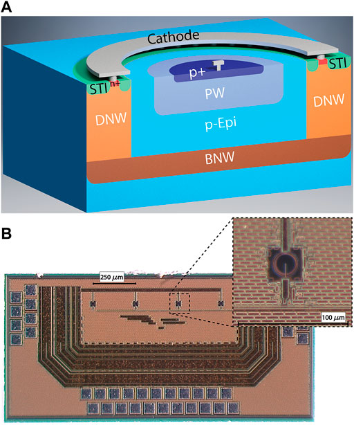
FIGURE 1. (A): SPAD cross section. (B): Micrograph of the implemented chip embedding 25 μm diameter SPADs with integrated pixel circuit [21].
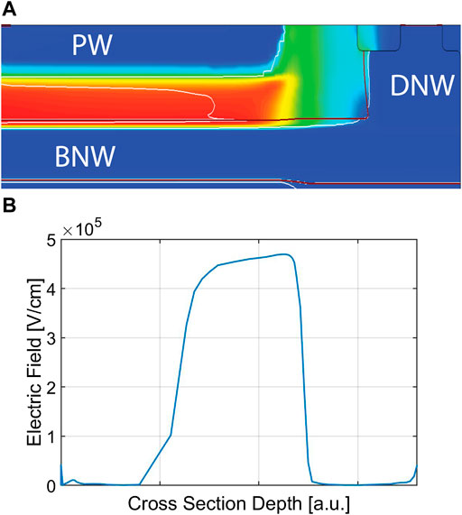
FIGURE 2. TCAD simulation of the 2D electric field distribution in the cross section (A). A quantification of the electric field along the vertical axis is also shown (B) [21].
The sensor integrates four independent SPAD pixels with a diameter of 25 μm. A dedicated on-chip front-end circuitry, shown in Figure 3, is implemented in close proximity to each SPAD. In the SPAD front-end circuit (see Figure 3) the cascode transistor M1 is used as a resistive divider and voltage clamp, along with M2 to enable high excess bias. This comes in combination with thin-oxide MOS transistors in the remainder of the front-end to improve the timing performance. M2 and M3 form the active recharge branch, turned on by the feedback loop composed by the NOR gate, Schmitt trigger, and tunable delay element (see Figure 3 right). The circuit is designed to enable a tunable dead time, as short as 3 ns, supporting very high count rates while still maintaining very low afterpulsing [21]. Concerning the leakage current for this detector, as reported in [21], the measured value is on the order of 0.1–1 pA, which corresponds to a value of about 0.4-4 fA/μm2.
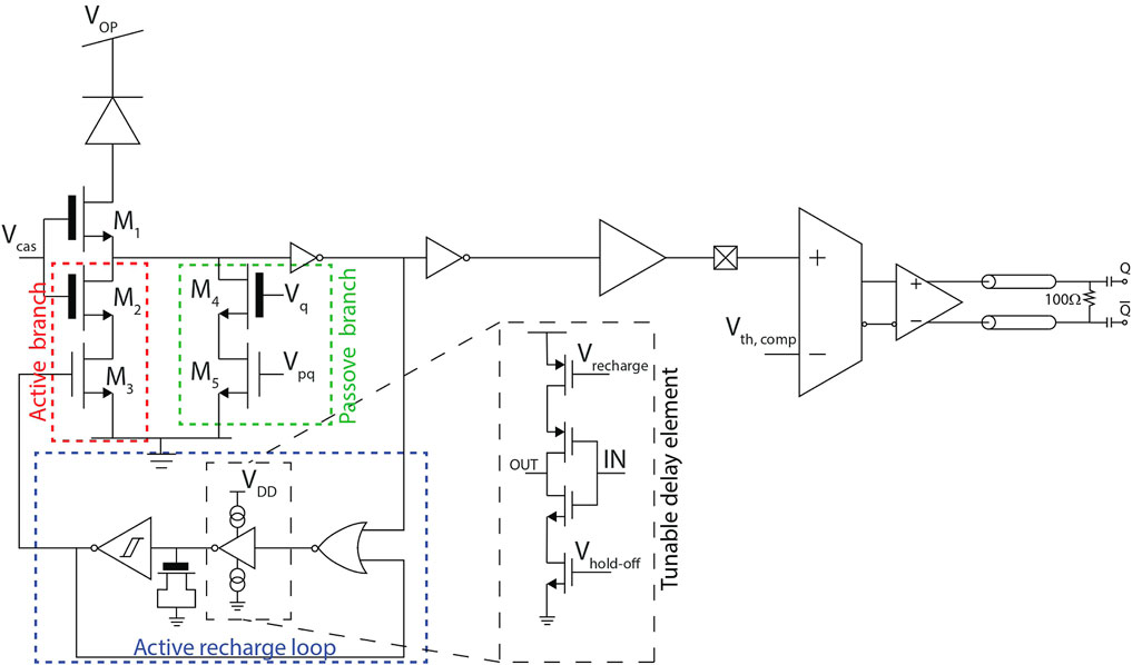
FIGURE 3. Device schematic. The chip output is connected to an external fast SiGe comparator to drive a 50 Ω differential output line.
In this work, we implemented a complete and optimized system-on-board to further improve performance. The resulting system comprises a motherboard, where all needed voltage levels are derived from a single 5 V power supply. A power management unit was designed to filter most of the electronic noise and to provide low-noise and stable voltage levels to the detector and its front-end circuits. Moreover, the full integration of a system-on-board reduces the noise picked up in cables and power cords that can act as antennas. Indeed, reducing the noise in the system is essential when the target timing precision approaches 10 ps [3]. A full system control is achieved with a serial bus interface that allows the tuning of the device operating point from an host computer.
The output of the chip is connected to fast SiGe comparators (Analog Device ADCMP572) that drive 50 Ω lines (Figure 3). This solution reduces the capacitive load at the chip’s output (high impedance node) and helps propagate the signal through a high-frequency cable to the timestamping electronics. In addition, the use of these comparators makes it possible to achieve high signal slew rate (≥1.6 V/ns).
2 Optical Device Characterization
In order to analyze the performance of our system, we started from an optical characterization using the setup in Figure 4 [21, 22]. The test bench is composed of a femtosecond pulsed laser used as the controlled light source, making the pulse length contribution to the measured timing jitter negligible. The laser beam is split into two branches. One branch is captured by a fast photodiode used as an optical, rather than electrical, reference to ensure that the dominant jitter is that of the device under test (DUT). The other branch passes through a second harmonic generation (SHG) stage to generate a light pulse in the visible range (i.e., within our device sensitivity spectrum). The latter is then attenuated, employing a neutral density filter (NDF) to reach a single-photon regime, and sent to the DUT. Finally, the output signals of the photodiode and the DUT are connected to an oscilloscope to build a time-difference histogram, representing the instrument response function (IRF). An asymmetric curve characterizes the typical SPAD IRF with the main peak, generally modeled with a Gaussian profile and an exponential tail [23–25].
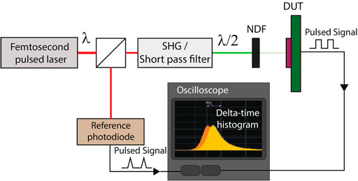
FIGURE 4. Experimental setup for device characterization using femtosecond pulsed lasers.
The experiment has been repeated for several excess bias voltages and two wavelengths, and the results are shown in Figure 5. The timing results are expressed as FWHM of the IRF. The timing precision shows a dependency on the bias point, and it improves when increasing the applied voltage, as expected. With this improved system, we reached a timing jitter of 7.5 ps at a reverse bias voltage of 28 V, corresponding to an excess bias (Vex) of about 6.5 V. Moreover, we report in Figure 5B the decay time constant of the exponential tail again as a function of reverse bias voltage. These results show an improvement of almost 40% with respect to what reported in [21], where the output was directly taken from the packaged die with high impedance 4 GHz active probes. This optical characterization provides us with an estimation of the system performance when detecting a MIP. Indeed, the mean free path of a MIP in silicon is on the order of hundreds of nanometers. Therefore, considering the thin structure of the proposed SPADs, we expect the generation of a small amount of primary charge inside the device sensitive volume. Moreover, Geiger-mode operation and a prompt avalanche detection ensure that the output signal is the same when detecting single photons or MIPs.
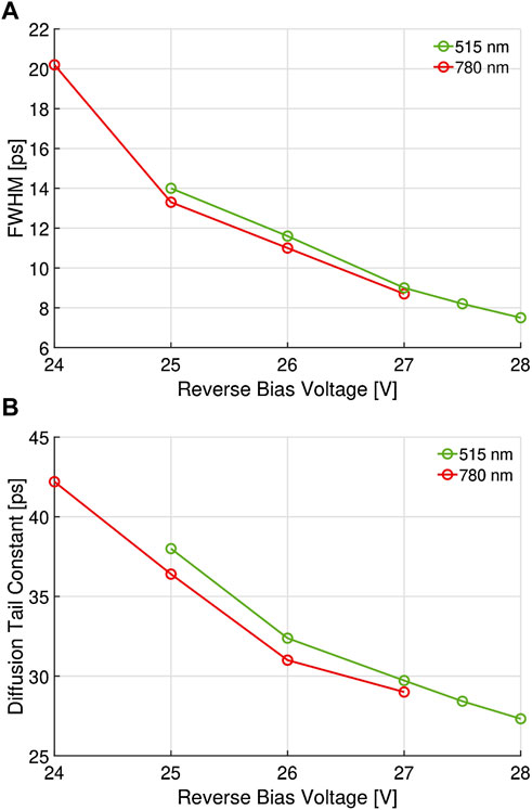
FIGURE 5. (A) FWHM single-photon timing resolution obtained with the designed system. (B) Exponential tail time constant measured at various excess bias voltages. For these experiments two wavelengths were used: 515 and 780 nm. The results show a timing jitter of ∼7.5 ps FWHM for green and ∼8.5 ps FWHM for red light at ∼6.5 V of excess bias voltage.
3 Time-Of-Flight Measurements for Minimum Ionizing Particles
The setup used for the ToF measurement of MIPs is shown in Figure 6. It consists of two systems-on-board (see Section 1.2), both mounted on motorized linear stages with sub-micrometer positioning resolution to allow a proper detector alignment and to guarantee the acquisition of coincidence measurements. We installed the setup on the H8 beamline in the CERN North Area. This beamline delivers 180 GeV/c momentum pions produced on a graphite target by the interaction of protons accelerated by the Super Proton Synchrotron (SPS).
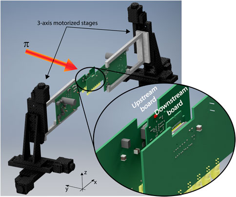
FIGURE 6. Experimental MIP coincidence measurement setup.
The beam profile measurement is reported in Figure 7. A good alignment between the two detectors has been achieved thanks to an HVCMOS telescope [26]. The two detectors were positioned at the center of the beam, where the intensity is the highest. Coincidence events were acquired for two bias voltages, 24 and 27 V, corresponding to approximately 2.5 and 5.5 V Vex, respectively. Figure 8 shows the ToF distributions for both Vex. The MIP measurement results are summarized in Table 1.
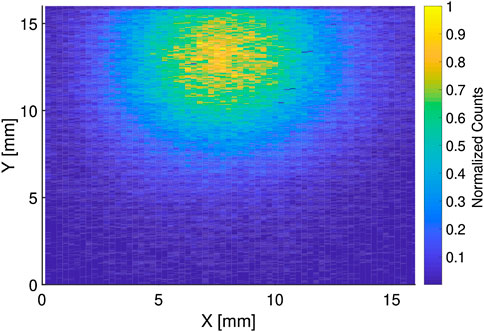
FIGURE 7. MIP beam profile acquired with the HVCMOS telescope described in [26].
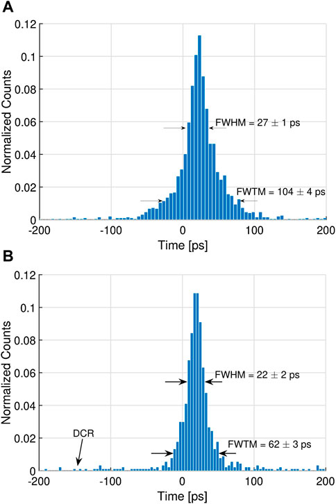
FIGURE 8. Normalized distribution of the MIP time-of-flight between two SPADs in coincidence. (A) at 24 V and (B) at 27 V bias voltage.
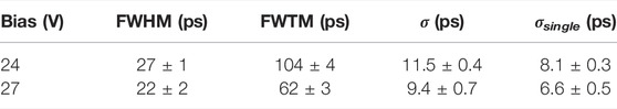
TABLE 1. Summary of the MIP detection measurement results. The Gaussian sigma has been obtained by dividing the FWHM by
4 Radiation Hardness
The radiation hardness of the SPAD detectors was characterized by using protons to induce ionizing damage and, more importantly, displacement damage, which causes structural permanent defects [27, 28]. The detectors were irradiated using the Proton Irradiation Facility (PIF) at the Paul Scherrer Institute (PSI, Villigen, Switzerland). We used a 100 MeV mono-energetic beam with a fluence of 1 × 10⁸ protons per second to reach a 300 TeV/g displacement damage dose (DDD) and 9.4 krad total ionizing dose (TID). The DCR difference was measured 2 weeks after the exposure with the aforementioned setup. The DCR comparison before and after the exposure is reported in Figure 9. The characterization of the radiation hardness shows that the SPAD detector can maintain its functionality under the given radiation dose. The SPADs are not saturated by the DCR induced by the radiation damage thanks to their short dead time and high count rate. Moreover, as the ToF measurement is based on coincidence, even detectors reaching a DCR value of 1 × 10⁵ counts per second will not affect their particle detection performance, as also shown in [19, 20]. No other degradation of the device performance was observed.
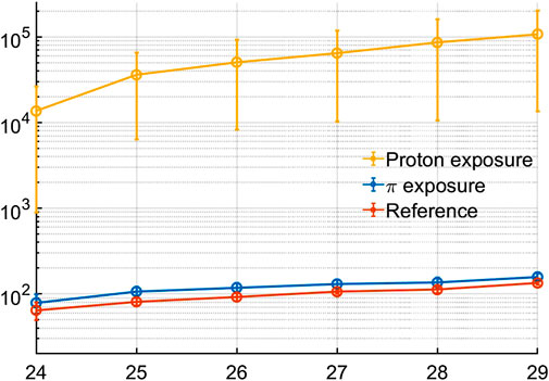
FIGURE 9. Radiation hardness experimental results (mean values on four devices). DCR trends over various excess bias voltages are reported. The reference with no irradiation (orange) is compared with the noise level after 100 MeV proton irradiation (yellow), and with the samples after 1 week of 180 GeV/c pions irradiation.
5 Discussion
In this work we showed how Geiger-mode devices (i.e., SPADs) can detect MIPs with a sub-10 ps timing precision. This result paves the way to the implementation of future high timing resolution particle trackers based on this kind of detector. Moreover, the radiation hardness of the device was explored up to a DDD of 300 TeV/g. After exposure, DCR increased by about three orders of magnitude, which is comparable with [29]. Nevertheless, this increment does not affect the timing performance of the device and does not cause the saturation of its output, thanks to the short dead time of 3 ns guaranteed by the integrated pixel circuit on-chip. In addition, while detecting charged particles on a beamline, the number of accidental coincidences due to DCR is strongly suppressed by the logic AND between the two SPADs used for the ToF measurement [19]. As shown in Section 1.2, in the proposed SPAD, the electric field is designed in order to have a uniform profile within the entire intrinsic layer, representing the multiplication region. Moreover, the small thickness of the charge collector region significantly reduces the charge collection noise. This two device features together with an improved front-end circuit and a maximization of the signal slew-rate are crucial when targeting sub-10 ps timing resolution.
When analyzing Figure 8 and the results in Table 1, we notice a dependency of the performance on the applied bias voltage. In particular, we can see a lower FWTM (full width at tenth maximum) and an improvement in the FWHM for the ToF distribution when increasing the bias point from 24 to 27 V. The higher field improves the avalanche buildup and lateral spread time dispersion [30–32]. Moreover, a higher bias voltage enlarges the drift region and increases the electric field inside it. This effect reduces the size of the neutral region and helps minimize the statistical spread of the diffusion and transit time needed by the primary charge carriers to reach the multiplication region [11].
Both distributions show a negligible flat background coming from random dark count coincidences. This is indicative of the efficacy of the noise filtering provided by measurements in coincidence.
Author Contributions
FG: Chip and board design, optical measurements, beam time measurements, data analysis, paper writing ER: ToF measurement with SPADs proposal, mechanical integration, data analysis, beam time measurements, paper writing CAF:Optical measurements, beam time measurements, data analysis, paper writing M-LW: radiation hardness measurements, data analysis, paper writing LP: Operation of the HV-CMOS telescope for SPADs alignment on beam, paper reviewing EC: Supervision, funding acquisition, paper reviewing CB: Supervision, funding acquisition, paper reviewing.
Funding
This research was supported, in part, by the Swiss National Science Foundation under grant 200021-169465 and Sinergia CRSII5-177165.
Conflict of Interest
The authors declare that the research was conducted in the absence of any commercial or financial relationships that could be construed as a potential conflict of interest.
Publisher’s Note
All claims expressed in this article are solely those of the authors and do not necessarily represent those of their affiliated organizations, or those of the publisher, the editors and the reviewers. Any product that may be evaluated in this article, or claim that may be made by its manufacturer, is not guaranteed or endorsed by the publisher.
Acknowledgments
We would like to thank the FASER group of the DPNC of the University of Geneva, led by Iacobucci, for the help and the support during the beamtime.
References
1. Shockley W. Currents to Conductors Induced by a Moving Point Charge. J Appl Phys (1938) 9:635–6. doi:10.1063/1.1710367
2. Ramo S. Currents Induced by Electron Motion. Proc IRE (1939) 27:584–5. doi:10.1109/jrproc.1939.228757
3. Cartiglia N, Baselga M, Dellacasa G, Ely S, Fadeyev V, Galloway Z, et al. Performance of Ultra-fast Silicon Detectors. J Inst (2014) 9:C02001. doi:10.1088/1748-0221/9/02/c02001
4. Cartiglia N, Arcidiacono R, Baselga M, Bellan R, Boscardin M, Cenna F, et al. Design Optimization of Ultra-fast Silicon Detectors. Nucl Instr Methods Phys Res Section A: Acc Spectrometers, Detectors Associated Equipment (2015) 796:141–8. doi:10.1016/j.nima.2015.04.025
5. Cartiglia N, Arcidiacono R, Ferrero M, Mandurrino M, Sadrozinski H-FW, Sola V, et al. Timing Layers, 4- and 5-dimension Tracking. Nucl Instr Methods Phys Res Section A: Acc Spectrometers, Detectors Associated Equipment (2019) 924:350–4. doi:10.1016/j.nima.2018.09.157
6. Cartiglia N, Staiano A, Sola V, Arcidiacono R, Cirio R, Cenna F, et al. Beam Test Results of a 16 Ps Timing System Based on Ultra-fast Silicon Detectors. Nucl Instr Methods Phys Res Section A: Acc Spectrometers, Detectors Associated Equipment (2017) 850:83–8. doi:10.1016/j.nima.2017.01.021
7. Paolozzi L. Development of Particle Detectors and Related Front End Electronics for Sub-nanosecond Time Measurement in High Radiation Environment. Ph.D. thesis. Rome, Italy: Roma Tor Vergata (2015).
8. Jadhav M, Armstrong W, Cloet I, Joosten S, Mazza SM, Metcalfe J, et al. Picosecond Timing Resolution Measurements of Low Gain Avalanche Detectors with a 120 GeV Proton Beam for the TOPSiDE Detector Concept. J Inst (2021) 16:P06008. doi:10.1088/1748-0221/16/06/p06008
9. Lai A, Anderlini L, Aresti M, Bizzeti A, Cardini A, Betta G-FD, et al. First Results of the TIMESPOT Project on Developments on Fast Sensors for Future Vertex Detectors. Nucl Instr Methods Phys Res Section A: Acc Spectrometers, Detectors Associated Equipment (2020) 981:164491. doi:10.1016/j.nima.2020.164491
10. Anderlini L, Aresti M, Bizzeti A, Boscardin M, Cardini A, Betta G-FD, et al. Intrinsic Time Resolution of 3D-Trench Silicon Pixels for Charged Particle Detection. J Inst (2020) 15:P09029. doi:10.1088/1748-0221/15/09/p09029
11. Ceccarelli F, Acconcia G, Gulinatti A, Ghioni M, Rech I, Osellame R. Recent Advances and Future Perspectives of Single‐Photon Avalanche Diodes for Quantum Photonics Applications. Adv Quan Tech (2020) 4:2000102. doi:10.1002/qute.202000102
12. Assanelli M, Ingargiola A, Rech I, Gulinatti A, Ghioni M. Photon-Timing Jitter Dependence on Injection Position in Single-Photon Avalanche Diodes. IEEE J Quan Electron. (2011) 47:151–9. doi:10.1109/jqe.2010.2068038
13. Riegler W, Windischhofer P. Time Resolution and Efficiency of SPADs and SiPMs for Photons and Charged Particles. Nucl Instr Methods Phys Res Section A: Acc Spectrometers, Detectors Associated Equipment (2021) 1003:165265. doi:10.1016/j.nima.2021.165265
14. D’Ascenzo N, Marrocchesi PS, Moon CS, Morsani F, Ratti L, Saveliev V, et al. Silicon Avalanche Pixel Sensor for High Precision Tracking. J instrumentation (2014) 9:C03027. doi:10.1088/1748-0221/9/03/C03027
15. Vignetti MM. Development of a 3D Silicon Coincidence Avalanche Detector (3D-SiCAD) for Charged Particle Tracking. Theses. Lyon, France: Université de Lyon (2017).
16. Vignetti MM, Calmon F, Pittet P, Pares G, Cellier R, Qmquerez L, et al. Development of a 3D Silicon Coincidence Avalanche Detector for Charged Particle Tracking in Medical Applications. In: 2016 IEEE Nuclear Science Symposium, Medical Imaging Conference and Room-Temperature Semiconductor Detector Workshop (NSS/MIC/RTSD) (2016). p. 1. doi:10.1109/nssmic.2016.8069553
18. Gallivanoni A, Rech I, Ghioni M. Progress in Quenching Circuits for Single Photon Avalanche Diodes. IEEE Trans Nucl Sci (2010) 57:3815. doi:10.1109/tns.2010.2074213
19. Ratti L, Brogi P, Collazuol G, Dalla Betta G-F, Marrocchesi PS, Pancheri L, et al. Layered CMOS SPADs for Low Noise Detection of Charged Particles. Front Phys (2021) 8:625. doi:10.3389/fphy.2020.607319
20. Vignetti MM, Calmon F, Pittet P, Pares G, Cellier R, Quiquerez L, et al. 3D Silicon Coincidence Avalanche Detector (3D-SiCAD) for Charged Particle Detection. Nucl Instr Methods Phys Res Section A: Acc Spectrometers, Detectors Associated Equipment (2018) 881:53–9. doi:10.1016/j.nima.2017.10.089
21. Gramuglia F, Wu M-L, Bruschini C, Lee M-J, Charbon E. A Low-Noise CMOS SPAD Pixel with 12.1 Ps SPTR and 3 Ns Dead Time. IEEE J Selected Top Quan Electron (2021) 28:1. doi:10.1109/JSTQE.2021.3088216
22. Gramuglia F, Keshavarzian P, Kizilkan E, Bruschini C, Tan SS, Tng M, et al. Engineering Breakdown Probability Profile for PDP and DCR Optimization in a SPAD Fabricated in a Standard 55 Nm BCD Process. IEEE J Selected Top Quan Electron a Publ IEEE Lasers Electro-optics Soc (2021) 28:3114346. doi:10.1109/JSTQE.2021.3114346
23. Lacaita A, Cova S, Ghioni M, Zappa F. Single-photon Avalanche Diode with Ultrafast Pulse Response Free from Slow Tails. IEEE Electron Device Lett (1993) 14:360–2. doi:10.1109/55.225573
24. Gulinatti A, Rech I, Assanelli M, Ghioni M, Cova S. A Physically Based Model for Evaluating the Photon Detection Efficiency and the Temporal Response of SPAD Detectors. J Mod Opt (2011) 58:210–24. doi:10.1080/09500340.2010.536590
25. Ripamonti G, Cova S. Carrier Diffusion Effects in the Time-Response of a Fast Photodiode. Solid-State Electron (1985) 28:925–31. doi:10.1016/0038-1101(85)90086-3
26. Terzo S, Benoit M, Cavallaro E, Casanova R, Bello FAD, Förster F, et al. Characterisation of AMS H35 HV-CMOS Monolithic Active Pixel Sensor Prototypes for HEP Applications. J Inst (2019) 14:P02016. doi:10.1088/1748-0221/14/02/p02016
27. Moscatelli F, Marisaldi M, Maccagnani P, Labanti C, Fuschino F, Prest M, et al. Radiation Tests of Single Photon Avalanche Diode for Space Applications. Nucl Instr Methods Phys Res Section A: Acc Spectrometers, Detectors Associated Equipment (2013) 711:65–72. doi:10.1016/j.nima.2013.01.056
28. Malherbe V, De Paoli S, Mamdy B, Gasiot G, Roche P. Displacement Damage Characterization of CMOS Single-Photon Avalanche Diodes: Alpha-Particle and Fast-Neutron Measurements. IEEE Trans Nucl Sci (2021) 68:777–84. doi:10.1109/tns.2021.3071171
29. Campajola M, Capua FD, Fiore D, Sarnelli E, Aloisio A. Proton Induced Dark Count Rate Degradation in 150-nm CMOS Single-Photon Avalanche Diodes. Nucl Instr Methods Phys Res Section A: Acc Spectrometers, Detectors Associated Equipment (2019) 947:162722. doi:10.1016/j.nima.2019.162722
30. Spinelli A, Lacaita AL. Physics and Numerical Simulation of Single Photon Avalanche Diodes. IEEE Trans Electron Devices (1997) 44:1931–43. doi:10.1109/16.641363
31. Tan CH, Ng JS, Rees GJ, David JPR. Statistics of Avalanche Current Buildup Time in Single-Photon Avalanche Diodes. IEEE J Select Top Quan Electron. (2007) 13:906–10. doi:10.1109/jstqe.2007.903843
32. Ingargiola A, Assanelli M, Gallivanoni A, Rech I, Ghioni M, Cova S. Avalanche Buildup and Propagation Effects on Photon-Timing Jitter in Si-SPAD with Non-uniform Electric Field. In: Advanced Photon Counting Techniques III, International Society for Optics and Photonics (SPIE) (2009). p. 103. doi:10.1117/12.818521
Keywords: avalanche photodiode, beamline, particles, sensor, time-of-flight
Citation: Gramuglia F, Ripiccini E, Fenoglio CA, Wu M-L, Paolozzi L, Bruschini C and Charbon E (2022) Sub-10 ps Minimum Ionizing Particle Detection With Geiger-Mode APDs. Front. Phys. 10:849237. doi: 10.3389/fphy.2022.849237
Received: 05 January 2022; Accepted: 08 April 2022;
Published: 11 May 2022.
Edited by:
Mariana Frank, Concordia University, CanadaReviewed by:
Lucio Pancheri, University of Trento, ItalyGabriele Giacomini, Brookhaven National Laboratory (DOE), United States
Copyright © 2022 Gramuglia, Ripiccini, Fenoglio, Wu, Paolozzi, Bruschini and Charbon. This is an open-access article distributed under the terms of the Creative Commons Attribution License (CC BY). The use, distribution or reproduction in other forums is permitted, provided the original author(s) and the copyright owner(s) are credited and that the original publication in this journal is cited, in accordance with accepted academic practice. No use, distribution or reproduction is permitted which does not comply with these terms.
*Correspondence: Francesco Gramuglia, RnJhbmNlc2NvLmdyYW11Z2xpYUBlcGZsLmNo
†These authors share the first authorship
‡These authors share the last authorship