 Marco Carminati1,2*
 Giacomo Borghi3
 Evgeny Demenev3Matteo Gugiatti1,2
 Giancarlo Pepponi3Michele Crivellari3Francesco Ficorella3
 Sabina Ronchin3
 Nicola Zorzi3
 Evgeny Borovin4
 Luca Lutterotti4
 Carlo Fiorini1,2
- 1DEIB, Politecnico di Milano, Milano, Italy
- 2INFN Sezione di Milano, Milano, Italy
- 3Fondazione Bruno Kessler (FBK), Trento, Italy
- 4Università di Trento, Trento, Italy
A compact detection module for the simultaneous measurement of XRF and XRD in portable analytical applications, in particular in the mining sector, is presented. The detector head is based on 32 silicon strip detectors, fabricated with a low-leakage technology by FBK and readout by two 16-channel low-noise CUBE charge-sensitive amplifiers. The design of the module and its characterization are reported. Multiple configurations are experimentally compared in terms of strip length, spacing, collimation and charge sharing effects. The optimal configuration for a strip length of 6 mm and pitch 0.2 mm is thus identified. It offers an energy resolution of better than 200 eV at 5.9 keV with moderate cooling (−10°C) and peaking time of 14 μs.
1 Introduction
The availability of raw materials represents a key pillar of socio-economic growth, sustainability and geo-political interactions. The PAiRED-X project (Portable Analyzer combining fluoREscence and Diffraction of X-rays, co-funded by the EU and EIT Raw Materials) aims at developing a portable instrument to improve the analysis of excavated samples both in terms of selectivity and measuring time, in order to increase the efficiency of mining activities. An instrument that can be operated in the field, offering performance comparable with laboratory instrumentation is, thus, pivotal in shortening surveys and assays in mining sites (removing the need to ship samples to remote laboratories).
The major novelty of the proposed instrument is the combination in the same detector of two analytical techniques: X-Ray Fluorescence Spectroscopy (XRF) and X-Ray Diffractometry (XRD), which are normally carried out with separate and different detectors [1] or sequentially [2]. In fact, the two techniques provide complementary information: XRF on the chemical composition of the samples, while XRD indicates the crystallographic structure. Both information are relevant to identify the rocks under analysis. Their combination has been proposed in the field of mineralogical powder analysis since more than a decade [3], but no established commercial solution has reached the market yet. The concurrent creation of an Energy-Angle map (Figure 1) enables bidimensional Rietveld fitting of acquired data (in the figure simultaneously measured with the proposed instrument on a CaCO3 + FeSO4 sample, which improves the analytical capabilities [4]. Furthermore, machine learning can be also applied to this challenging classification problem [5].
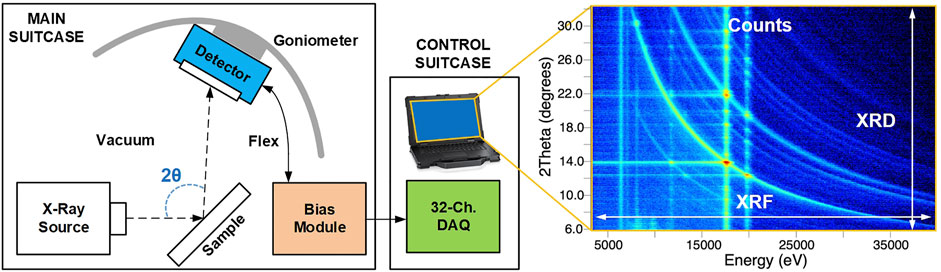
FIGURE 1. Concept of the transportable instrument here proposed for combined XRF-XRD analysis of samples in the field, for instance for mining applications. Example of an Energy/Angle map of a CaCO3 + FeSO4 sample simultaneously measured with this instrument.
The architecture of the instrument is shown in Figure 1. Since it will be operated in harsh environments such as milling sites, it needs to be robust and reliable. The presence of the X-ray tube, along with power supply, shielding, vacuum system and goniometer motor, makes impossible to carry the system in a backpack. The instrument instead can fit inside a vehicle and thus be transportable on land to the extraction site. The components are placed in two separate suitcases. Only the case containing the sample and radiation is in moderate vacuum (10 mbar) and shielded in order to reduce the volume to be shielded and, thus, the total weight. The X-ray source (a Mo tube operated at 50 W power and with air cooling for transportability) and the detector are placed in the main case. A goniometer with a radius of 15 cm hosting the detection module will be mounted in a Bragg-Brentano configuration scanning an angle 2θ from 7° to 30°. The main unit also contains a bias board powering the detection module. The secondary case contains the electronic platform processing and acquiring the signals in parallel, and a rugged laptop computer controlling the gonimeter motor and running the fitting algorithms, based on database of rock materials.
The main figures of merit used to assess the performance of this instrument which led the design are energy resolution (for XRF), angular resolution (for XRD) and the total measurement time per sample. Only very preliminary examples of instruments combining the two techniques with the same detector have been reported in the literature. In the field of cultural heritage, for instance, an interesting solution combining angle scanning with energy-dispersive XRD (EDXRD) was realized with a commercial single-pixel Amptek SDD coupled to a slit collimator with a very limited field of view [6]. The most successful (and rugged) portable instrument combining XRF and XRD was Terra proposed by the company inXitu Inc. in 2008 and based on a development for NASA of a instrument for planetary exploration (the CheMin module of the Curiosity rover analysing samples on Mars) and later applied to art objects [7]. The detector is a custom CCD offering a good XRD resolution of 0.3° and a poor energy resolution of 250–300 eV. Better energy resolution was achieved by using commercial Si-PIN detectors by Amptek achieving 200 eV [8] and 165 eV [9] in setups which have not reached industrial maturity.
2 Module design
2.1 Silicon microstrip detectors
Two dedicated R&D batches of strip detectors were fabricated in Fondazione Bruno Kessler (FBK, Italy) to produce the sensors for this project. The sensors were made with FBK p-in-n technology by p implants on high-resistivity
In these batches, many different sensor designs were produced, varying: 1) the strip pitch (from 100 μm up to 800 μm), 2) the strip length (from 6 mm up to 10 mm), and 3) the number of strips per sensor (from 32 channels up to 128 channels per sensor). All strip sensors have a bias line surrounding the sensors active area, which can be used to bias the strips via the punch-through mechanism when they are not independently contacted. This bias line can also be used to identify defective devices. Outside the bias line, there is a guard-ring (GR) structure based on a first biased ring, which has the purpose to collect the noise current originated outside the sensor active area, and a series of floating guard rings.
At the end of the fabrication process, all sensors were tested using automatic probers. For each sensor, the I-V curve of each junction and the current of each single strip were measured. A wafer with 450 μm thickness fabricated with the gettering process was selected and cut. Three sensors were mounted for the functional testing: one sensor with 100 μm pitch and 6 mm length and two sensors with 200 μm pitch and 6 and 10 mm length. As an example the IV curve of the complete sensor (see Figure 2) and the current of each single strip (see Figure 3) for the sensor with 200 μm pitch and 6 mm length are reported.
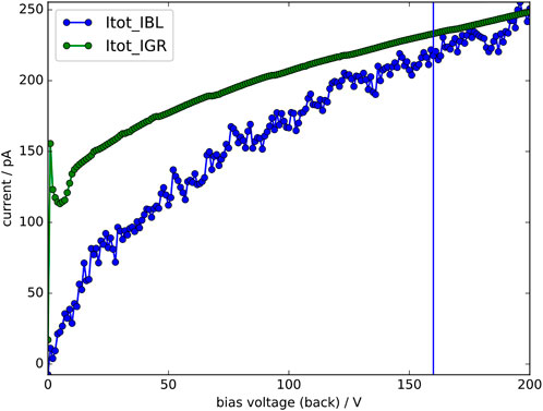
FIGURE 2. Example of the IV characterization of a complete sensors. The plot shows the current measured on the bias line (IBL, blue plot) and on the first biased guard ring (inner guard ring IGR, green plot) as a function of the bias voltage applied on the entrance window. The sensor is produced on a 450 μm thick wafer, with gettering process on the entrance window. The sensor has 32 DC-coupled strips plus 4 dummy strips at the borders, a strip pitch of 200 μm and a strip length of 6 mm.
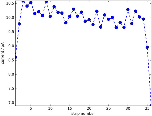
FIGURE 3. Example of the characterization of all single strips of a sensor. The plot shows the current measured on each strip at a fixed bias voltage of the entrance window (160 V). The sensor has 32 DC-coupled strips, a strip pitch of 200 μm and a strip length of 6 mm.
The IV curves of the other sensors showed a similar behaviour. The single strip current for the 100 μm pitch and of 6 mm length averaged to 4.6 pA. An image of the sensor mounted onto a dedicated ceramic board is shown in Figure 4). Naturally occurring reflections have highlighted in red and green two multi-channel preamlplifier ASICs and in blue the sensor itself. Above the ceramic board with the golden plated traces a spacer is visible. The details of the structure are explained in the dedicated section.
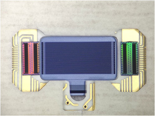
FIGURE 4. Photograph of the 32-channel strip detector with 100 μm pitch glued on top the PCB. Strips are wire bonded to the inputs of two CUBE front-end ASICs glued on the bottom of the PCB.
2.2 ASIC
An integrated front-end preamplifier was custom-designed for this application. The CUBE circuit was selected, being a charge preamplifier for the readout of silicon radiation detectors, in particular Silicon Drift Detectors (SDD), consolidated in spectroscopic applications [10] thanks to its low noise, equivalent to a few electrons, and its capability to reach high count rates (above 1 Mcps) [11]. The ASIC implements a charge integrator with pulsed reset. So far, the largest monolithic format of CUBE reported in the literature was a 4-channel version [12]. Here we present a 16-channel implementation targeting the operation with microstrips. The main challenge associated with increasing the number of channels regards cross-talk and the distribution of power supply on chip to the different channels. The channels pitch is 200 μm, matched with the pitch of the strips bonding pads. Two versions of the preamplifier were designed matching different detector capacitances: one optimized for the short strips (6 mm corresponding to 0.8 pF) and one for the long one (10 mm, 1.6 pF). The total ASIC area is 1 mm by 3.6 mm. Circuit simulations reported a noise of 176 eV (FWHM) with a detector capacitance of 1.5 pF, an operating temperature of −10°C, a 50 pA leakage current and an optimum triangular shaping time below 2 μs.
2.3 Assembly
The compactness of the detection module is important for its installation on the moving goniometer. A custom light- and air-tight package was developed. An exploded view of the package with all the components is shown in Figure 5.
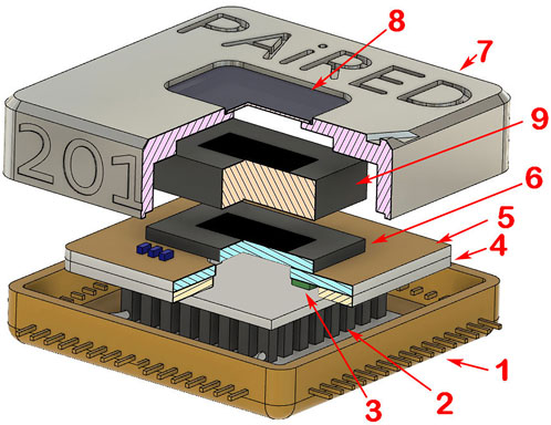
FIGURE 5. View of the detection module showing the main components of the assembly.
The final assembly is based on a commercially available QFN-64 package 1) of 2.6 cm side. The package is fitted with a thermoelectric cooling module 3) that allows stabilizing the sensors at low temperature, typically around -20°C. Inside the package, the silicon detector 6) is mounted on top of the PCB 5) - spacer 4) stack. Two 16-channel CUBE preamplifiers 3) are glued on the back side of the PCB, aligned to the sides of the detector and directly wire bonded directly to it. When required, a multi-layer silicon collimator 9) is added on top of the sensor. The collimator consists of a number of aligned silicon wafers with etched slits for every channel with width of the slits equal to half of the channel’s pitch. The cap of the package 7) is made of machined aluminum and has a aluminized 4 μm thick mylar window(8) that prevent light from reaching the sensor. Due to the large area of the window, the pressure inside the package is kept at 50 mbar of nitrogen. A photograph of the assembled module in shown in Figure 6.
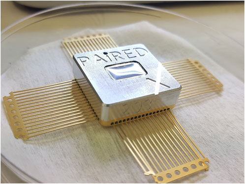
FIGURE 6. Photograph of the compact (2.6 cm side) packaged detector.
3 Materials and methods
A standard calibration 55Fe source was employed in all the tests here reported. The detection module was connected, by means of a flex cable (realized with single-layer flexible PCB) to a motherboard providing buffering, power supply, filtering, biasing and handling the reset of the preamplifiers. Data reported in the next section were acquired by means of a Digital Pulse Processor (DPP). In particular, a 32-channel DPP was realized by daisy-chaining four 8-channel DANTE DPP units (by XGLab, Italy), featuring 16-bit sampling at 62.5 Msps. The following operating modes were employed: 1) Waveform Acquisition: sampling of the input waveforms in oscilloscope mode to investigate signals and interferences in time domain and assess the leakage current of the detector; 2) FWHM Sweep: a parametric acquisition of spectra for different peaking times where the energy resolution is computed as FWHM of a Gaussian fit of the Mn Kα line at 5.9 keV. In this case a trapezoidal filter is applied and both peaking time and flat-top duration are selectable with 16 ns resolution; and 3) List Mode: recording each detected event with energy and timestamp, useful to study charge sharing among strips.
The choice of a bench-top DPP was motivated by the versatility offered by digital processing, required in the early phases of this development to optimize the detector operation. An OEM version of the DANTE DPP boards is available and was considered suitable for integration in the transportable instrument. However, if less bulky readout solutions would be required, an alternative approach based on Analog Pulse Processing (APP) could be adopted. Interestingly, APP was demonstrated to be equivalent to DPP in terms of energy resolution [13] up to count rates of about 1 Mcps per channel [14]. A 48-channel APP readout platform named Kerberos [15] was also used to readout the strip and a comparison in presented in Section 4.5.
4 Experimental results
4.1 Optimization of reference detector
The choice of the optimal geometry of the microstrips entails multiple compromises. The first trade-off concerns the pitch P: a small pitch enables better angular resolution for XRD, while it increases the charge sharing between adjacent strips, leading to an alteration of the spectrum. A second compromise is between energy resolution and sensitivity and it regards the strip length L. In fact, since the detector capacitance increases with L, the noise increases correspondingly, being detrimental for XRF. At the same time, reducing L implies a decrease of sensitive area and, thus, of the number of counted events (detrimental for both techniques in terms of statistics and measurement time). Based on these considerations, we chose as starting point of our investigation the detector with the shortest length (L = 6 mm) and largest pitch (p = 200 μm) since it is expected to present the best spectral performance.
First of all, the biasing voltage VHV of the strips was optimized. By keeping fixed the temperature and the shaping time, it was found that the energy resolution improves by increasing VHV up to reaching a plateau above 210 V. A value of 240 V was chosen and set in all the measurements (Figure 7A).
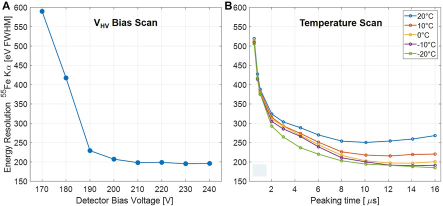
FIGURE 7. Premilinary optimization of the detector operating conditions: (A) strip bias voltage and (B) temperature.
Then the operating temperature was also chosen. As expected, by reducing the temperature the noise decreases and resolution improves. An operating temperature T between -10°C and -20°C is considered optimal, since it represents a trade-off between energy resolution and power dissipation of the cooling unit (Figure 7B).
Figure 8 shows the 32 spectra obtained in the optimal conditions (count rate of 2 kcps, peaking time of 14 µs, flat-top of 224 ns, T = -12°C), with an average energy resolution across the strips of 190 eV (FWHM at 5.9 keV) and very small standard deviation of 2.6 eV. In the following, this detector is experimentally compared with its geometrical variants (all DC-coupled) and performance are analyzed, in particular against these spectra taken as reference. The waveforms of the output signals from adjacent channels were analyzed and no visible cross-talk was measured.
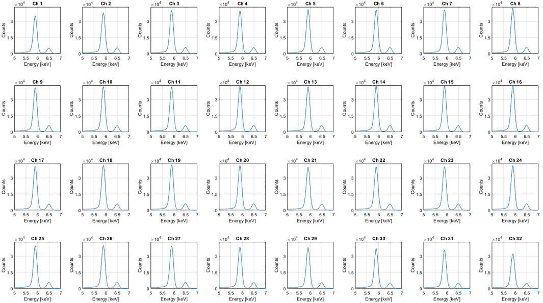
FIGURE 8. Spectra of an 55Fe calibration source acquired simultaneously from the 32 strips by means of Dante DPP at a rate of 2 kcps with a peaking time of 14 μs and detector temperature -12°C. The average energy resolution is 190 eV with a standard deviation of only 2.6 eV.
4.2 Strip length
When moving to a detector with the same pitch and longer L = 10 mm, the measured increase in the count rate (3.5 kpcs) is consistent with the increase of sensitive area. The two versions of the ASIC are compared and Figure 9 reports the comparison of the spectra measured in the same conditions. As expected, the longer strips are characterized by a larger noise, with an average resolution of 247 eV. This is consistent with the increase of capacitance, due to both a larger detector area and a larger matched input stage of the preamplifier. The bump between 2 and 4 μs in the sweep of peaking times is due to an interference observed when the flex cable connecting the module to the motherboard is not shielded. By wrapping and grounding an aluminum foil around the Kapton PCB, this interference is eliminated.
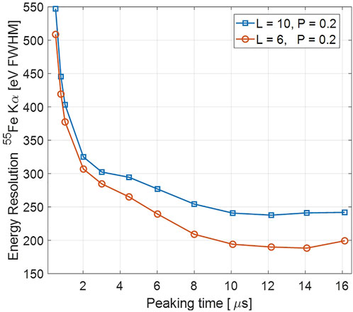
FIGURE 9. Comparison of detectors with different strip lengths (6 mm in orange and 10 mm in blue) in terms of energy resolution vs. peaking time. The lower noise of the shorter strip is evident.
4.3 Strip pitch
Then, detectors with the same L (6 mm) and different pitches were compared. By halving the pitch, the sensitive area halves too and this is experimentally confirmed by a decreased count rate of 0.9 kcps. Despite the decrease in the detector capacitance, the energy resolution does not change, as shown in Figure 10A. The average FWHM, measured with the same settings, is 209 eV. This worsening of the spectrum is due to an increased charge sharing between adjacent strips, as visible in Figure 10B. Charge sharing produces an increase of the low-energy tail due to partial collection of charge.
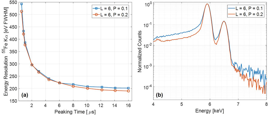
FIGURE 10. Comparison of detectors with different pitch (0.2 in orange and 0.1 mm in blue): (A) energy resolution vs. a sweep of peaking times and (B) spectra of 55Fe.
4.4 Impact of collimation and charge sharing analysis
In order to address the distortion of the spectrum due to charge sharing (CS), two strategies can be adopted: 1) physical collimation by means of a silicon collimator placed on top of the detector, or 2) electronic collimation by means of timing information. Both approaches improve the quality of the spectrum at the expenses of statistics. Both approaches were tested experimentally. In particular, the DPP was operated in list mode to acquire the timestamp of each detected event and signals from adjacent strips were analyzed. A charge sharing event is characterized by a splitting of the charge generated by the absorbed photon between two adjacent strips and is identified by a temporal coincidence window. When using photons of known average energy at an emission line (5.9 keV) it is found that events collected by adjacent strips within a time window of 56 ns are characterized by individual charges whose sum matches the total energy of the impinging photon. Different time windows and different energies were probed: the probability distribution of CS events (a Gaussian with a mean of 2.95 keV, i.e. 50% of the 5.9 keV peak energy, and standard deviation of 1.1 keV) was found to be energy-independent and taking place only between adjacent strips. By dividing the number of CS events with respect to the total number of collected events, it is possible to estimate the spatial extension of the CS region at the boundary between the strips, which resulted equal to 7 nm. Once CS events are identified, it is possible to exclude them from the spectrum. The Peak-to-Background Ratio (PBR) is used as figure of merit to assess the improvement of collimation. PBR is here computed as the ratio of counts in the 5.9 keV peak with respect to the background in an energy window of 400 eV around 3 keV. As reported in the spectra of Figure 11, when removing CS events the energy resolution does not change, but the PBR improves from 83 to 290. If the spectrum is dominated by a single peak, it is also possible to sum the energy of two CS event, thus increasing the number of events in the peak. In this case the PBR slightly increases to 310 and the number of events in the peak increases of 7.5%. When the collimator is placed on the detector, the PBR further improves and reaches a value of 600. Both approaches have advantages and drawbacks. In the first realization of the instrument the physical collimator will be employed, being a more consolidated approach. Despite being built by means of micro-fabrication techniques allowing micrometric accuracy, it introduces larger dead area between the strips with respect to electronic collimator, but is allows to adopt a simpler readout electronics.
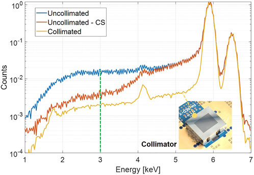
FIGURE 11. Impact of collimation, both physical and electronic, on acquired spectra (here normalized): uncollimated spectrum (blue), spectrum with removal of charge-sharing (CS) events detected with timing information (orange) and collimated one (yellow). The background is computed around the energy of 3 keV.
4.5 Comparison between DPP and APP
Finally, in order to demonstrate the feasibility of replacing the DPP with an APP based on miniaturized integrated shapers, we directly compared the two processing platforms with the same reference detector (L = 6 mm, p = 200 μm). We employed the Kerberos platform [15] mounting three integrated analog pulse processors named SFERA [16], each one containing sixteen 9th order semi-Gaussian shapers with programmable peaking time. Since the maximum peaking time of SFERA is equal to 6 µs, the average resolution across all strips is 270 eV FWHM. As show in Figure 12, when setting the DPP peaking time equal to 6 microseconds in order to have the same time occupation of the analog filter, the measured spectra are identical, confirming the equivalent resolution performance, here at count rates of 2 kcps. Figure 12 also reports all 32 spectra acquired with both platforms: the slight decrease in counts observed for the strips at the edges is consistent with the location of the source (placed at an height of 10 cm above the middle of the detector) and indicates that the illumination in not perfectly uniform.
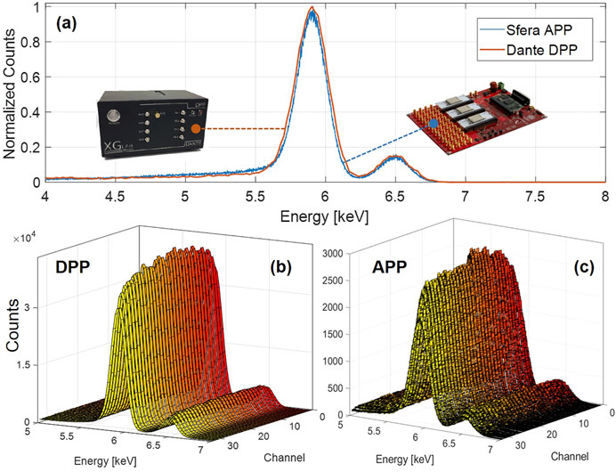
FIGURE 12. Comparison between DPP (Dante) and APP (Kerberos): simultaneous acquisition of the 32 channels with a filtering time of 6 µs, T = -12°C, L = 6 mm, p = 200 μm.
5 Conclusion
We have presented an extensive characterization of silicon strip detectors for simultaneous XRF and XRD measurements. The combination of two 16-channel integrated CUBE preamplifiers (developed for this application) with a careful design of the stack of boards and the thermo-mechanical assembly has allowed to achieve a very compact module. It can be mounted on the goniometer of the PAiRED-X project, as well as employed in other analytical portable applications. The result of the multiple experimental comparisons here reported is the identification of the optimal geometry (L = 6 mm, p = 0.2 mm) in terms of spectral quality (with an energy resolution for XRF below 200 eV with a peaking time of 14 μs). Longer strips increase the statistics of counts (of 66% moving to L = 10 mm), at the price of increased noise (increased of 30%) due to larger detector capacitance. With a pitch of 0.2 mm the angular resolution for XRD is about 0.07°, in line with the state of the art of 0.05° [8] and significantly better than the 0.3° achieved by the transportable Terra instrument [7] of similar use and scope of our prototype. A smaller pitch would increase the angular resolution, at the price of increased CS. CS can be reduced by means of physical collimation (thus increasing the PBR from 83 to 600, but halving the counts) or electronic collimation, which requires waveform digitization and thus is not compatible with APP. We have thus realized a single detection module for simultaneous XRD/XRF offering state-of-the-art performance in both analytical modes, with no penalty. From the point of view of energy resolution, we have also demonstrated, here with this type of detectors, that APP provides comparable performance to DPP (here for count rates of kcps), thus representing a viable alternative to miniaturize even more the instrument [13].
Data availability statement
The raw data supporting the conclusion of this article will be made available by the authors, without undue reservation.
Author contributions
Detector design and simulation (GB, NZ, GP), detector fabrication (GB, GP, FF, SR, and MCR), detector characterization (GB, MG, MC, ED, EB), assembly and electronics development (MC, MG, ED), paper writing (MC, GB, GP, CF), project supervision (MC, GP, LL, CF).
Funding
This research activity was supported by EIT Raw Materials under the project PAiRED-X.
Acknowledgments
We would like to thank Sergio Masci for wire bonding of the detectors and ASICs. Also, we acknowledge the contribution of Enrico Ferrara and Dr. Aidin Amirkhani, past students of Politecnico di Milano, in the early stages of the project.
Conflict of interest
The authors declare that the research was conducted in the absence of any commercial or financial relationships that could be construed as a potential conflict of interest.
Publisher’s note
All claims expressed in this article are solely those of the authors and do not necessarily represent those of their affiliated organizations, or those of the publisher, the editors and the reviewers. Any product that may be evaluated in this article, or claim that may be made by its manufacturer, is not guaranteed or endorsed by the publisher.
References
1. Gianoncelli A, Castaing J, Ortega L, Dooryhee E, Salomon J, Walter P, et al. A portable instrument for in situ determination of the chemical and phase compositions of cultural heritage objects. Xray Spectrom (2008) 37:418–23. doi:10.1002/xrs.1025
2. Uda M, Ishizaki A, Satoh R, Okada K, Nakajima Y, Yamashita D, et al. Portable x-ray diffractometer equipped with xrf for archaeometry. Nucl Instr Methods Phys Res Section B: Beam Interactions Mater Atoms (2005) 239:77–84. doi:10.1016/j.nimb.2005.06.214
3. Loubser M, Verryn S. Combining xrf and xrd analyses and sample preparation to solve mineralogical problems. South Afr J Geology (2008) 111:229–38. doi:10.2113/gssajg.111.2-3.229
4. Bortolotti M, Lutterotti L, Pepponi G. Combining xrd and xrf analysis in one rietveld-like fitting. Powder Diffr (2017) 32:S225–30. doi:10.1017/s0885715617000276
5. Bortolotti M, Lutterotti L, Borovin E, Martorelli D. Combined xrd-xrf cluster analysis for automatic chemical and crystallographic surface mappings. Powder Diffr (2019) 34:S36–S41. doi:10.1017/s0885715619000216
6. Mendoza Cuevas A, Bernardini F, Gianoncelli A, Tuniz C. Energy dispersive x-ray diffraction and fluorescence portable system for cultural heritage applications. Xray Spectrom (2015) 44:105–15. doi:10.1002/xrs.2585
7. Sarrazin P, Chiari G, Gailhanou M. A portable non-invasive xrd-xrf instrument for the study of art objects. Adv X-ray Anal (2008) 52:175–86.
8. Piga G, Santos-Cubedo A, Brunetti A, Piccinini M, Malgosa A, Napolitano E, et al. A multi-technique approach by xrd, xrf, ft-ir to characterize the diagenesis of dinosaur bones from Spain. Palaeogeogr Palaeoclimatol Palaeoecol (2011) 310:92–107. doi:10.1016/j.palaeo.2011.05.018
9. Pifferi A, Campi G, Giacovazzo C, Gobbi E. A new portable xrd/xrf instrument for non-destructive analysis. Croatica Chemica Acta (2009) 82:449–54.
10. Miliucci M, Scordo A, Sirghi D, Amirkhani A, Baniahmad A, Bazzi M, et al. Silicon drift detectors system for high-precision light kaonic atoms spectroscopy. Meas Sci Technol (2021) 32:095501. doi:10.1088/1361-6501/abeea9
11. Utica G, Fabbrica E, Carminati M, Borghi G, Zorzi N, Ficorella F, et al. Ardesia-16: A 16-channel sdd-based spectrometer for energy dispersive x-ray fluorescence spectroscopy. J Instrum (2021) 16:P07057. doi:10.1088/1748-0221/16/07/p07057
12. Bellotti G, Butt A, Carminati M, Fiorini C, Bombelli L, Borghi G, et al. Ardesia detection module: A four-channel array of sdds for mcps x-ray spectroscopy in synchrotron radiation applications. IEEE Trans Nucl Sci (2018) 65:1355–64. doi:10.1109/tns.2018.2838673
13. Hafizh I, Carminati M, Fiorini C. Assessment of analog pulse processor performance for ultra high-rate x-ray spectroscopy. Nucl Instr Methods Phys Res Section A: Acc Spectrometers, Detectors Associated Equipment (2019) 945:162479. doi:10.1016/j.nima.2019.162479
14. Hafizh I, Carminati M, Fiorini C. Tera: Throughput-enhanced readout asic for high-rate energy-dispersive x-ray detection. IEEE Trans Nucl Sci (2020) 67:1746–59. doi:10.1109/tns.2020.3001459
15. King P, Gugiatti M, Carminati M, Buonanno L, Borghi G, Pepponi G, et al. Design and characterization of kerberos: A 48-channel analog pulse processing and data acquisition platform. J Instrum (2021) 16:T07007. doi:10.1088/1748-0221/16/07/t07007
Keywords: X-ray fluorescence spectroscopy, X-ray diffractometry, silicon strip detector, integrated charge preamplifier, charge sharing
Citation: Carminati M, Borghi G, Demenev E, Gugiatti M, Pepponi G, Crivellari M, Ficorella F, Ronchin S, Zorzi N, Borovin E, Lutterotti L and Fiorini C (2022) 32-Channel silicon strip detection module for combined X-ray fluorescence spectroscopy and X-ray diffractometry analysis. Front. Phys. 10:910089. doi: 10.3389/fphy.2022.910089
Received: 31 March 2022; Accepted: 08 August 2022;
Published: 01 September 2022.
Edited by:
Ralf Hendrik Menk, Elettra Sincrotrone Trieste, ItalyCopyright © 2022 Carminati, Borghi, Demenev, Gugiatti, Pepponi, Crivellari, Ficorella, Ronchin, Zorzi, Borovin, Lutterotti and Fiorini. This is an open-access article distributed under the terms of the Creative Commons Attribution License (CC BY). The use, distribution or reproduction in other forums is permitted, provided the original author(s) and the copyright owner(s) are credited and that the original publication in this journal is cited, in accordance with accepted academic practice. No use, distribution or reproduction is permitted which does not comply with these terms.
*Correspondence: Marco Carminati, bWFyY28xLmNhcm1pbmF0aUBwb2xpbWkuaXQ=