 Gian-Franco Dalla Betta
 Marco Povoli
- 1Trento Institute for Fundamental Physics and Applications (TIFPA), INFN, Trento, Italy
- 2Department of Industrial Engineering, University of Trento, Trento, Italy
- 3SINTEF Digital, Oslo, Norway
In the past few years, there has been an increasing interest toward 3D silicon radiation detectors. Owing to their unique architecture, 3D detectors provide a remarkable radiation hardness at relatively low bias voltage (hence low power dissipation), that makes them the most appealing solution for use in the innermost layers of tracking detectors in High Energy Physics (HEP) experiments. Besides this primary application, the use of 3D sensor technology has been extended also to other fields, like thermal neutron detection and microdosimetry for proton and ion therapy. In this paper, we will review the state of the art and on going efforts in 3D detectors, covering the main design and technological issues, as well as selected results from the experimental characterization and TCAD simulation.
1 Introduction
Twenty-five years ago, the introduction of architectures with three-dimensional electrodes by Sherwood Parker and collaborators represented one of the most important advancements in silicon radiation detectors [1]. Differently from planar sensors, where the electrodes are confined to the wafer surfaces, 3D detectors consist of an array of columnar electrodes of both doping types, oriented perpendicularly to the wafer surface and penetrating deep into the substrate. This unique structure enables to decouple the active sensor thickness from the inter-electrode distance. The latter depends on the layout and can be made small enough to offer several important advantages with respect to planar sensors, among them lower depletion voltage (hence lower power dissipation), faster time response, and higher radiation tolerance, at the expense of a more complex fabrication process, which is based on a combination of microelectronics and MEMS technologies [2].
The superior radiation hardness of 3D detectors has been so far the main motivation for their development, aimed at High Energy Physics (HEP) experiments. In the earlier R&D phase (1997-2006), the feasibility of 3D sensors with good performance was proved on a few prototypes made at the Stanford Nanofabrication Facility (SNF) [3–6], also introducing the active edge concept [7]. These so-called Full 3D sensors from SNF were fabricated with a single-sided approach: column etching is performed all through the substrate from the front side of the sensor wafer for both types of electrodes, which are completely filled with poly-silicon, whereas the bottom side is oxide bonded to a handle wafer [3].
Later (2007-2010), the transfer of the Full 3D technology from SNF to SINTEF [8] and most of all the availability of the first prototypes of double-sided 3D sensors, independently developed by the Instituto de Microelectrónica de Barcelona (IMB-CNM, CSIC), that will be referred to as CNM [9] and Fondazione Bruno Kessler of Trento, Italy (FBK) [10], made it possible to proceed with more systematic studies [11, 12]. In fact, the double-sided approach, where junction (readout) columns are etched from one side, and ohmic (bias) columns from the opposite side, without the presence of a handle wafer, is intrinsically simpler and allows for shorter processing times, so that larger sets of samples became available and a wider community could be involved in testing activities.
A fundamental boost to 3D sensor development came from the 3D ATLAS R&D Collaboration, within which the four processing facilities (SNF, SINTEF, CNM, and FBK) pursued a joint effort aimed at one common design and compatible fabrication strategy for the production of 3D sensors for the ATLAS pixel Insertable B-Layer (IBL) [13]. 3D sensors with 50 μm × 250 μm pixel size, compatible with the FE-I4 readout chip were fabricated and successfully tested, showing to fulfill the IBL specifications: in particular, an in-time hit efficiency
At the end of this flourishing phase 3D pixels were produced at CNM and FBK and successfully installed in the IBL, their first HEP application [15]. Besides confirming the remarkable performance of 3D sensors, this milestone demonstrated the feasibility of medium volume productions with a relatively good yield, paving the way to using 3D pixels in other experiments (e.g., the AFP [16] and CT-PPS [17]), and also making them the most appealing option for the innermost layers of tracking detectors for Phase 2 upgrades at the High Luminosity LHC (HL-LHC). The latter application has in fact driven the most recent developments, leading to the advent of a new generation of 3D pixels with small pitch (25 μm × 100 μm and 50 μm × 50 μm) and reduced active thickness (∼ 150 μm) [18]. In parallel, other layout variants using trenched electrodes in place of columns, so as to achieve a more uniform electric field and weighting field distribution within the active volume, have been recently demonstrated to yield excellent timing performance, as requested by future HEP experiments to obtain a high 4D resolution (tracking + timing) [19].
The maturity of the 3D sensor technology has allowed for its use outside the HEP field. Interesting applications are in the detection of thermal neutrons through modified 3D structures filled with neutron converters, as well as in microdosimetry for proton and ion therapy, where cylindrical 3D structures are the basic sensitive elements of a new type of silicon microdosimeter.
In this paper, we will review the state of the art and on going efforts in 3D detectors, covering the main design and technological issues, as well as selected results from the experimental characterization and TCAD simulation. Section 2 reports on 3D sensors for HEP, Section 3 is devoted to 3D sensors for microdosimetry, and Section 4 to 3D sensors for neutron detection. Conclusions follow.
2 3D Silicon Pixels for HEP
2.1 Requirements for Phase 2 Upgrades
In view of the requirements of Phase 2 upgrades at HL-LHC in terms of increased radiation hardness, 3D sensors from the IBL generation fabricated at CNM and FBK were tested up to very large fluences with promising results [20, 21]. These studies were mainly carried out using 3D strip sensors, that do not need bump bonding and so can be irradiated separately from the read-out chip. A very high charge collection efficiency (CCE) was measured on CNM sensors with a basic 3D cell of 80 μm × 80 μm and an inter-electrode distance of ≃ 56 μm irradiated with 25 MeV protons at 2 × 10¹⁶neqcm−2. At 200 V reverse bias, the CCE is 27%, and it increases almost linearly with bias, also boosted by charge multiplication effects, up to ∼70% at 425 V, the maximum applicable voltage before breakdown [20]. In comparison, sensors from FBK with the same geometry, irradiated with 25 MeV protons at 2 × 10¹⁶neqcm−2, show a CCE of 27% already at 150 V reverse bias, but are then limited to ∼40% at 200 V by sharp breakdown [21]. The different characteristics of CNM and FBK sensors are justified by their different structural details, and particularly by the column depths: passing-through columns in FBK sensors [22] give a higher CCE at lower voltage compared to non-passing-through columns in CNM sensors [23], but surface breakdown effects prevent from being operated at very large voltages, so that charge multiplication effects can not be fully exploited [24].
In spite of the remarkable performance of IBL-like 3D sensors, the upgrades of the major experiments (ATLAS and CMS) at the HL-LHC called for additional improvements. In fact, besides radiation hardness, new sensors will have to cope with a very high event pile-up, up to 200 events per bunch crossing. In order to keep the occupancy at the
2.2 Sensor Design and Technology
From these requirements the design criteria of new 3D sensors and the implications for their fabrication process were derived. In 3D sensors, small pixel sizes naturally lead to small inter-electrode distances, comparable with the average carrier drift length due to charge trapping at the maximum considered fluences, so as to ensure high radiation tolerance [26]. Moreover, with small pixel size, the sensor active thickness should be decreased, for several concurrent reasons: 1) it limits the cluster dimensions, yielding a higher spatial resolution; 2) it helps reducing the overall material budget; 3) it reduces the electrode capacitance, hence the noise; 4) it allows for narrower electrodes, assuming the column aspect ratio (depth to diameter) attainable by Deep Reactive Ion Etching (DRIE) to be constant. Since the electrodes are dead regions, this latter aspect is essential to improve the geometrical efficiency; moreover, it further reduces the capacitance, and gives additional flexibility in the layout. However, thinner active regions also involve some disadvantages: the signals are obviously smaller, so the optimal thickness should be fixed taking into account the minimum requirements in terms of threshold set by the readout circuit; moreover, due to mechanical fragility and high bowing, a minimum wafer thickness is required both for fabrication and for bump bonding. In fact, high bowing would mainly impact on the accuracy of lithographical alignment, which is a common requirement for device fabrication and Under Bump Metallization in the bump bonding process.
At the beginning of the R&D for Phase 2 upgrades, CNM processed small-pitch 3D pixels on 4” diameter, 230 μm thick Float Zone wafers (i.e., the same substrates used for the IBL production) using an enhanced version of the double-sided technology, with narrower columns (≃ 8 μm nominal diameter) [27]. The double-sided approach is in fact well established and it provides several advantages in terms of reduced process complexity, shorter fabrication time, and ease of sensor assembly within a detector system, mainly due to the absence of the support wafer. Moreover, both sides of the wafer are patterned, so that the front side layout is less dense, that is convenient for small-pitch devices. However, it is not easy to process a wafer thinner than 200 μm without a support wafer, and the limited accuracy
FBK upgraded its fabrication line to 6″ diameter wafers in 2013. Processing wafers of 6” diameter with a thickness of less than 200 μm was deemed too risky for mechanical fragility considerations. Therefore, in the framework of a joint R&D program with INFN, FBK has developed a single-sided 3D technology with handle wafer, pioneering the use of Silicon-Silicon Direct Wafer Bonded (Si-Si DWB) substrates, where a Float Zone layer of the desired thickness and resistivity is directly bonded (i.e., without an oxide layer in between) to a thick low-resistivity handle wafer [18, 29].
Figure 1 (left) shows a schematic cross-section of a 3D pixel made on Si-Si DWB substrates with FBK technology. The p+ (ohmic) columns are etched deep enough to reach the p++ handle wafer, so that a good ohmic contact is achieved, which allows for back-side sensor bias. The handle wafer can be eventually thinned with a post processing and a metal layer can be deposited to ease wire bonding. In order to prevent from early breakdown [30], the n+ (junction) columns are etched stopping at a short distance (∼20 μm) from the p++ handle wafer. Both column types are partially filled with poly-Silicon, which also extends laterally at the column opening (poly-cap). A p-spray layer (not shown in the figure) is implanted on the front side to prevent the inversion of the surface and ensure isolation of the n+ columns.
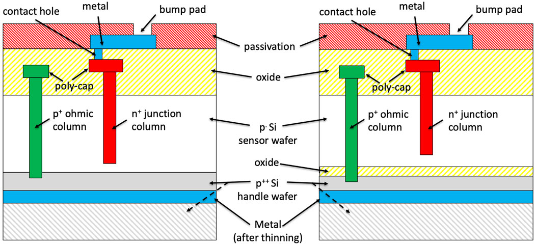
FIGURE 1. Schematic cross-sections of small-pitch, thin 3D pixels made at FBK with a single-sided approach on: SiSi DWB substrate (left), and SOI substrate (right). Not to scale.
FBK also demonstrated the feasibility of this technology with SOI wafers, proving that the p+ columns can be etched by DRIE through the buried oxide, so as to reach the p++ handle wafer [29] for back-side bias. While this solution is more demanding for the DRIE step, it should be noted that SOI wafers are compatible with passing-through columns, like in the original SNF process [3]. The device cross-section is shown in Figure 1 (right). In this case, a p-spray layer is also present at the back-side of the high-resistivity layer. While not strictly necessary for isolation in case of non-passing-through n+ columns, this prevents from having high electric field peaks at the interface close to the p+ columns, that would otherwise be induced by the increased concentration of electrons in the inversion layer caused by the build up of positive charge in the buried oxide after irradiation.
The non-participation to the production phase for the IBL has delayed 3D sensor developments at SINTEF, that reprised in collaboration with the Universities of Oslo and Bergen (Norway) in view of the Phase 2 upgrades. The fabrication yield problems affecting the IBL qualification batches were understood, and FE-I4 pixel assemblies were characterized in a beam test showing to be fully efficient at low voltage before irradiation [31]. Later, SINTEF fabricated new batches of sensors on 6″- diameter wafers using both Si-Si DWB and SOI wafers of active thickness ranging from 50 to 150 μm [32].
The FBK pixel layouts for the different geometries of interest for the ATLAS and CMS upgrades at the HL-LHC are shown in Figure 2. The 50 μm × 50 μm pixel (Figure 2A) has the simplest layout, since it matches exactly the same footprint for the bump bonding pads of the Readout Chip (ROC). There are one readout electrode (5 μm nominal diameter) at the center of a cell (50 × 50-1E) and four ohmic electrodes (6 μm nominal diameter) at the corners. The bump bonding pad has a non-negligible size (12-μm diameter in the passivation opening), but it can be easily placed on any side of the readout column. The inter-electrode distance (L) is ≃35.4 μm, small enough to ensure a high radiation tolerance.
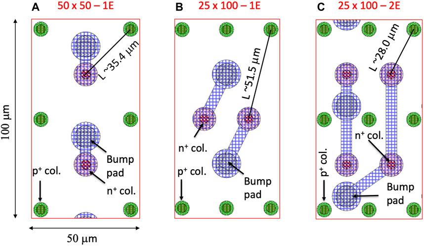
FIGURE 2. Layouts of two adjacent small-pitch 3D pixels of different geometry for the ATLAS and CMS upgrades at HL-LHC: 50 μm × 50 μm-1E (A), 25 μm × 100 μm-1E (B) and 25 μm × 100 μm-2E (C).
For the 25 μm × 100 μm pixel two design variants have been considered, having either one (25 × 100-1E, see Figure 2B) or two (25 × 100-2E, see Figure 2C) readout electrodes. In the 25 × 100-1E pixel, the layout is quite simple; the only complication derives from the need to place the bump bonding pads on a 50 μm × 50 μm grid compatible with the footprint of the ROC, which leads to an asymmetry between even and odd pixel rows. This layout has L ≃ 51.5 μm, a value that was initially believed to be not sufficiently small for radiation hardness, but it was later demonstrated to be good enough, as will be shown in the following. This motivated the choice to develop also a more radiation tolerant solution, the 25 × 100-2E pixel, with L ≃ 28.0 μm. However, this would come at the expense of a higher capacitance, which scales with the number of electrodes, and most of all it would be critical to manufacture. In fact, it can be seen in Figure 2C that the layout is very dense, and the bump pad is very close to the poly-Si cap of bias columns, that can lead to early breakdown in case of misalignment. This critical feature was the initial motivation for FBK to use stepper lithography in place of mask aligner, and lead to a sufficiently good yield of ∼40% [33]. Nevertheless, the 25 × 100-2E layout was eventually dropped by the ATLAS Collaboration because FBK was the only foundry available for its production.
2.3 Results
Since the RD53A chip became available only in 2018, the earlier prototypes of small-pitch 3D sensors from CNM and FBK had to be tested using existing ROCs from the previous generation, which feature larger pixels, e.g., 50 μm × 250 μm (FE-I4) and 150 μm × 100 μm (PSI46dig). To make the designs compatible, columnar electrodes were placed on either 25 μm × 100 μm or 50 μm × 50 μm grids corresponding to the small-pitch elementary 3D cells; one or more readout columns were then connected to the bonding pads of the ROC, while all the remaining n columns were shorted by a metal grid connected to the extra bonding-pads at the periphery (normally used for guard rings in planar sensors) that are grounded in the ROC [29]. This interconnection scheme provides some advantages: as many small pitch pixels as possible can be tested while ensuring proper boundary conditions (all columns are uniformly biased), and keeping the ROC tuning simple, since all read-out channels have the same input capacitance. The drawback is that most of the sensor volume is not active, making data analysis more difficult due to incomplete clusters.
The first CNM small-pitch 3D pixels were made with a Double-Sided (DS) technology and a layout compatible with the FE-I4 ROC [27]. They had a low mechanical yield and early breakdown (from 15 to 40 V) before irradiation, but good charge collection properties. They were tested at the CERN SPS H6 beam line with 120 GeV/c pions, showing a hit efficiency of 98–99% already at 1–2 V with perpendicular incidence beam (worst case, due to the very high electrode inefficiency) [34, 35]. After irradiation up to almost 3 × 10¹⁶neqcm−2, 50 μm × 50 μm pixels have shown to reach a hit efficiency of 98% with very high charge collection [35]: notably, only ∼100 V are required to reach the target hit efficiency of 97% at 1.4 × 10¹⁶neqcm−2 and even at 2.8 × 10¹⁶neqcm−2 the necessary voltage is ∼150 V. Correspondingly, the power consumption is remarkably low, with a value of only 13 mW/cm2 at -25 °C after 1.4 × 10¹⁶neqcm−2 [35].
The first study of a true small-pitch 3D assembly was carried out using CNM double-sided 50 μm × 50 μm pixels bump bonded to the ROC4SENS R4S chip [36]. Results from a beam test at DESY with 5.6 GeV electrons on non irradiated modules biased at 25 V show a hit efficiency of almost 99% for perpendicular particle tracks and larger than 99.5% already at 5° tilt, with a position resolution between 3 and 4 μm at optimal incidence angle of about 11°.
The first FBK small-pitch 3D pixels were made with a Single-Sided (SS) technology on Si-Si DWB substrates of 100 and 130 μm active thickness, and with a layout compatible with the FE-I4 and PSI46dig ROCs [29]. The electrical characterization of test structures have shown capacitance of the order of 50 fF per column, leakage current of only ∼ 1 pA per column, and intrinsic breakdown voltage higher than 150 V, in good agreement with TCAD simulations [37]. Pixel sensors were electrically tested on an automatic probe station, making use of a temporary metal. This method was originally developed at FBK for the IBL pixels [13, 22]. A temporary layer of metal is deposited over the passivation and patterned in strips; each strip contacts many pixels through the bump pad openings, shorting them to a common probe pad, where the currents are measured. The total current of a sensor is then obtained by summing all the strip currents. After the measurement, the temporary metal is removed.
The best wafers underwent bump bonding at Leonardo (Rome) and IZM (Berlin), and several pixel modules were tested in laboratory and in beam tests at CERN and Fermilab. Before irradiation, results were as expected, with relatively low noise figures (∼ 100 e− rms, compatible with the pixel capacitance), and hit efficiency higher than 99% already at low voltage [38]. Pixel modules of 50 μm × 50 μm assembled with FE-I4 ROCs were non uniformly irradiated at CERN IRRAD up to
FBK 3D pixel modules of different small-pitch geometries assembled with PSI46dig ROCs were measured in a beam test at Fermilab. The trend of collected charge versus bias voltage was shown to be compatible with the active thickness, and the overall efficiency was larger than 99% for perpendicularly impinging particles [38, 39].
Since 2018, most efforts have been devoted to the characterization of 3D pixel assemblies based on the RD53A chip, focusing the attention on the 50 × 50-1E and 25 × 100-1E. Results from the first CNM sensors made with a single-sided technology on SOI substrates of 150 μm active thickness are reported in [40]. Small-pitch pixels of both geometries were tested. Before irradiation sensors had early breakdown, but after irradiation with protons at 5 × 10¹⁵neqcm−2 they could be safely operated up to ∼170 V at -25°C. Results from a beam test at CERN with 120 GeV/c pions have shown a hit efficiency larger than 97% even without bias before irradiation, and larger than 96% already at 40 V after irradiation for perpendicular particles. By tilting the modules by 15°, the hit efficiency was obviously larger and saturated beyond 99% both before and after irradiation. Notably, the power consumption for 97% hit efficiency after 5 × 10¹⁵neqcm−2 was below 1 mW/cm2 at -25°C and 50 V bias [40].
Small-pitch 3D sensors from CNM were later irradiated up to 1 × 10¹⁶neqcm−2 and tested in DESY with electrons of ∼ 5 GeV energy [41]: at a bias voltage of 100 V, a hit efficiency larger than 97% with perpendicular incident particles was achieved for both designs; for the 25 × 100-1E, the hit efficiency further increased to more than 99% at 150 V with 15° tilt. The power consumption was below 10 mW/cm2 at −25°C and 150 V bias [41].
Similar results were obtained from beam tests of the first RD53A assemblies of FBK small-pitch sensors made on Si-Si DWB and SOI substrates of 130 μm active thickness [42, 43]. Before irradiation, the hit efficiency exceeded 98.5% for perpendicular incident tracks already at a bias voltage
Results for RD53A-based assemblies of 50 × 50-1E 3D pixels made at SINTEF on Si-Si DWB substrates of 50 and 100 μm active thickness and tested at DESY with 4 GeV electrons are reported in [46]. Before irradiation the hit efficiency was larger than 98.5% already at 2.5 V bias for both active thicknesses, also for perpendicular incidence particles. After irradiation, the hit efficiency for normal beam incidence reaches 97% at 40 V at 5 × 10¹⁵neqcm−2 and 96.5% at 80 V at 1 × 10¹⁶neqcm−2 [46].
Table 1 summarizes the main results from beam tests of small-pitch 3D pixel sensors from different foundries after irradiation. It is worth noting that all assemblies based on the RD53A ROC with 3D sensors from all foundries cope with the ATLAS Inner Tracker (ITk) requirement of a minimum hit efficiency of 96% at perpendicular beam incidence (97% at a tilt angle of 13–16°) [32]. Further beam tests on modules irradiated at the maximum fluence expected for the ITk (
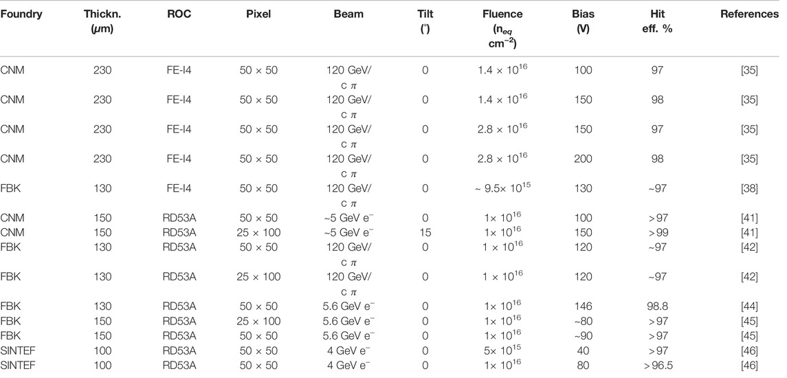
TABLE 1. Summary of the main results from beam tests of small-pitch 3D pixel sensors from different foundries after irradiation.
2.4 Ongoing Efforts
Based on the successful experience with the IBL, and on following results, the ATLAS experiment decided to equip the innermost layer (L0) of ITk with small-pitch 3D pixels of the two relevant geometries, i.e., 25 × 100-1E for the central barrel and 50 × 50-1E for the lateral rings. A comprehensive overview of 3D sensors for the ATLAS ITk has been recently reported in [32]. The ITk 3D sensor preproduction has been started at all processing facilities (CNM, FBK, and SINTEF). FBK sensors have already been delivered and cope with the specifications at wafer level. The first assemblies with the new ITKPix ROC are currently under test. Small-pitch 3D pixels are also considered for the upgrade of the CMS experiment at HL-LHC, and a final decision on their use for the innermost tracking layer will be taken soon.
Owing to their inherent radiation hardness, 3D sensors are also appealing for future experiments, e.g., the Future Circular Collider (FCC), where extreme fluences up to 8 × 10¹⁷neqcm−2 are expected [47].
Charge collection efficiency (signal efficiency) studies of heavily irradiated small-pitch 3D sensors (mainly strip and diodes in order not to be limited by the ROC limited tolerance) have already been reported. As an example, CNM sensors of 50 × 50-1E geometry have reached 90% (80%) signal efficiency at 175 V after 1 × 10¹⁶ (1.5 × 10¹⁶)neqcm−2 [48]. Moreover, a signal efficiency of up to 75% at 175 V after 1.7 × 10¹⁶neqcm−2 has been reported [49]. FBK 3D sensors of different small-pitch geometries were irradiated up to 3.5 × 10¹⁶neqcm−2 and tested with a position sensitive laser setup [50]: the signal efficiency for the 50 × 50-1E geometry at 175 V was 90% (80%) after 1 × 10¹⁶ (2 × 10¹⁶)neqcm−2, and even larger for the 25 × 100-2E geometry. These results are boosted by charge multiplication effects, which were previously observed in 3D sensors of larger pitch [20], but are now anticipated to lower voltages due to the smaller pitch of recent prototypes, in good agreement with TCAD simulations [51].
An interesting study was carried out on CNM sensors of 50 × 50-1E geometry, irradiated up to unprecedent fluences: at only 150 V bias, after 1 × 10¹⁷neqcm−2 the signal efficiency was found to be 20%, and still ∼15% after of 3 × 10¹⁷neqcm−2 [52].
Even better performance could be achieved by further downscaling the pixel sizes, so as to better control charge multiplication effects [53]. A preliminary study is reported in [54], where it was demonstrated the feasibility of 25 μm × 25 μm pixel cells in diode test structures at FBK. As an example, Figure 3 (left) shows a layout detail, whereas Figure 3 (center) and 3 (right) show the I-V and C-V characteristics, respectively. Normalizing the measured data to the number of columns (3,600) present in a 3D diode, the current at 30 V bias is ∼170 fA/column and the capacitance ∼75 fF/column, still good enough for a future pixel implementation. Charge collection tests with a beta source at the University of New Mexico have shown a moderate charge multiplication before irradiation with a gain of ≃2.3 at 70 V [54]. Further efforts on very small pitch 3D sensors are under way at FBK also taking benefit from the enhanced spatial resolution and alignment capabilities of stepper lithography [33].
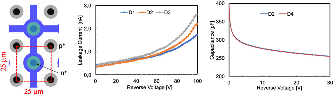
FIGURE 3. Layout detail (left), I-V curves (center), and C-V curves (right) of 3D diodes with 25 μm × 25 μm basic cell. Different device samples from the same wafer (D1, D2, D3, and D4) are indicated in the legends.
Other relatively recent R&D efforts have been devoted to the development of 3D sensor for tracking + timing applications, in view of experiments at future colliders where vertex detectors will require time information. Even though 3D sensors are intrinsically fast devices, for a long time the only study dealing with their timing properties was that of [55], where Sherwood Parker reported results from non-optimized test structures, with signal full width of ∼5 ns, rise time of ∼1.5 ns, and timing resolution from ∼ 30–180 ps, depending on the signal amplitude.
More recently, a 50 × 50-1E 3D single-pixel test structure made at CNM with a double-sided process on ∼285-μm thick substrate was tested with a fast discrete readout channel, showing a timing resolution of ∼30 ps at 150 V bias and −20°C with inclined particle tracks [56]. The same type of test structure was tested after irradiation up to 1 × 10¹⁶neqcm−2, showing a timing resolution lower than 50 ps at 150 V bias and −20°C [57]. This remarkable timing performance is however limited by the electric field and weighting field spatial non uniformities which are typical of 3D sensors [1, 55].
A possible solution to optimize the timing performance, that was already proposed in [55], consist in replacing columnar electrodes with trenched electrodes. Trenched electrodes were originally implemented at SNF as a precursor to active edges [7]. Later the BNL group, in collaboration with Stony Brook University, proposed a detector with a columnar electrode at the centre of a cell surrounded by hexagonal-shaped trenches, reporting some preliminary results from the characterization of the first large pitch (500 μm) prototypes fabricated at CNM [58]. Small-pitch 3D sensors with dashed-trenched-electrodes were fabricated at SINTEF and tested at the University of Trento with a position resolved laser system, showing good charge collection properties after irradiation up to 1 × 10¹⁶neqcm−2 [59]. However, none of these devices were intended for timing applications.
A dedicated R&D effort in this direction has been pursued within the INFN TIMESPOT project [19, 60–64]. The 3D-trenched pixel design has been carried out with the aid of TCAD simulations, also taking into account some relevant constraints for fabrication, that have been investigated by dedicated technological tests at FBK [60, 61]. A pixel size of 55 μm × 55 μm has been considered, in order to be compatible with the readout chips of the TIMEPIX family. Figure 4 shows the layout and photograph of a pixel. The pixel layout has been optimised aiming at the best trade-off between the intrinsic sensor response time, as derived from the uniformity of electric and weighting field distributions, and the capacitance, the latter affecting the bandwidth of the read-out channel and its noise, thus degrading the timing performance. The first batch of TIMESPOT sensors was produced at FBK in 2019 on Si-Si DWB substrates using a single-sided fabrication process [62]. From measurements at wafer level, sensors were found to be fully depleted at a few Volts, with a leakage current as low as ∼10 pA/pixel, and a breakdown voltage in the range of 150–200 V, which allows for a wide operational range. The capacitance was also measured and found to be ∼ 70-75 fF/pixel at full depletion, in good agreement with simulations.
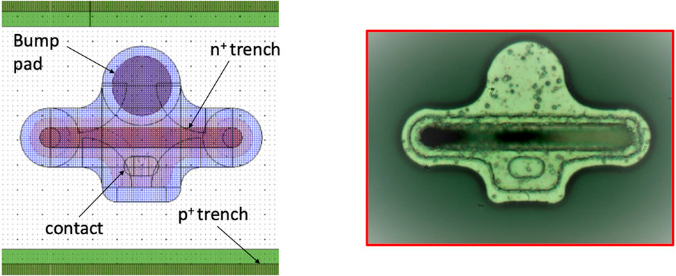
FIGURE 4. Layout detail (left) and photograph (right) of a 3D pixel with trenched electrodes of 55 μm × 55 μm size.
In a beam test at PSI with 270 MeV/c pions, an outstanding timing performance (
In order to take full benefit from the timing performance of the sensors, a dedicated ASIC, TIMESPOT1, with pixel level integrated TDC has been designed in 28 nm CMOS and is currently being tested, with promising results (∼30 ps on the ASIC alone) [65]. The first assemblies of TIMESPOT1 prototypes bump-bonded to 32 × 32 3D-trenched pixel sensors of 55 μm pitch have been realized and will be tested under a beam of particles in summer 2022.
3 3D Silicon Micro-Dosimeters
One of the first uses of the 3D sensor technology outside HEP is in solid-state microdosimetry for measurements of radiation doses in medical and aerospace applications.
The biological effects of radiation have a strong dependence on the pattern of the energy deposition at microscopic scale. Microdosimetry was developed to provide a description of the spatial and temporal distribution of the absorbed energy in irradiated matter [66]. The challenges posed by microdosimetry are related to tissue-equivalence, minimum size and shape of the sensing elements.
The most common microdosimetric device is the Tissue-Equivalent Proportional Counter (TEPC), a gas based detector with a spherical or cylindrical ionization chamber. The TEPC is typically considered tissue-equivalent because of the gas mixtures used [67, 68]. Although very popular, the TEPC has a number of shortcomings including large size, high voltage requirements and the inability of mimicking an array of cells. In recent years, attempts have been made to miniaturize the TEPC [69], but some of the issues identified remain unsolved.
In order to address the shortcoming of the TEPC, attempts have been made to use silicon based devices as microdosimeters since the early 1980s. Investigated devices included silicon diodes [70], commercial DRAM cells [71, 72], CCDs [73] and MOS transistors [74]. The main limitations identified were related to the poor definition of the sensitive elements, radiation hardness and lack of tissue equivalence.
Aiming at solving the issues with earlier silicon-based microdosimeters, the Centre for Medical Radiation Phyisics (CMRP) at the University of Wollongong, Australia, was the prime proponent of a new type of device based on SOI technology [75, 76]. This approach aimed at creating arrays of microscopic sensitive volumes that would mimic arrays of biological cells. Using SOI wafers allowed the thickness of the active layer to be reduced to just a few microns, while the advances in photolithography were able to deliver silicon cells of the size of a few tens of microns. The small size of the silicon sensitive volumes translates into low operating voltages, considerably reducing power consumption. Over the following years, several iteration of the SOI microdosimeter were proposed with excellent results [77–80].
The experience gained with SOI microdosimeters allowed to identify the main limitations that needed to be addressed in the following sensor generations. The investigated devices made use of planar processing to create the sensitive elements of the arrays by means of ion implantation. In addition, using SOI wafers meant that both n+ and p+ electrodes had to be fabricated on the same side of the detector. This resulted in sensitive volumes suffering from poor definition of the active volume, due to charge sharing between neighbouring cells, and charge collection from outside of the cells/arrays. In addition, the basic elements were fully built into the silicon material, resulting in poor tissue equivalence.
The use of 3D sensor technology in microdosimetry was proposed by A. Rosenfeld [81] to address the issues identified with the previous SOI approach. Exploiting the ability of 3D sensor technology to etch high aspect ratio structures into the silicon bulk, a fully enclosed cylindrical electrode can be created. This results in the complete isolation of a portion of the silicon substrate from the rest of the material, thus obtaining a perfectly defined sensitive cell that would not suffer from charge sharing or any charge collection from the outside. Improvements to the tissue equivalence of the sensor can be achieved by removing the inactive silicon outside of the sensitive volumes by means of DRIE, and by replacing it with polyimide or PMMA. A comparison between a planar and a 3D microdosimeter cell is shown in Figure 5.
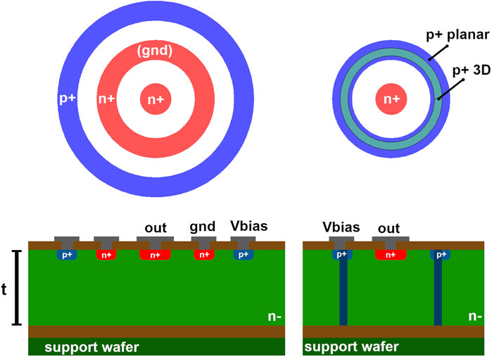
FIGURE 5. Comparison between the layouts and cross section of the basic cell of a planar (left) and 3D (right) microdosimeter.
The investigation in 3D microdosimeters started in 2013 in a collaboration between SINTEF and CMRP [82] funded by the Norwegian Council for Research. A similar approach was later pursued at CNM [83]. Over the years, several iterations of the technology were completed at SINTEF, each improving on the previous and refining the optimal design and shape of the basic elements. Figure 6 shows a detailed cross-section of 3D micro dosimeter cell, highlighting all of the elements discussed in the following paragraphs. 3D microdosimeters have been fabricated on SOI wafers with thin active layers (i.e., 2, 5, 10, 20 and 50 µm), but fabrication on Si-Si DWB wafers is also feasible. The interconnections between cells can be laid out in single cells, strips, or arrays/pixels, and different readout schemes can be implemented. The most important feature of a 3D microdosimeter, is that the basic sensitive elements constituting the arrays, should have efficient and uniform charge collection, within a well-defined volume, thus guaranteeing the accurate extraction of the microdosimetric quantities from the measured spectrum.
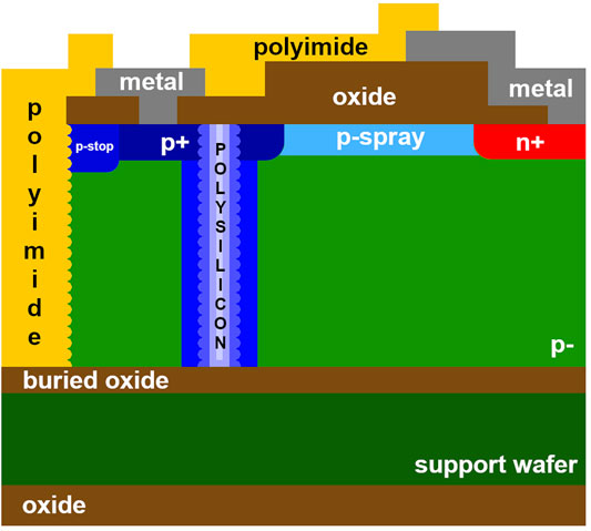
FIGURE 6. Complete radial cross-section of a sensitive volume fabricated with 3D technology.
After considerable efforts in functional testing with radiation beams [84], it was possible to draw several conclusions on the correct implementation of the basic sensitive volumes of a 3D microdosimeter: 1) the ideal ratio between cell diameter and cell thickness was found to be equal to 2 (e.g., d = 20 μm, t = 10 μm); 2) the walls of the cells should be created using a 3D trench electrode with a fully enclosed layout (a continuous circular trench); 3) the readout electrode in the middle of the cell should be planar and created with a shallow implantation to avoid the loss of charge collection efficiency associated with a 3D columnar electrode or a deep implanted layer.
3D microdosimeters are typically fabricated with an N-on-P approach (n+ planar electrode and p+ 3D wall electrode in a p-type substrate), to exploit the advantages in terms or radiation hardness and electron readout. The 3D structures are etched by DRIE, doped by gas diffusion and completely filled with polysilcon or other materials like Tetraethyl orthosilicate (TEOS) to restore the planarity of the silicon wafer. If the trench electrode is fully enclosed, p-spray/p-stop implants are not strictly necessary. It is however desirable to have both p-spray inside the cells, and p-stop everywhere outside of the cells under the metal lines. The necessity of a good interface passivation becomes evident when operating the sensors in high intensity heavy-ion medical beams. In these applications, the amount of charge released in silicon can be so large, that a non-negligible signal can be induced on the metal lines through a MOS effect across the oxide layer.
The tissue-equivalent polymer is integrated into the sensors at wafer level, after the devices have been characterised electrically. The active cells are covered with a photoresist layer to avoid damage during the removal of the outer inactive silicon by means of DRIE. This step produces free-standing sensitive volumes (“mushrooms”) connected by silicon bridges and metal lines. The space between the cells is then back-filled using a tissue-equivalent polymer. The choice of tissue-equivalent material depends on two main factors: 1) availability and compatibility with silicon processing; 2) feasibility of the deposition method. The material available at SINTEF was polyimide deposited by spin coating. Because of the properties of the material and the thickness of the required polyimide film, the procedure must be carried out in multiple steps. For example, for a 10 μm thick device layer, the polyimide is deposited in 4 steps with alternating vacuum and thermal treatment to remove trapped air bubbles. A photolithography to open the layer over the pads and in the dicing lanes is required every 5 μm of deposited polymer. The polymer is then imidized (hardened), forming a solid and strong layer encapsulating the sensitive volumes. It was discovered that depositing and patterning of a polyimide layers thicker than 10 μm can be challenging and a different procedure will need to be developed in the future.
The 3D-microdosimeter technology at SINTEF is now quite mature and reliable. Over the multiple sensor generations, critical aspects have been understood and addressed, and can be summarized as follows. The width of the 3D openings must be kept as small as possible to facilitate the restoration of the wafer planarity after back filling with polysilicon. A failure in doing so, will cause excess topography making the following processing steps challenging. In addition, excess topography of the trench electrodes can cause reliability issues with the metal lines crossing the trench to readout the core electrodes (broken connections). Wafer curvature was found to not be an issue, unless the active layer thickness exceeds 20 μm, at which point it has to be managed similarly to what is done for a full 3D detector processes. The integration of the tissue-equivalent polymer can be achieved easily up to thicknesses of 10 μm. For thicker layers, new techniques like spray-coating and different materials will have to be tested (options are currently under investigation at SINTEF). Producing 3D microdosimeters on Si-Si DWB wafers instead of SOI can provide considerable simplification of the layout of the metal interconnections, because the bias can be provided from the support wafer. This solution was tested successfully in the latest production run at SINTEF completed in late 2021. The sensors are currently being characterized at CMRP and results will be available shortly. The technology can be improved by further reducing the size of sensitive volumes, and increased alignment accuracy. Because of the limitations in alignment precision of standard mask-aligners, more advanced lithographic techniques should be used (e.g., mask-less lithography or stepper lithography).
4 3D Neutron Detectors
Another interesting use of 3D detector technology that has gained popularity in the past 2 decades, is the production of semiconductor-based neutron detectors for applications in homeland security, neutron science, neutron imaging and more [85]. Typical neutron detectors are gas-filled and Boron-lined proportional detectors, scintillators coupled to photodetectors and semiconductor detectors. The choice of detection methodology depends on the experimental requirements like energy of the neutrons and area coverage. While very popular, gas-based detectors make use of scarce gasses like 3He [86], or highly toxic gases like BF3 [87], and technologies that can achieve good detection efficiency without the use of these gasses, would be preferable.
Solid-state radiation detectors have attracted interest in the past decades in a large number of applications using different types of radiation. Their use is particularly interesting in neutron imaging applications using thermal neutrons, because of the advantages they can offer in terms of spatial and time resolution. Two different approaches to solid-state neutron detection are available: 1) neutron-sensitive semiconductor materials (e.g., LiINSe2, LiSe, BN) and 2) semiconductor sensors coated with thin films of neutron converter materials. While the first approach has the potential to deliver excellent detection efficiency because the neutrons are converted directly into the material, the control of the crystal quality and defects is challenging and often severely impacts the charge collection efficiency of the sensors. Coated semiconductor detectors are an easier choice, but their detection efficiency strongly relies on device geometry, converter layer thickness and choice of the converter material and, therefore, conversion products. The neutron converter material is chosen based on its neutron capture cross-section (higher values are better) and on the type conversion products. Good candidates for neutron converter materials are 10B, 6Li, 157Gd, 113Cd [88]. Gadolinium and Cadmium offer the largest cross-section, but their conversion products are mainly γ-rays, which are undesirable in neutron applications due to the difficulty in discriminating them from the background gamma radiation. Boron and Lithium are better candidates, despite having a smaller cross-section, because their conversion products are charged particles with ranges of roughly 2–33 μm.
Planar detectors coated with 10B and/or 6Li films were amongst the first semiconductor detectors to be tested for neutron applications. Calculated detection efficiencies were found to range between
Coated three-dimensional silicon neutron detectors were first proposed as an alternative to planar silicon detectors in the late 80s [91], and fully developed in the late 90s [92] with the intent of drastically improving the detection efficiency while retaining all the features of their planar predecessors. The idea was to create 3D micro structures on the detector surface, that would later be filled with neutron converting materials. This approach was expected to deliver enhanced efficiency because the effective converter thickness and surface area are decoupled from the ranges of the conversion products, resulting in high neutron absorption probability without affecting the detection of the reaction products. In addition, if the micro structures are designed correctly, conversion products generated in opposite direction can both be collected and γ-ray rejection can be enhanced. A schematic device concept is shown in Figure 7.
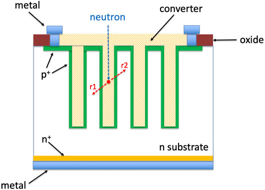
FIGURE 7. Schematic cross-section of a 3D (microperforated) neutron detectors (r1 and r2 are the reaction products).
Many research groups have been active in 3D neutron detector research in the past decade, exploiting modern silicon micro-machining techniques. A summary of the current state-of-the-art of 3D neutron detectors is given in the following subsections, with focus on the latest and most promising developments obtained in the past decade.
4.1 Kansas State University
Kansas State University has been one of the most active players in this field since it was introduced. Detailed MonteCarlo simulation studies were carried out with the intent to study and optimize different implementation of the 3D neutron detector concept. Examples can be found for single-sided perforated 3D detectors with micro-structures of different shapes (holes, pillars and trenches) [88], and dual-sided semiconductor detectors with similar cavity geometries [93]. Both 10B and 6Li in powder form were considered as converting material. The theoretical efficiencies obtained from simulations were over 35% for the single-sided approach and over 70% for the double-sided approach. Despite the promising results, the simulations only offer a picture of the sensor performance in absence of dead layers on the walls of the micro-strucures (e.g., oxides and/or doping layers), and do not account for inefficiencies in the collection of the carriers generated in the sensors. All these effects are expected to considerably degrade the theoretical neutron detection efficiency.
Single-sided detectors were fabricated using ICP (Inductively Coupled Plasma)-RIE (Reactive Ion Etching) and the cavities were passivated with silicon oxide or by dopant diffusion. The measured efficiency for fabricated single-sided detectors were as high as 16.2% for sinusoidal trenches [94].
One way to increase the detector efficiency is stacking multiple detectors with a well-defined pitch, so that the trenches of one detector would coincide with the non-etched silicon in the following detector. This strategy resulted in neutron detection efficiencies as high as 42% [95]. Double-sided detectors were found to achieve efficiencies similar to the stacked detector approach [96].
It is important to note that many of the described approaches were never intended for neutron imaging and could not directly be coupled with a readout chip for pixel detectors. A dedicated implementation of the single-sided approach compatible with the TimePix readout chip, was simulated in great detail with promising results, that should soon be confirmed with fabricated detectors [97].
After many years of research some of these detector implementations are being adopted in the field. For example, wearable detectors are being produced to aid in the search and localization of special nuclear materials [98], and compact neutron detector system for planetary exploration are being investigated [99].
4.2 Lawrence Livermore National Laboratory
The development of 3D neutron detectors at Lawrence Livermore National Laboratory started in 2005. The detector sensitive elements are p-i-n micro-pillars submerged in converter material (10B). The pillars can be fabricated by means of either micro-machining (DRIE) or by selective growth of nanowire pillars [100]. In order to achieve high neutron detection efficiency several parameters must be calibrated correctly. Different combinations of pillar diameter, height and pitch were simulated with promising neutron detection efficiency expected for small diameters/pitches
The starting material was a planar epitaxial P-I-N structure grown on an n+ silicon substrate. The pillars were defined by standard photolithography and etched using a ICP-DRIE process. The plasma-generated damage was removed by an isotropic wet etch in a nitric acid based solution followed by a deposition of silicon oxide to achieve passivation of the silicon wall [101]. An additional challenge was posed by the need for conformal deposition of the neutron converter. This was achieved with a dedicated Chemical Vapor Deposition (CVD) process [102]. After converter deposition, some of the material was etched back to allow for the deposition of the metal contacts on top of the pillars.
Excellent experimental results were reported with this detector geometry. Initial tests with pillars of 2 μm diameter, 4 μm pitch and 12 μm height, delivered relatively low efficiencies (∼7.3%). By increasing the height of the pillars to 26 and 50 μm, the efficiency was increased to 22% and 48.5%, respectively [101, 103]. More recent efforts were dedicated to the fabrication and characterisation of a compact and portable neutron multiplicity system [104]. Efficiencies as high as 35% were achieved.
Although no attempts at neutron imaging were made with these devices, the technology can be adapted to produce detectors compatible with the necessary pixel readout chips.
4.3 Rennselaer Polytechnic Institute
The development of solid-state neutron detectors at the Rensselaer Polytechnic Institute has seen remarkable results in the past decade. The proposed structure, though similar in approach, differs quite drastically from the ones previously described [105]. The detectors are fabricated on a low resistivity n-type wafer, on which two epitaxial layers are first deposited [106]. The first layer n-type, 50 μm thick, and lightly doped (50 Ωcm), acting as the sensitive volume of the sensor. The second layer is p-type, 1 μm thick, and highly doped (0.01 Ωcm) forming the p-n junction used as planar readout electrode. A matrix of staggered hexagonal holes was etched into the top layer to a depth of about 40 μm using DRIE masked with a stack of oxide and photoresist. After resist removal, the micro-structures were passivated in the same deposition step used for the boron-based neutron converter, performed with a dedicated Low Pressure CVD (LPCVD) process [107]. After removal of the silicon oxide used for masking of the deep etch, the process was completed by sputtering of Ti-Al metal contacts on both sensor sides. The electrical characterisation demonstrated the success of this approach, with low leakage currents confirming the correct passivation of the micro-structures. Sensors from the first technology iteration operated at very low bias, were tested under perpendicular neutron flux using a 252Cf source. The sensors showed a relatively low efficiency of about 4.5% [105], due to the fact that natural boron was used as converter. By replacing the natural boron converter with 10B, it was possible to achieve efficiencies of ∼26% [108]. It is important to note that this approach would be compatible with neutron imaging after some modification to the fabrication process to segment the p-n junctions and the readout electrodes. These devices were recently used to produce a modular directional and spectral neutron detection system [109]. Although more work is required to increase the overall efficiency of the full instrument, the results are promising.
4.4 University of Trento
Building on the large experience gained in 3D detector fabrication and characterization for HEP applications, the University of Trento in collaboration with FBK started developing 3D neutron detectors in the early 2010s. The first device concept (HYDE1) followed the philosophy of the earlier 3D-STC (3D Single Type Column) approach [110]. In this implementation, only one type of electrode is fabricated with the 3D architecture, in this case the n-type electrode (junction electrode). The cavities housing the neutron converter were etched on one side of a p-type FZ silicon wafer and doped by phosphorus gas diffusion. In this first prototype large cubic cavities were produced of side 200 μm. Planar electrodes, both n+ and p+, where created by ion implantation on the opposite side of the wafer. The cavities were contacted through the planar electrodes by means of small Through Silicon Vias (TSV) filled with polysilicon. Isolation between the different cavities was obtained by means of a p-spray implantation, while the planar n+ electrodes on the opposite side of the wafer were separated by the planar p+ electrodes (p-stop style). The detectors were readout as diodes with all the cavities shorted together by the metal layer on the planar side of the wafer. Thorough testing of the HYDE1 prototypes was carried out in laboratory and in neutron beams [111, 112]. The electrical characterization showed good leakage current of a few nA/cm2 [113]. The neutron tests were carried out after filling of the cavities with 6Li powder. An estimated efficiency of 4.12% was obtained at the Politecnico di Milano (Italy), using a moderated neutron source and a reverse bias of 10 V. This result was lower than the value predicted by GEANT4 simulations (11.86%) for primarily three reasons: 1) the density of the 6Li powder was much lower than the tabulated one, 2) the applied bias was too low to ensure fully efficient charge collection, and 3) the simulation did not account for the extension of the dead layers in the sensor. This approach is fully compatible with neutron imaging without modifications to the fabrication process, by ensuring that the single cavities fit in the size of one pixel (i.e.,
The second technology iteration, HYDE2, included both diodes and pixel detectors compatible with the Medipix2/Timepix readout chip. The sensor geometry was tailored to the use of boron-based neutron converters. This required a complete re-design on the 3D micro-structures but allowed to simplify the fabrication process. The etched structures were considerably smaller in size and pitch when compared to HYDE1 detectors. They were not doped and only passivated by a very thin layer of ALD Al2O3, in order to reduce the extension of the dead layers to a minimum. The use of ALD Al2O3 for passivation is only compatible with p-type silicon substrates and excellent results are reported in literature [114]. The micro-structures were arranged in arrays of different shapes designed with the help of GEANT4 simulations. The considered neutron converter was 10B with thickness of 1 μm. Simulation results demonstrated neutron detection efficiencies as high as 30% can be achieved for small structures (2–5 μm) with thin separating walls (1–2 μm) and etched to a depth of about 20–30 μm [85]. Initial tests showed excellent electrical properties, both in terms of low leakage current (∼ 5 nA/cm2)and high breakdown voltage (
4.5 Other Groups
Amongst the very first research groups working on solid-state neutron detectors, was the Czech Technical University (CTU) in Prague, investigating planar silicon diodes coated with 6LiF [116, 117]. More recent studies focused on the use of planar pixel detectors compatible with the Medipix/Timepix readout chips, for which spatial resolution better than 10 μm was demonstrated [118, 119].
The use of 3D technology was first investigated through the simulation of cylindrical and square pores filled with 6LiF and 10B, showing detection efficiencies as high as 32% [120]. A different approach to micro-structure detectors was proposed in collaboration with SINTEF and Mid Sweden University. The detectors were fabricated with a standard planar technology, and pyramidal micro-structures where created on the side opposite to the junction electrodes, by means of a wet chemical etch using tetra-methyl-ammonium hydroxide (TMAH). TMAH etches the silicon crystal plane along the
CNM is also involved in the development of 3D neutron detectors. Two different approaches were followed. The first used sinusoidal and honeycomb trenches filled with 6LiF, and obtained promising results, with a neutron detection efficiency of 8.6% [125]. The second approach made use of ultra-thin 3D detectors with columnar electrodes coated with a planar layer of neutron converter. The idea behind this approach was not to increase the surface area of the converter by means of 3D processing, but to drastically decrease the detector thickness and capacitance thus allowing for increased γ discrimination. The detection efficiency was found to be in line with that of a coated planar detector, but with a successful reduction in γ sensitivity [126].
5 Conclusion
In this review, we have reported on the impressive progress of 3D silicon radiation detectors in recent years. In HEP applications, after the first successful experience with the ATLAS IBL, 3D technology is now accepted as the baseline solution for those experiments requiring high radiation tolerance with minimum power dissipation. At HL-LHC, the innermost layer of the ATLAS Inner Tracker will be instrumented with 3D pixels, that are also being considered for the CMS Tracker upgrade. Moreover, 3D sensors have been recently recognized to offer also outstanding timing performance, that will be paramount for future experiments calling for high 4D resolution (tracking + timing) at high luminosity colliders.
3D technology is also very appealing for other applications outside HEP. In this review, we have focused on microdosimetry and thermal neutron detection, that are now sufficiently established and for which significant examples have already been reported with remarkable performance. In microdosimetry, 3D sensors with active edge allow to precisely define molecular size sensitive volumes as required for measurements of radiation doses in medical and aerospace applications. In thermal neutron detection, 3D sensors allow for a high efficiency, and for neutron imaging applications, spatial resolution of
Author Contributions
The manuscript was written and reviewed by G-FDB and MP.
Funding
This work was supported by the Italian National Institute for Nuclear Physics (INFN), 1st Scientific Commission (CSN1) with Projects RD_FASE2, FASE2_ATLAS and FASE2_CMS, and 5th Scientific Commission (CSN5) with Projects TREDI, TRIDEAS, HYDE, DEEP_3D, and TIMESPOT; it was also supported by the AIDA-2020 project EU-INFRA proposal no. 654168, and by EC under Grant Agreement 777222, ATTRACT-INSTANT project. This work was also supported in part by the Research Council of Norway via the NANO2021 program, project no. 219991 (3DMiMic) and no. 289437 (INDet).
Conflict of Interest
The authors declare that the research was conducted in the absence of any commercial or financial relationships that could be construed as a potential conflict of interest.
Publisher’s Note
All claims expressed in this article are solely those of the authors and do not necessarily represent those of their affiliated organizations, or those of the publisher, the editors and the reviewers. Any product that may be evaluated in this article, or claim that may be made by its manufacturer, is not guaranteed or endorsed by the publisher.
References
1. Parker SI, Kenney CJ, Segal J. 3D - a Proposed New Architecture for Solid-State Radiation Detectors. Nucl Instr Methods Phys Res Section A: Acc Spectrometers, Detectors Associated Equipment (1997) 395:328–43. doi:10.1016/s0168-9002(97)00694-3
2. Da Vià C, Dalla Betta G-F, Parker S. Radiation Sensors with Three-Dimensional Electrodes. 1 edn. Boca Raton, Florida, USA: CRC Press (2019). doi:10.1201/9780429055324
3. Kenney C, Parker S, Segal J, Storment C. Silicon Detectors with 3-D Electrode Arrays: Fabrication and Initial Test Results. IEEE Trans Nucl Sci (1999) 46:1224–36. doi:10.1109/23.785737
4. Kenney CJ, Parker SI, Krieger B, Ludewigt B, Dubbs TP, Sadrozinski H. Observation of Beta and X Rays with 3-D-Architecture Silicon Microstrip Sensors. IEEE Trans Nucl Sci (2001) 48:189–93. doi:10.1109/23.915364
5. Parker SI, Kenney CJ. Performance of 3-D Architecture Silicon Sensors after Intense Proton Irradiation. IEEE Trans Nucl Sci (2001) 48:1629–38. doi:10.1109/23.960351
6. Da Via C, Anelli G, Hasi J, Jarron P, Kenney C, Kok A, et al. Advances in Silicon Detectors for Particle Tracking in Extreme Radiation Environments. Nucl Instr Methods Phys Res Section A: Acc Spectrometers, Detectors Associated Equipment (2003) 509:86–91. doi:10.1016/s0168-9002(03)01554-7
7. Kenney CJ, Parker S, Walckiers E. Results from 3-D Silicon Sensors with wall Electrodes: Near-Cell-Edge Sensitivity Measurements as a Preview of Active-Edge Sensors. IEEE Trans Nucl Sci (2001) 48:2405–10. doi:10.1109/23.983250
8. Hansen T-E, Kok A, Hansen TA, Lietaer N, Mielnik M, Storås P, et al. First Fabrication of Full 3D-Detectors at Sintef. J Inst (2009) 4:P03010. doi:10.1088/1748-0221/4/03/p03010
9. Pellegrini G, Lozano M, Ullán M, Bates R, Fleta C, Pennicard D. First Double-Sided 3-D Detectors Fabricated at Cnm-Imb. Nucl Instr Methods Phys Res Section A: Acc Spectrometers, Detectors Associated Equipment (2008) 592:38–43. doi:10.1016/j.nima.2008.03.119
10. Zoboli A, Boscardin M, Bosisio L, Dalla Betta G-F, Piemonte C, Ronchin S, et al. Double-sided, Double-Type-Column 3-D Detectors: Design, Fabrication, and Technology Evaluation. IEEE Trans Nucl Sci (2008) 55:2775–84. doi:10.1109/tns.2008.2002885
11. Grenier P, Alimonti G, Barbero M, Bates R, Bolle E, Borri M, et al. Test Beam Results of 3D Silicon Pixel Sensors for the Atlas Upgrade. Nucl Instr Methods Phys Res Section A: Acc Spectrometers, Detectors Associated Equipment (2011) 638:33–40.
12. Micelli A, Helle K, Sandaker H, Stugu B, Barbero M, Hügging F, et al. 3D-FBK Pixel Sensors: Recent Beam Tests Results with Irradiated Devices. Nucl Instr Methods Phys Res Section A: Acc Spectrometers, Detectors Associated Equipment (2011) 650:150–7.
13. Da Vià C, Boscardin M, Dalla Betta GF, Darbo G, Fleta C, Gemme C, et al. 3D Silicon Sensors: Design, Large Area Production and Quality Assurance for the ATLAS IBL Pixel Detector Upgrade. Nucl Instr Methods Phys Res Section A: Acc Spectrometers, Detectors Associated Equipment (2012) 694:321–30.
14. Albert, Jthe ATLAS IBL Collaboration. Prototype ATLAS IBL Modules Using the FE-I4a Front-End Readout Chip. J Instrumentation (2012) 7:P11010.
15. Abbot B, the ATLAS IBL Collaboration. Production and Integration of the ATLAS Insertable B-Layer. J Instrumentation (2018) 13:T05008.
16. Lange J, Cavallaro E, Grinstein S, Paz IL. 3D Silicon Pixel Detectors for the ATLAS Forward Physics experiment. J Inst (2015) 10:C03031. doi:10.1088/1748-0221/10/03/c03031
17. Ravera F. The CT-PPS Tracking System with 3D Pixel Detectors. J Inst (2016) 11:C11027. doi:10.1088/1748-0221/11/11/c11027
18. Dalla Betta G-F, Boscardin M, Darbo G, Mendicino R, Meschini M, Messineo A, et al. Development of a New Generation of 3D Pixel Sensors for HL-LHC. Nucl Instr Methods Phys Res Section A: Acc Spectrometers, Detectors Associated Equipment (2016) 824:386–7. doi:10.1016/j.nima.2015.08.032
19. Anderlini L, Aresti M, Bizzeti A, Boscardin M, Cardini A, Betta G-FD, et al. Intrinsic Time Resolution of 3D-Trench Silicon Pixels for Charged Particle Detection. J Inst (2020) 15:P09029. doi:10.1088/1748-0221/15/09/p09029
20. Koehler M, Bates R, Fleta C, Jakobs K, Lozano M, Parkes C, et al. Comparative Measurements of Highly Irradiated N-In-P and P-In-N 3D Silicon Strip Detectors. Nucl Instr Methods Phys Res Section A: Acc Spectrometers, Detectors Associated Equipment (2011) 659:272–81.
21. Dalla Betta G-F, Betancourt C, Boscardin M, Giacomini G, Jakobs K, Kühn S, et al. Radiation Hardness Tests of Double-Sided 3D Strip Sensors with Passing-Through Columns. Nucl Instr Methods Phys Res Section A: Acc Spectrometers, Detectors Associated Equipment (2014) 765:155–60. doi:10.1016/j.nima.2014.05.007
22. Giacomini G, Bagolini A, Boscardin M, Dalla Betta G-F, Mattedi F, Povoli M, et al. Development of Double-Sided Full-Passing-Column 3D Sensors at FBK. IEEE Trans Nucl Sci (2013) 60:2357–66. doi:10.1109/tns.2013.2262951
23. Pellegrini G, Balbuena JP, Bassignana D, Cabruja E, Fleta C, Guardiola C, et al. 3D Double Sided Detector Fabrication at IMB-CNM. Nucl Instr Methods Phys Res Section A: Acc Spectrometers, Detectors Associated Equipment (2013) 699:27–30. doi:10.1016/j.nima.2012.05.087
24. Betta G-FD, Ayllon N, Boscardin M, Hoeferkamp M, Mattiazzo S, McDuff H, et al. Investigation of Leakage Current and Breakdown Voltage in Irradiated Double-Sided 3D Silicon Sensors. J Inst (2016) 11:P09006. doi:10.1088/1748-0221/11/09/p09006
25. Garcia-Sciveres M, Christiansen J. RD Collaboration Proposal: Development of Pixel Readout Integrated Circuits for Extreme Rate and Radiation (CERN-LHCC-2013-008 ; LHCC-P-006) (2013).
26. DaVia C, Watts SJ. The Geometrical Dependence of Radiation Hardness in Planar and 3D Silicon Detectors. Nucl Instr Methods Phys Res Section A: Acc Spectrometers, Detectors Associated Equipment (2009) 603:319–24. doi:10.1016/j.nima.2009.02.030
27. Furelos DV, Carulla M, Cavallaro E, Förster F, Grinstein S, Lange J, et al. 3D Sensors for the HL-LHC. J Inst (2017) 12:C01026. doi:10.1088/1748-0221/12/01/c01026
28. Pellegrini G, Manna M, Quirion D. 3D-si Single Sided Sensors for the Innermost Layer of the ATLAS Pixel Upgrade. Nucl Instr Methods Phys Res Section A: Acc Spectrometers, Detectors Associated Equipment (2019) 924:69–72. doi:10.1016/j.nima.2018.05.076
29. Dalla Betta G-F, Boscardin M, Bomben M, Brianzi M, Calderini G, Darbo G, et al. The INFN-FBK "Phase-2" R&D Program. Nucl Instr Methods Phys Res Section A: Acc Spectrometers, Detectors Associated Equipment (2016) 824:388–91. doi:10.1016/j.nima.2015.08.074
30. Sultan DMS, Mendicino R, Boscardin M, Ronchin S, Zorzi N, Betta G-FD. Characterization of the First Double-Sided 3D Radiation Sensors Fabricated at FBK on 6-inch Silicon Wafers. J Inst (2015) 10:C12009. doi:10.1088/1748-0221/10/12/c12009
31. Dorholt O, Hansen TE, Heggelund A, Kok A, Pacifico N, Rohne O, et al. Beam Tests of Silicon Pixel 3D-Sensors Developed at SINTEF. J Inst (2018) 13:P08020. doi:10.1088/1748-0221/13/08/p08020
32. Terzo S, Boscardin M, Carlotto J, Dalla Betta G-F, Darbo G, Dorholt O, et al. Novel 3D Pixel Sensors for the Upgrade of the ATLAS Inner Tracker. Front Phys (2021) 9:624668. doi:10.3389/fphy.2021.624668
33. Boscardin M, Ferrari S, Ficorella F, Lai A, Mendicino R, Meschini M, et al. Advances in 3D Sensor Technology by Using Stepper Lithography. Front Phys (2021) 8:625275. doi:10.3389/fphy.2020.625275
34. Lange J, Areste MC, Cavallaro E, Förster F, Grinstein S, Paz IL, et al. 3D Silicon Pixel Detectors for the High-Luminosity LHC. J Inst (2016) 11:C11024. doi:10.1088/1748-0221/11/11/c11024
35. Lange J, Giannini G, Grinstein S, Manna M, Pellegrini G, Quirion D, et al. Radiation Hardness of Small-Pitch 3D Pixel Sensors up to a Fluence of 3×10¹⁶ Neq/cm2. J Inst (2018) 13:P09009. doi:10.1088/1748-0221/13/09/p09009
36. Currás E, Duarte-Campderros J, Fernandéz M, Gómez G, García A, Gonzáles J, et al. Study of Small-Cell 3D Silicon Pixel Detectors for the High Luminosity LHC. Nucl Instr Methods Phys Res Section A: Acc Spectrometers, Detectors Associated Equipment (2019) 931:127–34.
37. Sultan DMS, Dalla Betta G-F, Mendicino R, Boscardin M, Ronchin S, Zorzi N. First Production of New Thin 3D Sensors for HL-LHC at FBK. J Inst (2017) 12:C01022. doi:10.1088/1748-0221/12/01/c01022
38. Oide H, Alimonti G, Boscardin M, Betta G-FD, Darbo G, Ficorella F, et al. INFN-FBK Developments of 3D Sensors for High-Luminosity LHC. Nucl Instr Methods Phys Res Section A: Acc Spectrometers, Detectors Associated Equipment (2019) 924:73–7. doi:10.1016/j.nima.2018.10.022
39. Boscardin M, Ceccarelli R, Dalla Betta GF, Darbo G, Dinardo M, Giacomini G, et al. Performance of New Radiation-Tolerant Thin Planar and 3D Columnar N+ on P Silicon Pixel Sensors up to a Maximum Fluence of
40. Terzo S, Chmeissani M, Giannini G, Grinstein S, Manna M, Pellegrini G, et al. Performance of Irradiated RD53A 3D Pixel Sensors. J Inst (2019) 14:P06005. doi:10.1088/1748-0221/14/06/p06005
41. Terzo S, Grinstein S, Manna M, Pellegrini G, Quirion D. A New Generation of Radiation Hard 3D Pixel Sensors for the ATLAS Upgrade. Nucl Instr Methods Phys Res Section A: Acc Spectrometers, Detectors Associated Equipment (2020) 982:164587. doi:10.1016/j.nima.2020.164587
42. Duarte-Campderros J, Currás E, Fernández M, Gómez G, García A, González J, et al. Results on Proton-Irradiated 3D Pixel Sensors Interconnected to RD53A Readout ASIC. Nucl Instr Methods Phys Res Section A: Acc Spectrometers, Detectors Associated Equipment (2019) 944:162625. doi:10.1016/j.nima.2019.162625
43. Meschini M, Ceccarelli R, Dinardo M, Gennai S, Moroni L, Zuolo D, et al. First Results on 3D Pixel Sensors Interconnected to the RD53A Readout Chip after Irradiation to 1×10¹⁶ Neq Cm−2. J Inst (2019) 14:C06018. doi:10.1088/1748-0221/14/06/c06018
44. Cassese A, Ceccarelli R, Meschini M, Viliani L, Dinardo M, Gennai S, et al. Performances of Highly Irradiated 3D and Planar Pixel Sensors Interconnected to the RD53A Readout Chip. J Inst (2020) 15:C02016. doi:10.1088/1748-0221/15/02/c02016
45. Samy MAA, Lapertosa A, Vannoli L, Gemme C, Dalla Betta G-F. Characterization of FBK 3D Pixel Sensor Modules Based on RD53A Readout Chip for the ATLAS ITk. J Inst (2021) 16:C12028. doi:10.1088/1748-0221/16/12/c12028
46. Heggelund A, Huiberts S, Dorholt O, Read A, Rohne O, Sandaker H, et al. Radiation Hard 3D Silicon Pixel Sensors for Use in the ATLAS Detector at the HL-LHC. submitted J Instrumentation (arXiv:2202.10271v1) (2022).
47. Besana MI, Cerutti F, Ferrari A, Riegler W, Vlachoudis V. Evaluation of the Radiation Field in the Future Circular Collider Detector. Phys Rev Accel Beams (2016) 19:111004. doi:10.1103/physrevaccelbeams.19.111004
48. Manna M, Pellegrini G, Quirion D, Grinstein S, Lange J, Terzo S. Comparative Investigation of Irradiated Small-Pitch 3D Strip Detectors. In: 32nd RD50 Workshop (2018).
49. García-Alonso A, Carulla M, Currás E, Fernández M, Flores D, Duarte-Campderrós J, et al. Charge Collection Efficiency of Proton-Irradiated Small-Cell 3D Strip Sensors up to 1.7 × 10¹⁶neq/cm−2 Equivalent Fluence. In: 32nd RD50 Workshop (2018).
50. Mendicino R, Boscardin M, Betta G-FD. Characterization of FBK Small-Pitch 3D Diodes after Neutron Irradiation up to 3.5 × 10¹⁶ Neq Cm−2. J Inst (2019) 14:C01005. doi:10.1088/1748-0221/14/01/c01005
51. Boughedda A, Lakhdara M, Latreche S, Mendicino R, Dalla Betta G-F. Comparing Different Bulk Radiation Damage Models in Tcad Simulations of Small-Pitch 3D Si Sensors. J Inst (2021) 16:C10006. doi:10.1088/1748-0221/16/10/c10006
52. Manna M, Grieco C, Grinstein S, Hidalgo S, Pellegrini G, Quirion D, et al. First Characterisation of 3D Pixel Detectors Irradiated at Extreme Fluences. Nucl Instr Methods Phys Res Section A: Acc Spectrometers, Detectors Associated Equipment (2020) 979:164458. doi:10.1016/j.nima.2020.164458
53. Betta G-FD, Via CD, Povoli M, Parker S, Boscardin M, Darbo G, et al. Recent Developments and Future Perspectives in 3D Silicon Radiation Sensors. J Inst (2012) 7:C10006. doi:10.1088/1748-0221/7/10/c10006
54. Povoli M, Boscardin M, Da Via C, Hoeferkamp M, Mendicino R, Pancheri L, et al. Feasibility Study of Charge Multiplication by Design in Thin Silicon 3D Sensors. IEEE Nucl Sci Symp (20192019) N30–02.
55. Parker S, Kok A, Kenney C, Jarron P, Hasi J, Despeisse M, et al. Increased Speed: 3D Silicon Sensors; Fast Current Amplifiers. IEEE Trans Nucl Sci (2011) 58:404–17. doi:10.1109/tns.2011.2105889
56. Kramberger G, Cindro V, Flores D, Hidalgo S, Hiti B, Manna M, et al. Timing Performance of Small Cell 3D Silicon Detectors. Nucl Instr Methods Phys Res Section A: Acc Spectrometers, Detectors Associated Equipment (2019) 934:26–32. doi:10.1016/j.nima.2019.04.088
57. Betancourt C, De Simone D, Kramberger G, Manna M, Pellegrini G, Serra N. Time Resolution of an Irradiated 3D Silicon Pixel Detector. Instruments (2022) 6:12. doi:10.3390/instruments6010012
58. Montalbano A, Bassignana D, Li Z, Liu S, Lynn D, Pellegrini G, et al. A Systematic Study of BNL׳s 3D-Trench Electrode Detectors. Nucl Instr Methods Phys Res Section A: Acc Spectrometers, Detectors Associated Equipment (2014) 765:23–8. doi:10.1016/j.nima.2014.03.066
59. Mendicino R, Kok A, Koybasi O, Povoli M, Summanwar A, Betta G-FD. Characterization of SINTEF 3D Diodes with Trenched-Electrode Geometry before and after Neutron Irradiation. J Inst (2020) 15:C02023. doi:10.1088/1748-0221/15/02/c02023
60. Mendicino R, Forcolin GT, Boscardin M, Ficorella F, Lai A, Loi A, et al. 3D Trenched-Electrode Sensors for Charged Particle Tracking and Timing. Nucl Instr Methods Phys Res Section A: Acc Spectrometers, Detectors Associated Equipment (2019) 927:24–30. doi:10.1016/j.nima.2019.02.015
61. Forcolin GT, Mendicino R, Boscardin M, Lai A, Loi A, Ronchin S, et al. Development of 3D Trenched-Electrode Pixel Sensors with Improved Timing Performance. J Inst (2019) 14:C07011. doi:10.1088/1748-0221/14/07/c07011
62. Forcolin GT, Boscardin M, Ficorella F, Lai A, Loi A, Mendicino R, et al. 3D Trenched-Electrode Pixel Sensors: Design, Technology and Initial Results. Nucl Instr Methods Phys Res Section A: Acc Spectrometers, Detectors Associated Equipment (2020) 981:164437. doi:10.1016/j.nima.2020.164437
63. Lai A, Anderlini L, Aresti M, Bizzeti A, Cardini A, Betta G-FD, et al. First Results of the TIMESPOT Project on Developments on Fast Sensors for Future Vertex Detectors. Nucl Instr Methods Phys Res Section A: Acc Spectrometers, Detectors Associated Equipment (2020) 981:164491. doi:10.1016/j.nima.2020.164491
64. Brundu D, Cardini A, Contu A, Cossu GM, Dalla Betta G-F, Garau M, et al. Accurate Modelling of 3D-Trench Silicon Sensor with Enhanced Timing Performance and Comparison with Test Beam Measurements. J Inst (2021) 16:P09028. doi:10.1088/1748-0221/16/09/p09028
65. Piccolo L, Cadeddu S, Frontini L, Lai A, Liberali V, Rivetti A, et al. First Measurements on the Timespot1 ASIC: a Fast-Timing, High-Rate Pixel-Matrix Front-End. J Inst (2022) 17:C03022. doi:10.1088/1748-0221/17/03/c03022
66.International Commission on Radiation Units and Measurements. Microdosimetry. Bethesda, Maryland, USA: ICRU (1983).
68. Srdoč D, Srdoc D. Experimental Technique of Measurement of Microscopic Energy Distribution in Irradiated Matter Using Rossi Counters. Radiat Res (1970) 43:302–19. doi:10.2307/3573036
69. Conte V, Colautti P, Chiriotti S, Moros D, Ciocca M, Mairani A. Mini-TEPC Microdosimetric Study of Carbon Ion Therapeutic Beams at CNAO. EPJ Web Conf (2017) 153:01012. doi:10.1051/epjconf/201715301012
70. Dicello JF, Amols HI, Zaider M, Tripard G. A Comparison of Microdosimetric Measurements with Spherical Proportional Counters and Solid-State Detectors. Radiat Res (1980) 82:441–53. doi:10.2307/3575311
71. Davis JL. Use of Computer Memory Chips as the Basis for a Digital Albedo Neutron Dosimeter. Health Phys (1985) 49:259–65. doi:10.1097/00004032-198508000-00006
72. McNulty PJ. Single-event Effects Experienced by Astronauts and Microelectronic Circuits Flown in Space. IEEE Trans Nucl Sci (1996) 43:475–82. doi:10.1109/23.490894
73. Schröder O, Schmitz T. Can a Personal Dosemeter for Neutron Radiation Based on a Semiconductor Chip Match the New ICRP Recommendations. Radiat Prot Dosimetry (1994) 54:361–4. doi:10.1093/oxfordjournals.rpd.a082365
74. Rosenfeld AB, Kaplan GI, Carolan MG, Allen BJ, Maughan R, Yudelev M, et al. Simultaneous Macro and Micro Dosimetry with MOSFETs. IEEE Trans Nucl Sci (1996) 43:2693–700. doi:10.1109/23.556855
75. Bradley PD, Rosenfeld AB, Zaider M. Solid State Microdosimetry. Nucl Instr Methods Phys Res Section B: Beam Interactions Mater Atoms (2001) 184:135–57. doi:10.1016/s0168-583x(01)00715-7
76. Bradley PD, Rosenfeld AB, Lee KK, Jamieson DN, Heiser G, Satoh S. Charge Collection and Radiation Hardness of a SOI Microdosimeter for Medical and Space Applications. IEEE Trans Nucl Sci (1998) 45:2700–10. doi:10.1109/23.736518
77. Ziebell AL, Lim WH, Reinhard MI, Cornelius I, Prokopovich DA, Siegele R, et al. A Cylindrical Silicon-On-Insulator Microdosimeter: Charge Collection Characteristics. IEEE Trans Nucl Sci (2008) 55:3414–20. doi:10.1109/TNS.2008.2004464
78. Lim WH, Ziebell AL, Cornelius I, Reinhard MI, Prokopovich DA, Dzurak AS, et al. Cylindrical Silicon-On-Insulator Microdosimeter: Design, Fabrication and TCAD Modeling. In: 2007 IEEE Nuclear Science Symposium Conference Record, 2 (2007). p. 1633–6. doi:10.1109/NSSMIC.2007.4437312
79. Lai NS, Lim WH, Ziebell AL, Reinhard MI, Rosenfeld AB, Dzurak AS. Development and Fabrication of Cylindrical Silicon-On-Insulator Microdosimeter Arrays. In: 2008 IEEE Nuclear Science Symposium Conference Record (2008). p. 1044–9. doi:10.1109/NSSMIC.2008.4774576
80. Livingstone J, Prokopovich DA, Lerch MLF, Petasecca M, Reinhard MI, Yasuda H, et al. Large Area Silicon Microdosimeter for Dosimetry in High LET Space Radiation fields: Charge Collection Study. IEEE Trans Nucl Sci (2012) 59:3126–32. doi:10.1109/TNS.2012.2219069
81. Rosenfeld AB. Method and Apparatus for Tissue Equivalent Solid State Microdosimetry. U.S.: Patent NO. US8421022B2 (2013).
82. Kok A, Povoli M, Summanwar A, Tran LT, Petasecca M, Lerch MLF, et al. Fabrication and First Characterization of Silicon-Based Full 3-D Microdosimeters. IEEE Trans Nucl Sci (2020) 67:2490–500. doi:10.1109/tns.2020.3035077
83. Fleta C, Esteban S, Baselga M, Quirion D, Pellegrini G, Guardiola C, et al. 3D Cylindrical Silicon Microdosimeters: Fabrication, Simulation and Charge Collection Study. J Inst (2015) 10:P10001. doi:10.1088/1748-0221/10/10/p10001
84. Tran LT, Bolst D, James B, Pan V, Vohradsky J, Peracchi S, et al. Silicon 3D Microdosimeters for Advanced Quality Assurance in Particle Therapy. Appl Sci (2022) 12:328. doi:10.3390/app12010328
85. Mendicino R, Dalla Betta G-F. Three-dimensional Detectors for Neutron Imaging. Nucl Instr Methods Phys Res Section A: Acc Spectrometers, Detectors Associated Equipment (2018) 878:129–40. doi:10.1016/j.nima.2017.07.062
86. Batchelor R, Aves R, Skyrme THR. Helium‐3 Filled Proportional Counter for Neutron Spectroscopy. Rev Scientific Instr (1955) 26:1037–47. doi:10.1063/1.1715182
87. Kouzes RT, Ely JH, Erikson LE, Kernan WJ, Lintereur AT, Siciliano ER, et al. Neutron Detection Alternatives to 3He for National Security Applications. Nucl Instr Methods Phys Res Section A: Acc Spectrometers, Detectors Associated Equipment (2010) 623:1035–45. doi:10.1016/j.nima.2010.08.021
88. Shultis JK, McGregor DS. Design and Performance Considerations for Perforated Semiconductor thermal-neutron Detectors. Nucl Instr Methods Phys Res Section A: Acc Spectrometers, Detectors Associated Equipment (2009) 606:608–36. doi:10.1016/j.nima.2009.02.033
89. McGregor DS, Hammig MD, Yang Y-H, Gersch HK, Klann RT. Design Considerations for Thin Film Coated Semiconductor thermal Neutron Detectors-I: Basics Regarding Alpha Particle Emitting Neutron Reactive Films. Nucl Instr Methods Phys Res Section A: Acc Spectrometers, Detectors Associated Equipment (2003) 500:272–308. doi:10.1016/S0168-9002(02)02078-8
90. Uher J, Holý T, Jakůbek J, Lehmann E, Pospíšil S, Vacík J. Performance of a Pixel Detector Suited for Slow Neutrons. Nucl Instr Methods Phys Res Section A: Acc Spectrometers, Detectors Associated Equipment (2005) 542:283–7. doi:10.1016/j.nima.2005.01.149
91. Muminov RA, Tsvang LD. High-efficiency Semiconductor Theramal-Neutron Detectors. At Energy (1987) 62:316–9. doi:10.1007/BF01123372
92. Schelten J, Balzhäuser M, Höngesberg F, Engels R, Reinartz R. A New Neutron Detector Development Based on Silicon Semiconductor and 6LiF Converter. Physica B: Condensed Matter (1997) 234-236:1084–6. doi:10.1016/S0921-4526(97)00024-0
93. Ochs TR, Fronk RG, Bellinger SL, McGregor DS. Design and Performance Considerations for Dual-Sided Microstructured Semiconductor Neutron Detectors. Nucl Instr Methods Phys Res Section A: Acc Spectrometers, Detectors Associated Equipment (2020) 951:163006. doi:10.1016/j.nima.2019.163006
94. McNeil WJ, Bellinger SL, Unruh TC, Henderson CM, Ugorowski P, Morris-Lee B, et al. 1-D Array of Perforated Diode Neutron Detectors. Nucl Instr Methods Phys Res Section A: Acc Spectrometers, Detectors Associated Equipment (2009) 604:127–9. doi:10.1016/j.nima.2009.01.054.PSD8
95. Bellinger SL, Fronk RG, McNeil WJ, Sobering TJ, McGregor DS. Improved High Efficiency Stacked Microstructured Neutron Detectors Backfilled with Nanoparticle $^{6}$LiF. IEEE Trans Nucl Sci (2012) 59:167–73. doi:10.1109/TNS.2011.2175749
96. Fronk RG, Bellinger SL, Henson LC, Ochs TR, Smith CT, Kenneth Shultis J, et al. Dual-sided Microstructured Semiconductor Neutron Detectors (DSMSNDs). Nucl Instr Methods Phys Res Section A: Acc Spectrometers, Detectors Associated Equipment (2015) 804:201–6. doi:10.1016/j.nima.2015.09.040
97. Laramore D, Sharma S, Smallfoot KC, Bellinger SL, Henson LC, Ochs TR, et al. Simulation of Charge Drift in Surface Doped, Pixelated Micro-structured Semiconductor Neutron Detectors. Nucl Instr Methods Phys Res Section A: Acc Spectrometers, Detectors Associated Equipment (2020) 978:164351. doi:10.1016/j.nima.2020.164351
98. Ochs TR, Beatty BL, Bellinger SL, Fronk RG, Gardner JA, Henson LC, et al. Wearable Detector Device Utilizing Microstructured Semiconductor Neutron Detector Technology. Radiat Phys Chem (2019) 155:164–72. doi:10.1016/j.radphyschem.2018.08.028.IRRMA-10
99. Soto A, Fronk RG, Neal K, Ehresmann B, Bellinger SL, Shoffner M, et al. A Semiconductor-Based Neutron Detection System for Planetary Exploration. Nucl Instr Methods Phys Res Section A: Acc Spectrometers, Detectors Associated Equipment (2020) 966:163852. doi:10.1016/j.nima.2020.163852
100. Nikolic RJ, Cheung CL, Reinhardt CE, Wang TF. Roadmap for High Efficiency Solid-State Neutron Detectors. In: Piprek, editor. Optoelectronic Devices: Physics, Fabrication, and Application II, Vol. 6013. Bellingham, Washington, USA: International Society for Optics and Photonics (SPIE (2005). p. 36–44. doi:10.1117/12.633256
101. Nikolic RJ, Conway AM, Reinhardt CE, Graff RT, Wang TF, Deo N, et al. Fabrication of Pillar-Structured thermal Neutron Detectors. IEEE Nucl Sci Symp Conf Rec (20072007) 2:1577–80. doi:10.1109/nssmic.2007.4437299
102. Nikolic RJ, Conway AM, Reinhardt CE, Graff RT, Wang T-F, Deo N, et al. Pillar Structured thermal Neutron Detector. In: 2008 9th International Conference on Solid-State and Integrated-Circuit Technology (2008). p. 2361–4. doi:10.1109/ICSICT.2008.4735063
103. Shao Q, Voss LF, Conway AM, Nikolic RJ, Dar MA, Cheung CL. High Aspect Ratio Composite Structures with 48.5% thermal Neutron Detection Efficiency. Appl Phys Lett (2013) 102:063505. doi:10.1063/1.4792703
104. Murphy JW, Shao Q, Voss LF, Kerr PL, Fabris L, Conway AM, et al. Pillar-structured Neutron Detector Based Multiplicity System. Nucl Instr Methods Phys Res Section A: Acc Spectrometers, Detectors Associated Equipment (2018) 877:355–8. doi:10.1016/j.nima.2017.09.060
105. Dahal R, Huang KC, Clinton J, LiCausi N, Lu J-Q, Danon Y, et al. Self-powered Micro-structured Solid State Neutron Detector with Very Low Leakage Current and High Efficiency. Appl Phys Lett (2012) 100:243507. doi:10.1063/1.4729558
106. Danon Y, Clinton J, Huang KC, LiCausi N, Dahal R, Lu JJQ, et al. Towards High Efficiency Solid-State thermal and Fast Neutron Detectors. J Inst (2012) 7:C03014. doi:10.1088/1748-0221/7/03/c03014
107. Huang K-C, Dahal R, LiCausi N, Lu JJ-Q, Danon Y, Bhat IB. Boron Filling of High Aspect Ratio Holes by Chemical Vapor Deposition for Solid-State Neutron Detector Applications. J Vacuum Sci Technol B, Nanotechnology Microelectronics: Mater Process Meas Phenomena (2012) 30:051204. doi:10.1116/1.4742856
108. Huang K-C, Dahal R, Lu JJ-Q, Danon Y, Bhat IB. High Detection Efficiency Micro-structured Solid-State Neutron Detector with Extremely Low Leakage Current Fabricated with Continuous P-N junction. Appl Phys Lett (2013) 102:152107. doi:10.1063/1.4802204
109. Weltz A, Torres B, McElwain L, Dahal R, Huang J, Bhat I, et al. Development of a Modular Directional and Spectral Neutron Detection System Using Solid-State Detectors. Nucl Instr Methods Phys Res Section A: Acc Spectrometers, Detectors Associated Equipment (2015) 792:28–37. doi:10.1016/j.nima.2015.04.050
110. Piemonte C, Boscardin M, Dalla Betta G-F, Ronchin S, Zorzi N. Development of 3D Detectors Featuring Columnar Electrodes of the Same Doping Type. Nucl Instr Methods Phys Res Section A: Acc Spectrometers, Detectors Associated Equipment (2005) 541:441–8. doi:10.1016/j.nima.2005.01.087
111. Dalla Palma M, Dalla Betta GF, Collazuol G, Marchi T, Povoli M, Mendicino R, et al. Hybrid Detectors for Neutrons Combining Phenyl-Polysiloxanes with 3d Silicon Detectors. In: 2013 3rd International Conference on Advancements in Nuclear Instrumentation, Measurement Methods and their Applications (ANIMMA) (2013). p. 1–9. doi:10.1109/animma.2013.6728069
112. Mendicino R, Boscardin M, Carturan S, Betta G-FD, Palma MD, Maggioni G, et al. Characterization of 3D and planar si diodes with different neutron converter materials. Nucl Instr Methods Phys Res Section A: Acc Spectrometers, Detectors Associated Equipment (2015) 796:23–8. doi:10.1016/j.nima.2015.04.026
113. Mendicino R, Boscardin M, Carturan S, Cinausero M, Collazuol G, Betta G-FD, et al. Novel 3D Silicon Sensors for Neutron Detection. J Inst (2014) 9:C05001. doi:10.1088/1748-0221/9/05/c05001
114. Christophersen M, Fadeyev V, Phlips BF, Sadrozinski HF-W, Parker C, Ely S, et al. Alumina and Silicon Oxide/nitride Sidewall Passivation for P- and N-type Sensors. Nucl Instr Methods Phys Res Section A: Acc Spectrometers, Detectors Associated Equipment (2013) 699:14–7. doi:10.1016/j.nima.2012.04.077
115. Mendicino R, Bagolini A, Boscardin M, Betta G-FD, Laidani N. Initial Results from New 3D Neutron Detectors. J Inst (2016) 11:C11002. doi:10.1088/1748-0221/11/11/c11002
116. Hulka J, Hrdlicka Z, Janout Z, Pospíšil S, Kánský Z, Prouza Z. Measurement of the thermal Neutron Flux Density Distribution in a Human Body Modelling Object Using a Silicon Semiconductor Detector with 6LiF-Converter. Jad Energ (1985) 31:376–80.
117. Pospíšil S, Sopko B, Havrankova E, Janout Z, Konicek J, Macha I, et al. Si Diode as a Small Detector of Slow Neutrons. Radiat Prot Dosimetry (1993) 46:115–8.
118. Jakubek J, Holy T, Lehmann E, Pospisil S, Uher J, Vacik J, et al. Spatial Resolution of Medipix-2 Device as Neutron Pixel Detector. Nucl Instr Methods Phys Res Section A: Acc Spectrometers, Detectors Associated Equipment (2005) 546:164–9. doi:10.1016/j.nima.2005.03.112
119. Krejci F, Zemlicka J, Jakubek J, Dudak J, Vavrik D, Köster U, et al. Development and Characterization of High-Resolution Neutron Pixel Detectors Based on Timepix Read-Out Chips. J Inst (2016) 11:C12026. doi:10.1088/1748-0221/11/12/C12026
120. Uher J, Fröjdh C, Jakůbek J, Kenney C, Kohout Z, Linhart V, et al. Characterization of 3D thermal Neutron Semiconductor Detectors. Nucl Instr Methods Phys Res Section A: Acc Spectrometers, Detectors Associated Equipment (2007) 576:32–7. doi:10.1016/j.nima.2007.01.115
121. Kok A, Kohout Z, Hansen T-E, Petersson S, Pospisil S, Rokne J, et al. Silicon Sensors with Pyramidal Structures for Neutron Imaging. J Inst (2014) 9:C04011. doi:10.1088/1748-0221/9/04/c04011
122. Mehendale S, Kanaki K, Povoli M, Samnøy AT, Tambave G, Kok A, et al. Characterization of boron-coated Silicon Sensors for thermal Neutron Detection. Nucl Instr Methods Phys Res Section A: Acc Spectrometers, Detectors Associated Equipment (2020) 972:164124. doi:10.1016/j.nima.2020.164124
123. Getz MN, Povoli M, Monakhov E. Effect of the Native Oxide on the Surface Passivation of Si by Al2O3. J Appl Phys (2021) 129:205701. doi:10.1063/5.0051215
124. Souqui L, Högberg H, Pedersen H. Surface-Inhibiting Effect in Chemical Vapor Deposition of Boron-Carbon Thin Films from Trimethylboron. Chem Mater (2019) 31:5408–12. doi:10.1021/acs.chemmater.9b00492
125. Esteban S, Fleta C, Guardiola C, Jumilla C, Pellegrini G, Quirion D, et al. Microstructured Silicon Neutron Detectors for Security Applications. J Inst (2014) 9:C12006. doi:10.1088/1748-0221/9/12/c12006
Keywords: silicon radiation detectors, 3D sensors, fabrication technology, radiation hardness, TCAD, microdosimetry, neutron detection
Citation: Dalla Betta G-F and Povoli M (2022) Progress in 3D Silicon Radiation Detectors. Front. Phys. 10:927690. doi: 10.3389/fphy.2022.927690
Received: 24 April 2022; Accepted: 18 May 2022;
Published: 03 June 2022.
Edited by:
Gabriele Giacomini, Brookhaven National Laboratory (DOE), United StatesReviewed by:
Daniela Calvo, Ministry of Education, Universities and Research, ItalyArun Kumar Soma, Drexel University, United States
Copyright © 2022 Dalla Betta and Povoli. This is an open-access article distributed under the terms of the Creative Commons Attribution License (CC BY). The use, distribution or reproduction in other forums is permitted, provided the original author(s) and the copyright owner(s) are credited and that the original publication in this journal is cited, in accordance with accepted academic practice. No use, distribution or reproduction is permitted which does not comply with these terms.
*Correspondence: Gian-Franco Dalla Betta, Z2lhbmZyYW5jby5kYWxsYWJldHRhQHVuaXRuLml0