Abstract
The implementation of machine learning concepts using optoelectronic and photonic components is rapidly advancing. Here, we use the recently introduced notion of optical dendritic structures, which aspires to transfer neurobiological principles to photonics computation. In real neurons, plasticity—the modification of the connectivity between neurons due to their activity—plays a fundamental role in learning. In the current work, we investigate theoretically and experimentally an artificial dendritic structure that implements a modified Hebbian learning model, called input correlation (ICO) learning. The presented optical fiber-based dendritic structure employs the summation of the different optical intensities propagating along the optical dendritic branches and uses Gigahertz-bandwidth modulation via semiconductor optical amplifiers to apply the necessary plasticity rules. In its full deployment, this optoelectronic ICO learning analog can be an efficient hardware platform for ultra-fast control.
1 Introduction
One of the important mechanisms of learning and memory with biological evidence in the brain is synaptic plasticity [1]. Synaptic plasticity can incorporate learning rules based on locally available information, which are well-suited to support bio-inspired physical systems for computing [2]. The majority of synapses are found on dendrites, branch-like extensions of a neuron that receive electrical stimulation from other neurons. Plasticity mechanisms, together with the processing capabilities of dendrites, are considered to play a crucial role in the emergence of human intelligence [3]. New insights into the functionalities of dendritic processing are driving the search for alternative neural network architectures in machine learning [4]. This highlights the importance of exploring different computational approaches and platforms based on dendritic structures [5].
In this context, neuromorphic engineering has drawn inspiration from what is currently known about the functioning of the brain to develop hardware systems with unique computational capabilities, beyond electrical circuits for conventional computing [6, 7]. Recent developments in neuromorphic computing have resulted in various hardware platforms that incorporate brain-inspired concepts [8]. Novel nanoscale electronic devices based on memristive properties [9–14], spintronics [15, 16] or organic electronics [17] have emerged as possible candidates for synapses or neurons in neuromorphic computing systems, enabling ultra-low power consumption. Photonic platforms have also adopted neuromorphic approaches for efficient computing over the last decade [18, 19]. There is a plethora of works that explore diverse photonic platforms for neuromorphic computing, such as optoelectronic or fiber-based with temporal encoding [20–24], free-space optics with spatial encoding [25, 26], or photonic integrated circuits [19, 27, 28]. Some proposals aimed at addressing challenges in analog computing [20, 21, 29], while others aimed at implementing spiking networks with time-dependent plasticity (STDP) [22, 23, 30, 31]. While some of these works were mainly based on proof-of-concept photonic architectures, many works lately focus on the potential of these designs towards scalable, energy-efficient, and robust computing accelerators [32–36].
Moreover, some of the previous hardware systems demonstrate the capability to incorporate the classical Hebbian learning. However, experimental and theoretical studies indicate that the computational power of neurons requires more complex learning rules than the simple “neurons that fire together, wire together” [37]. New insights in neuroscience suggest that neighboring synapses interact with each other and that synaptic plasticity plays a role in implementing this coordination [38]. Furthermore, there is evidence that part of these activity-dependent changes of synaptic strength occurs due to heterosynaptic plasticity, i.e., at inactive synapses [39, 40]. The Input Correlation (ICO) learning rule is a variant of the classical Hebbian learning rule that resembles the dendritic principles of this heterosynaptic plasticity [41, 42]. It is a correlation learning rule, in which the strength (usually called weight) of synaptic connections can be strengthened or weakened based on the correlation between synapses on the same dendrite.
In this work, we draw inspiration from the fields of neuromorphic computing, synaptic plasticity, and dendritic computing to demonstrate for the first time, as a proof-of-concept, a hardware-based ICO learning rule in a reconfigurable and flexible optoelectronic setting. We design and build a fiber-based optoelectronic dendritic unit (ODU), which consists of multiple single-mode fiber pathways, each with a semiconductor optical amplifier, that allows the implementation of fast plasticity rules. These pathways emulate the dendritic branches of biological neurons. The proposed ODU naturally accommodates adaptive mechanisms required for the application of the ICO learning rule. The latter has been demonstrated in the past in hardware systems using electrical signals [41], in robot control [42, 43], and in active noise reduction [44]. With our system, we target an ultra-fast implementation of ICO learning, with information processing and adaptation times of the nanosecond scale, much faster than previous electronic approaches. In this way, computations for which a faster application of ICO learning is required will come into reach.
The manuscript is organized as follows. In Section 2, we present the ICO learning model and the experimental implementation of the ODU. In Section 3, we present the numerical and experimental results of the demonstrated ICO rule. Finally, we discuss the main features of the optoelectronic implementation and the perspectives for this dendritic computing approach.
2 Materials and methods
2.1 Input correlation (ICO) learning rule
The ICO learning rule was first proposed in [41] as a modification of Hebbian differential learning rules, which are variations of the classical Hebbian rule and use derivatives to account for the temporal ordering of neural events. In the ICO rule, the instantaneous change of the presynaptic connection i (Δwi) is driven by the cross-correlation of two types of presynaptic events rather than between presynaptic and postsynaptic events. In the ICO rule, there are two types of input signals: a “reference” signal u0, with a synaptic weight (w0) that is a constant positive value representing a synapse strength that does not change over time, and the “stimulus” signals ui>0 with their corresponding weights being updated according to the following rule:where 0 < η < 1 is the learning rate, ui is the activation of the presynaptic neuron corresponding to the stimulus signal ui and is the derivative of the activation of the presynaptic neuron corresponding to the reference signal u0. The ICO learning rule is an unsupervised neural algorithm that learns temporal separations between individual inputs. Here, synaptic weight wi increases if the stimulus input ui activates before the reference input u0, and decreases if it activates after u0. This is reminiscent of the principles of heterosynaptic plasticity, where changes in synapse strength are triggered by activity in another pathway. The output of the ICO learning rule is a linear combination of the reference input and the N predictive inputs:
In the simplest form of the ICO learning rule (Figure 1) we have two raw input signals, the reference x0 and the stimulus x1, with a certain delay between them. In this work we consider only one stimulus signal x1, but the ICO learning rule can be extended and include multiple stimulus inputs. We consider for illustration purposes the sequences of such two neuron spikes, modulated as delta-like functions, x0(t) = δ(t − T) and x1(t) = δ(t), which are periodically inserted into the system every 600 time steps (see Figure 2A). If the stimulus signal (x1) is injected earlier than the reference signal (x0), T is positive, otherwise, T is negative. In the ICO learning rule, the weight changes only during the temporal overlap between the reference and the stimuli signals, and this change is based on the derivative calculation. Therefore, raw inputs with sharp temporal profiles (e.g., delta-like functions) need to be temporally extended to increase the temporal overlap region. This can be easily implemented by filtering the raw signals and converting them into activation signals ui. In our case, we use a filter function with a discrete-time response for each input, given by:where n is the index of the time steps, a = −πf and c > 0 is a parameter to tune the amplitude of the filtered signal. The parameter 0 ≤ f < 0.5 is the frequency of the filter normalized to a unit sampling rate. The parameter Q > 0.5 of the filter defines its decay rate.
FIGURE 1
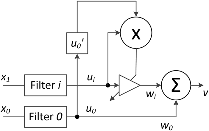
Illustration of the ICO learning model. The raw stimulus input x1 can trigger many different activation signals ui, which depend on the filters’ properties. The signal x0 acts as a reference that changes the synaptic weights wi in an unsupervised manner.
FIGURE 2
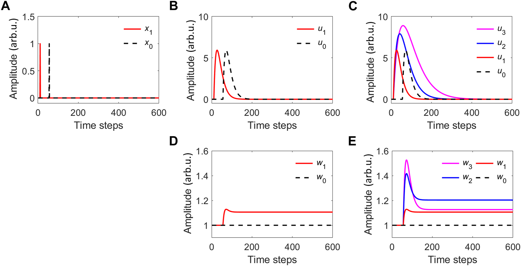
(A) Two delta-function raw inputs x1 and x0 with a time difference of T = 45 steps. (B) Their corresponding filtered activation signals (u1 and u0). (C) The corresponding filtered activation signals when considering three different filters for the stimulus signal x1. The filter parameters are: Q = 0.51 and c =1/(1+0.5 (i −1)), f =0.01/i for the three activation inputs u1, u2 and u3, and c =1, f =0.01 for u0. (D) The weights for the filtered activation signal of case (B). (E) The weights for the filtered activation signal of case (C).
When using only one filter for each raw input, x0 and x1, these are transformed by the filtering process into the activation signals u0 and u1 respectively (Figure 2B). We use the same filter for both signals, with Q = 0.51, c = 1, and f = 0.01. Then we apply the ICO rule in Eq. 1 to update the weight associated with the stimulus signal u1 (Figure 2D). Weight values change only during the time overlap between the increasing and decreasing parts of the filtered activation signals. The increasing part of the reference signal, captured by the first-order derivative, marks also the increasing part of the weight. In general, when the reference signal comes later than the stimulus signal, the weight increases. For example in Figure 2D, the weight goes from an initial value of 1 to eventually a value around 1.1. There is a short region of decrease, around the time steps 70–90, and this is due to the overlap between the final part of the stimulus signal and the decreasing part of the reference signal. The weight w1 then remains constant in the absence of overlap between u0 and u1.
The ICO learning rule can include multiple filtered versions of the original stimulus signal x1 to increase its range of operation and improve its input resolution. Each new filter is usually designed to expand in time the stimulus signal in a different manner. For instance, a reference signal x0 appearing at the 200th time step would not interact with activation filtered function u1 in Figure 2B. We numerically study the case with a bank of 3 filters that are applied to the raw input x1 (u1, u2, u3) (see Figure 2C). The filter bank increases the temporal range of ICO learning rule operation. Reference inputs appearing up to the 400th time step now interact with at least one filtered version of the stimulus signal. The filter parameters for the stimuli signal are Q = 0.51, c = 1/(1 + 0.5 (i − 1)), and fi = 0.1/i, where i > 0 is the increment number of the filter bank. In this particular case, the weights (w1, w2, w3) associated with the output of each filter (u1, u2, u3) follow the same trend as in the case of a single filter for the raw stimulus signal (Figure 2E). The filter bank adds expressive power to the ICO rule in resemblance with the way dendritic plasticity adds computational power to a single neuron. Dendrites do not just receive the input information (stimuli) and act as passive receivers; each dendritic branch can apply a different filter to the stimulus signal and then adapt the strength of the contribution of the dendritic branch (for a review see [45]).
2.2 Optoelectronic implementation of the ICO learning rule
In this work, we consider an optoelectronic dendritic unit (ODU) to implement the ICO learning rule. The ODU is an optoelectronic system with individual single-mode fiber optical paths (dendritic branches—DB) that can carry different information. In the context of the ICO learning topology, one DB is assigned to the transmission of the reference information, while the rest of the branches are assigned to the information from the sensory stimuli.
2.2.1 Experimental setup of an optoelectronic dendritic unit
The experimental design of a single-mode fiber (SMF) optoelectronic dendritic unit (ODU) with four dendritic branches, in a coincidence detection architecture, is shown in Figure 3. A 40 mW superluminescent diode (SLD) at 1,550 nm, followed by an optical isolator and a tunable-bandwidth optical filter, provides an incoherent optical carrier to the input of the ODU. The bandwidth of the filter is set to 1.5 nm so that the fiber lengths of the ODU do not introduce considerable chromatic dispersion that distorts the initial pulse shapes. The input information is encoded via a 10 GHz Mach-Zehnder modulator (MZM) biased at its quadrature operating point, using a time-multiplexing approach. Four independent data streams that correspond to the individual filtered stimuli (u3, u2, u1) and reference signals (u0) are combined into a single data stream in sequential order, with some time separation between them. Time-multiplexing allows the data stream to be electrically generated by a single channel (CH1) of a 9.6 GHz 24 GSa/s arbitrary waveform generator (AWG) and applied in the optical domain using only one MZM element. After encoding, the optical signal is split into four optical paths, via a 1 × 4 optical splitter, representing the four optical dendritic branches. Each path includes a semiconductor optical amplifier (SOA), which can amplify or attenuate the strength gi of the optical signal. The three DBs (#2, #3, and #4) that carry the experimental stimuli signals, need to be dynamically weighted, following the plasticity rules that apply at any given time. Thus, in these three dendritic branches, the SOAs are operated as modulators (SOAMOD) by using the appropriate circuitry and by modulating their bias current. The supporting modulation rates range from 1.5 MHz up to 2 GHz. The plasticity rules are introduced by the weight data streams (w3, w2, and w1), which are again combined into a single data stream in sequential order via time-multiplexing. Using a second AWG channel (CH2) and after electrical splitting (RFS), these weighted sequences are electrically amplified (RFA) and applied to the SOAMOD devices. In addition, each dendritic branch of the ODU incorporates an SMF spool (SMF-S) of increasing length (1, 1.5, 2, and 2.5 km), so that the time-multiplexed signals encoded at the input are temporally aligned at the coupling stage (4 × 1 optical coupler). By construction, the summation of the optical signals from the different paths is incoherent. An optical filter reduces the amplified spontaneous emission noise–introduced by both the SOA and SOAMOD devices—of the summed optical signal. Finally, the optical signal power is detected by an optical power meter (PM) and its temporal evolution is detected by a 20 GHz AC-coupled photoreceiver with a trans-impedance amplifier (PD). The converted electrical signal is monitored and recorded by a real-time 16 GHz analog bandwidth 40 GSa/s oscilloscope (OSC). The type and operating conditions of the components and instruments are provided in Table 1.
FIGURE 3
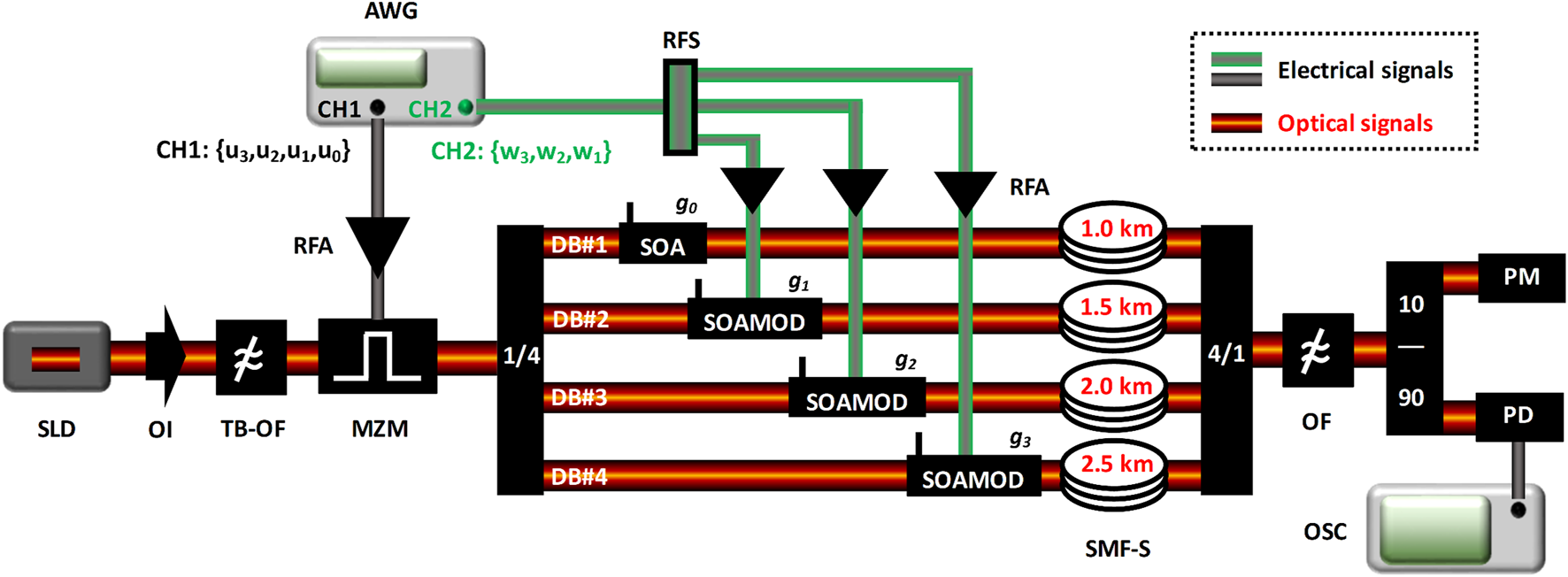
Optoelectronic dendritic unit (ODU) with four dendritic branches (DB), in a coincidence detection architecture. SLD, Superluminescent diode, OI, Optical isolator, TB-OF, Tunable-bandwidth optical filter, MZM, Mach-Zehnder modulator, 1/4, One-to-four optical splitter, SOA, Semiconductor optical amplifier, SOAMOD, Semiconductor optical amplifier operating as modulator, SMF-S, Single-mode fiber spool, 4/1, Four-to-one optical coupler, OF, Tunable optical filter, 10/90, Optical splitter, PM, Powermeter, PD, Photodetector, OSC, Real-time oscilloscope, AWG, Arbitrary waveform generator, RFA, RF amplifier, RFS, RF splitter.
TABLE 1
| Component | Provider | Model | Operating parameters |
|---|---|---|---|
| SLD | Thorlabs | SLD1550-A40 | I = 500 mA, T = 20 °C |
| TB-OF | Santec | OTF-350 | λ = 1,550 nm, Δλ = 1.5 nm |
| MZM | EOSpace | AZ-1K1-12 | Quadrature point |
| SOA | Thorlabs | SOA1117S | I = 170–230 mA, T = 20 °C |
| SOAMOD circuitry | Nanotech | BTY-T1SOA-XHS | - |
| SMF-S | j-fiber | SSMF-G652D-Ultra | - |
| PM | Thorlabs | PM100D | - |
| OF | Agiltron | FOTF-025121333 | λ = 1,550 nm |
| PD | Miteq | SCMR-100K20G | - |
| OSC | Lecroy | WaveMaster 816Zi-B | S = 10 GSa/s |
| AWG | Tektronix | AWG7122B | S = 10 GSa/s |
| RFA | iXblue | DR-VE-10-MO | Analog operation |
| RFS | RF-Lambda | RFLT2WDC27GA | - |
Components, instrumentation and operational parameters used in the ODU experiment. I: Bias current, T: Temperature, λ: Wavelength, Δλ: Wavelength bandwidth, S: Sampling rate.
2.2.2 Time-multiplexing for data encoding
By applying time-multiplexing, we significantly reduce the components that are needed to introduce independent sequences into the different optical dendritic branches. The time-multiplexing of the encoded data, the weighting, and the temporal compensation of the different dendritic branches work as follows. In CH1 of the AWG, we encode sequentially the following input data sets: u3, u2, u1, and finally u0 (Figure 4). Only when the temporal distance between these sequences matches the physical temporal delay introduced by the length of the ODU’s different DBs, the coincidence of the data sets will happen in predetermined dendritic branches. Specifically, the u3 sequence, which is encoded first, is assigned in DB #4 which has the longest delay (SMF-S of 2.5 km). u2 that is encoded second is assigned in DB #3 with the second longest delay (SMF-S of 2 km). u1 that is encoded third is assigned in DB #2 with the third longest delay (SMF-S of 1.5 km). Finally, u0 is encoded last and is assigned in DB #1 with the shortest delay (SMF-S of 1 km). As the physical propagation length of the DBs is fixed, the temporal matching is performed at the AWG encoding by setting the appropriate temporal spacing ΔTuij between the input data sets. The temporal resolution we use for this matching is 100 ps and is defined by the AWG. The length difference of ∼ 500 m between adjacent DBs introduces delays among the optical signals of ∼ 2.45 μs. This delay defines the maximum length of the data sets ui that can be encoded with time-multiplexing, without overlapping with each other. Eventually, at the summation point - the 4 × 1 optical coupler’s output - the experimental signals that correspond to the four encoded data sets (ui, i = 0–3) are temporally aligned. In absence of weighting adaptation and for various optical strengths gi of the DBs, the corresponding optical signals are summed in the photodetected ODU output vE:In Eq. 4, we consider that the encoded signals ui undergo a linear transformation through the physical ODU system, thus their measured values are approximated by a simple multiplication with a gain value. When introducing adaptive weighting in three out of the four dendritic branches, another temporal alignment is required. The time-multiplexed sequences that carry the weight information are uploaded at the encoding stage, in CH2 of the AWG. The weight data sets (w3, w2, and w1) are encoded sequentially. Here, the physical path of the electrical lines and the optical paths are again fixed. Thus, temporal matching is performed via the AWG encoding, by setting the appropriate temporal spacing ΔTwij between the weight data sets, but also the appropriate temporal shift ΔTuw with respect to the input signal sequence u (Figure 4). In this way, there is a pre-defined time window in which the optical signals that carry the weighted data sets are temporally aligned and summed at the summation stage (the 4 × 1 optical coupler’s output, Figure 4, red dashed box). Also, in this case, the experimentally applied weights to the optoelectronic system are approximated by a linear transformation of the encoded weight data sets (wi). The photodetected ODU output vE with weighting adaptation is given by:
FIGURE 4
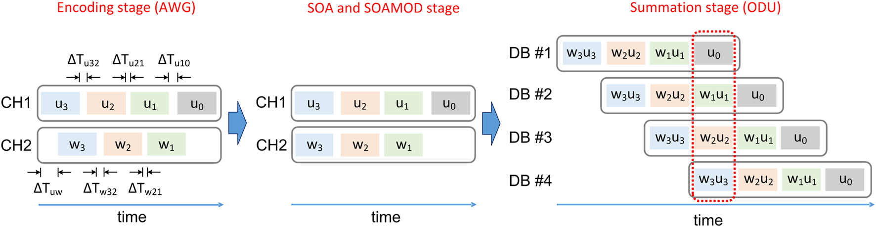
Schematic diagram of the time-multiplexing encoding and the coincidence detection at the ODU output. The temporal distances between the encoded input ui (CH1) and weight wi (CH2) data sets are defined so that there is a predefined time window for the ODU summation stage in which the different, individual signals that propagate along the dendritic branches DB are temporally aligned and summed.
3 Results
3.1 Performance of the ICO learning rule—Numerical results
We show in Figure 5 two cases with different parameter sets for the numerical implementation of the ICO rule. These results illustrate the impact of the time difference between the activation signals of the stimulus (u1) and the reference (u0) to the change of the weight w1 associated to the stimulus branch, and the corresponding output v. In Figure 5A, four pulses are repeated every 600 time steps, under the condition that u1 comes T = 55 time steps before u0. For the next three pulses, u0 is zero, while the last 4 pulses of u1 come after u0 with a time difference of T = −55 steps. For this case, a learning rate of η = 0.05 in Eq. 1 is considered. In the case of Figure 5B, the four pulses are repeated every 600 time steps, under the condition that u1 comes now at T = 20 time steps before u0. For the next three pulses, u0 is zero, while the last four u1 pulses come after u0 with a shorter time difference of T = −20 time steps. For this case, a slower learning rate η = 0.01 in Eq. 1 is considered. In both cases, the initial plastic weight (w1) increases when the interval T between the two inputs is positive and decreases when it is negative; the weight remains constant if one of the inputs is zero (Figures 5A, B, middle graphs). The weight increase is linear and depends on the learning rate (η) and the time interval between inputs (T). The output of the ICO learning rule v is given in (Figures 5A, B, lower graphs), for the two cases.
FIGURE 5
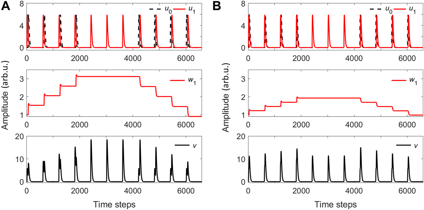
(A) Top panel: A sequence of two activation inputs u0 and u1, with u0 obeying different conditions: it appears after u1 with T =55 time steps, it is zero, or it appears before u1 with T =−55 time steps. Middle panel: The plastic weight w1. Bottom panel: The ICO learning output v. The learning rate is η =0.05 and w0=1. (B) Same as A, but with a reduced temporal separation between u1 and u0 (T =20 or T =−20 time steps) and smaller learning rate η =0.01.
The values of the stimulus activation inputs play a decisive role in the calculation of their weights. Until now, we have considered input sequences in which the pulse amplitude returns to zero. However, if the input sequences have a DC bias (b), the ICO learning rule implies different weight updates according to Eq. 1. A stimulus input signal with bias (u1 + b) leads to a different weight update, with respect to an input signal without bias. In contrast, a bias value in the reference input only affects the output signal but not the weight update. This is shown in Figure 6, by considering two cases with minimum amplitude (or DC bias) of b = 2.5 and b = 5. When comparing the above behavior with the case of b = 0 (dashed red line in Figure 6), we conclude that the bias increases the average value of the ICO learning output v and the plastic weight w1, but the behavior regarding the time difference steps between the inputs remains the same. The reason for which we consider this DC bias is to take into account the characteristics of our experimental demonstration. On the one hand, the light source that we use in our experiment (SLD) is non-monochromatic, with an optical bandwidth set to 1.5 nm, leading to incoherent positive summations only. On the other hand, external optical modulation is performed via an optical MZM, an interferometric device that is designed for coherent light. Thus, when a given wavelength condition matches the maximum extinction ratio obtained at the optical output of the MZM, the neighboring wavelengths do not comply with this interferometric condition. Thus, there will always be significant optical power at the lowest modulation level of our optical input signal, i.e. a DC bias in the optical input.
FIGURE 6
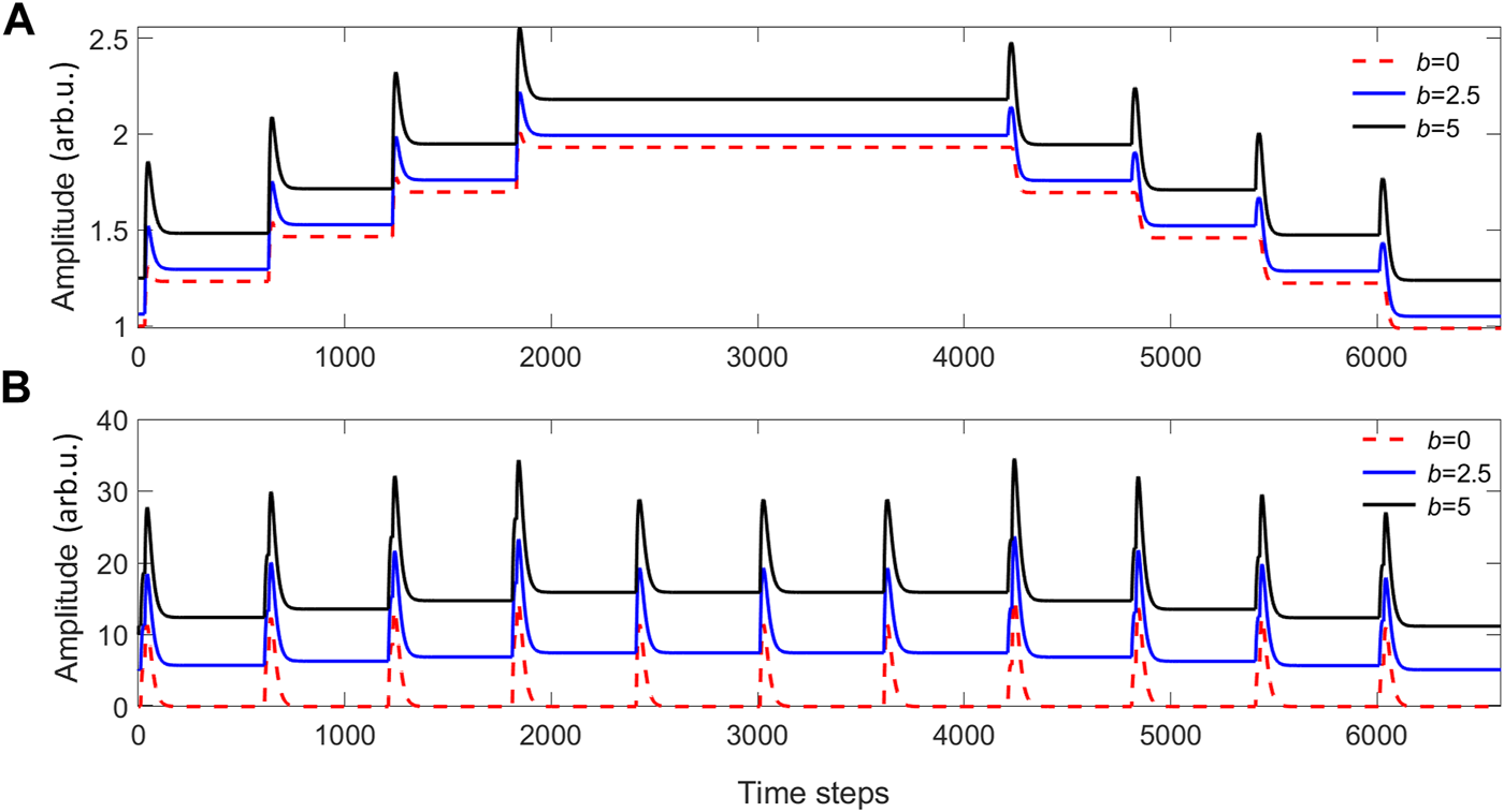
(A) The plastic weights w1, and (B) the ICO learning outputs v, for different DC amplitude bias values b of the activation inputs presented in Figure 5B. The learning rate is η =0.01 and w0=1.
Next, we numerically study the case with a bank of 3 filters that are applied to the raw input x1 leading to three different activation signals u1, u2 and u3, following the general ICO learning concept of Figure 1. Here, we consider a total of twenty input time frames, in which raw stimuli and reference pulses are repeated every 600 time steps, with different time distances between them. In the first eight input time frames, x0 is delayed by T = 45 time steps with respect to x1; in the next four time frames the reference signal x0 is zero; in the last eight frames, x0 is 45 time steps ahead of x1 (T = −45). The filtered raw inputs result in the activation input sequences ui of Figure 7A. These filtered inputs are applied to the ICO learning rule with a learning rate of η = 0.01 and a weight for the reference signal equal to w0 = 1. The ICO learning output v signal is shown in Figure 7B, while the update of the adaptive weights wi (i > 0) is shown in Figure 7C. The differences among the plastic weights wi are given by the different input activation amplitudes ui and the time overlap between the stimuli filtered signals and the reference one.
FIGURE 7
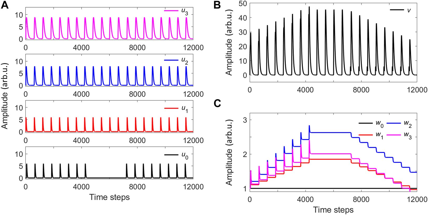
Numerical simulations of the ICO rule with one stimulus signal x1 that feeds three different activation filters (u1− u3). (A) Input activation signals (reference and stimuli). (B) Output of the ICO rule. (C) Plastic weights that correspond to the stimuli activation inputs.
3.2 Performance of the ICO learning rule—Experimental results
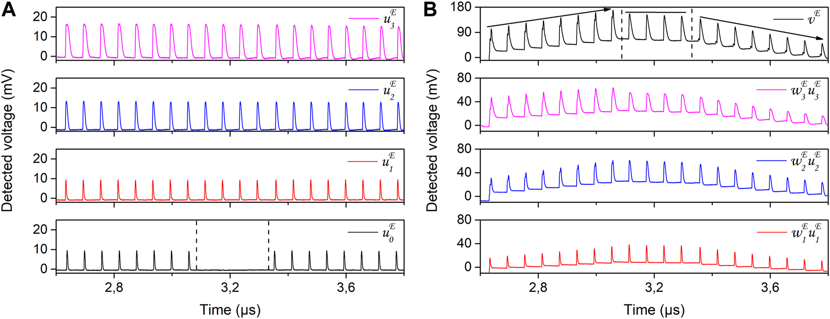
The filtered inputs (u0, u1, u2, u3) and weights (w1, w2, w3, are applied in the experimental realization of the ODU, using the time-multiplexing approach explained in Section 2.2.2. We apply the two corresponding sequences u and w to the two channels of the AWG (Figure 3). Appropriate scaling of the electrical modulating sequences is applied. This scaling defines the modulation depth of the optical carriers for each dendritic branch. However, as discussed in the previous section, the incoherent nature of the incoming optical signal sets a non-zero optical signal for the lowest modulation values, introducing a DC bias to the overall experimentally recorded sequence. The SOA and SOAMOD bias currents are tuned to equalize the average optical power of each dendritic branch. As the different DBs experience slightly different optical losses, the provided gain gi in each path may be slightly different for this optical power equalization. In Figure 8A, we show the experimentally measured filtered input signals , as they are detected at the output of the ODU, in the absence of the rest of the inputs and plastic weight application. The detected amplitudes of the signals become consistent with the numerically computed ones (Figure 7A) by adjusting the gain gi of each DB, which is incorporated in the amplitude . The DC bias of each input is not depicted here, as the optoelectronic detection of the ODU is performed with an AC-coupled photoreceiver. In Figure 9, we show a zoom of the measured signals for the four DBs, and for the three different u0 conditions studied in the corresponding encoded sequence. Specifically, in Figure 9A, the measured signal (black line) fires after the stimuli filtered input signals (, i = 1–3); in Figure 9B, is zero; and in Figure 9C, fires before the stimuli inputs.
FIGURE 8
ICO rule applied to the experimental ODU in an open loop configuration. (A) Measured filtered input signals that propagate along the four DBs before weighting, in absence of weighting and the rest of the inputs. The dashed lines separate the three different reference filtered input signal conditions. (B) Weighted filtered input signals in the three plastic DBs and ODU output signal (vE). The weights are obtained from the SOAMODs electro-optic response, after feeding the numerically calculated values wi. The experimentally measured signals are obtained at the ODU output.
FIGURE 9
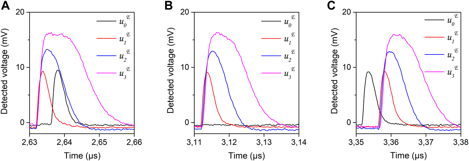
Detail of Figure 8, focusing on the three different timing conditions of the reference filtered signal (black line). In (A) fires after the stimuli filtered inputs ; in (B) is zero; in (C) fires before the stimuli filtered inputs . All filtered input signals are monitored experimentally by their physical counterpart .
In the next step, we apply the pre-calculated weights in the dendritic branches that carry the stimuli information (DB#2-DB#4). In Figure 8B we show the individually measured signals after weighting , as they are detected at the output of the ODU, in absence of the rest of the inputs. We also show the output summation detected signal vE, in which three distinct regimes can be identified, in agreement with the numerically computed output of the ICO learning rule of Figure 7. The first eight pulses include a reference signal that rises in time after the stimuli signals (, , and ), as seen in Figure 9A. The experimental ODU output results in an increase of the peak amplitude for these first eight pulses (Figure 8B), every time a reference pulse appears and is lagging the stimuli pulses. The first peak has an amplitude of 103 mV, while the 8th peak’s amplitude is increased to 169 mV. The next four stimuli pulses are not accompanied by any reference pulse (Figure 9B) and, consequently, the output pulses preserve the same amplitude, with only a very slight decrease. The amplitude values vary within the range of 148 mV–156 mV. Finally, the last eight stimuli pulses of , , and are accompanied by a leading reference signal (Figure 9C). In the latter case, the ICO learning rule results in a decrease of the peak amplitude at the ODU output, every time a reference pulse appears. The last peak of the sequence is obtained with an amplitude of 50 mV.
The deviation that we find between the numerically computed ICO learning output v (Figure 7) and the corresponding experimental one vE (Figure 8) is mainly due to the DC bias of the experimental input signals. As we showed in Figure 6, if the pulses do not return to zero, the ODU output will also not return to zero between pulses. This is the case of the experimental implementation, as a “zero” value encoding at the input, results always in non-zero optical power for the optical signals that propagate through the dendritic branches. This DC bias results in the non-return-to-zero pulse behavior in Figure 8B. This effect was not considered in the numerical computation of Figure 7, which were obtained assuming a DC bias b = 0 and no gain (i.e. g = gi = 1). There, the ODU output exhibits return-to-zero pulses (Figure 7B). In an updated numerical implementation of the ICO learning rule, we consider now a DC bias b = 8 and a gain of g = gi = 2 for i = 0–3, with these values emulating best the corresponding experimental parameters. By recalculating the ICO learning rule we obtain the output in Figure 10. Now the numerically computed output (Figure 10A, black line) shows a non-return-to-zero pulse behavior, in accordance with the experimentally computed sequence (Figure 10A, red line). The individually weighted signals, for each dendritic branch of the stimuli, show also a non-return-to-zero pulse behavior (Figure 10B) and are also in agreement with the corresponding experimental signals of Figure 8B.
FIGURE 10
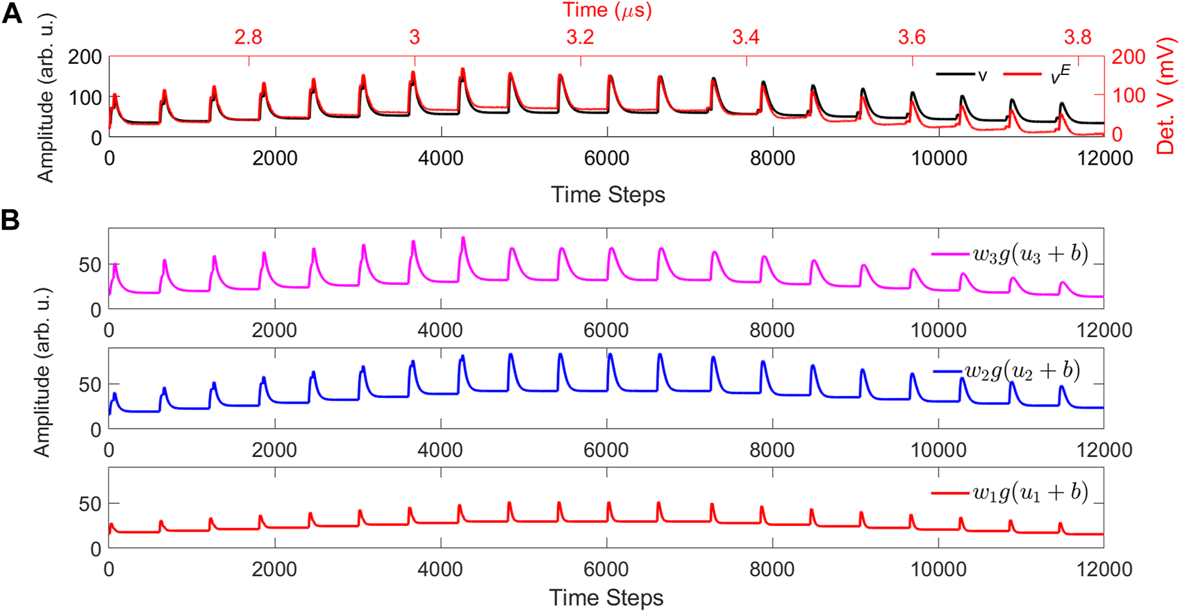
(A) Comparison between numerical simulations (v, black color) and experimental results (vE, red color) of the ICO rule’s output, with one stimulus signal x1 that feeds three activation filters (u1− u3). In the numerical model, the gain is g =2 and the bias is b =8. “Det. V” is the abbreviation for “Detected Voltage.” (B) The numerically computed weighted stimulus input signals, for the previous values of gain g and bias.
We can see in Figure 10A that, after adjusting and including both parameters of gain and bias in the numerical computation, we obtain an overall good agreement between the numerical output and the experimentally obtained results at the ODU output. There is only a small divergence between the two signals in the last part of the sequence, due to the faster decay of the experimentally detected output compared to the numerically calculated one. The reason is that the SOAMOD circuitry introduces a non-negligible attenuation in the low-frequency modulation, leading to a stronger decay of the DC-detected signal than numerically expected. This is because the total duration of the signal we process is 1.2 μs (as shown in Figure 10A), which corresponds to a frequency of 833 kHz, slightly below the low cut-off frequency of the SOAMOD circuitry (1.5 MHz).
4 Discussion
The presented optoelectronic ODU and the proof-of-concept implementation of the ICO learning rule, in an open loop configuration and at the nanosecond scale, open the path for future control and adaptation in ultra-fast optoelectronic hardware platforms. Further advances of the presented system can already be envisaged, toward more compact and energy-efficient designs, by transferring the proposed ODU design to photonic integrated platforms, where the fiber-based dendritic branches are substituted by optical waveguides. Here, we made use of incoherent optical signals, which hampers signal subtraction. In a photonic integrated circuit platform, a fully-controllable phase-dependent ODU approach could be considered, while replacing the power-expensive SLD with a coherent laser source. Then, the subtraction of coherent signals would be possible via the appropriate optical phase-sensitive control of the dendritic branches, by exploiting the properties of phase-change materials [46–48]), or graphene ([49]) for phase modulation. A coherent approach would also eliminate the optical bias that appears now in the fiber-based ODU, at the input signal modulation stage. This would allow also an easier parametrization of the system and convergence between the experimental results and the numerically calculated ICO learning performance. Additionally, in the presented ODU, the incorporation of SOAMOD devices offers the flexibility to amplify individually the optical signals in the dendritic branches, apart from the application of the weights. In a photonic integrated platform, the weight adaptation could be introduced by integrated lithium-niobate [50, 51] or microring resonator [52, 53] modulators, in absence of any optical amplification means. Eventually, the optical power budget of the ODU will determine the number of dendritic branches that could be considered without amplification, in energy-efficient designs.
The optoelectronic ODU could also be exploited in a closed-loop configuration for control applications. ICO learning was originally proposed as a model that describes how an agent can learn an anticipatory action to react and avoid a reflex event that is preceded by an earlier alarm signal. As shown by one of the authors [41, 54], the ICO learning rule in a closed-loop approach can be used in various control applications, where the reaction to a sensory stimulus x1 can be adapted by the ICO learning to predict and eventually suppress the occurrence of a reflex behavior. In such closed-loop feedback control applications, the reference input is an error signal for the learning while the stimulus or sensory inputs xi>0 will be an early alarm signal. Extending the presented ODU implementation to operate in a closed loop means that the adaptation weights - which in this study were pre-computed and uploaded in the experimental setup - would need to be calculated in real-time from the output signal, for each temporal resolution step and applied to the ODU. Although this approach would still require some conventional computational processing, it would demonstrate an autonomous operation of an ODU that implements the ICO learning rule. Finally, this ODU implementation will serve as a flexible photonic testbed for other synaptic plasticity rules beyond the ICO learning and the exploration of more advanced forms of dendritic computing. This concept could be transferred for dedicated computing tasks into more compact, energy-efficient photonic integrated circuits or memristive platforms.
Statements
Data availability statement
The raw data supporting the conclusion of this article will be made available by the authors, without undue reservation.
Author contributions
SO performed the numerical simulations of the study, in collaboration with CT, FW, and AA. AA designed and implemented the experimental ODU, conducted the experiment and analyzed the corresponding data. SO, MS, CM, and AA drafted the paper. All authors participated in the conceptual design of this study, the discussion of the results, and the final writing of the paper.
Funding
The authors acknowledge the support of the European Union’s Horizon 2020 research and innovation programme under grant agreement No. 899265 (ADOPD), and the fruitful discussions with Robert Legenstein and the rest scientific collaborators that participate in this project.
Conflict of interest
The authors declare that the research was conducted in the absence of any commercial or financial relationships that could be construed as a potential conflict of interest.
The handling editor LP declared a past co-authorship with the authors CRM, AA.
Publisher’s note
All claims expressed in this article are solely those of the authors and do not necessarily represent those of their affiliated organizations, or those of the publisher, the editors and the reviewers. Any product that may be evaluated in this article, or claim that may be made by its manufacturer, is not guaranteed or endorsed by the publisher.
References
1.
Abbott LF Nelson SB . Synaptic plasticity: Taming the beast. Nat Neurosci (2000) 3:1178–83. 10.1038/81453
2.
Saïghi S Mayr CG Serrano-Gotarredona T Schmidt H Lecerf G Tomas J et al Plasticity in memristive devices for spiking neural networks. Front Neurosci (2015) 9:51. 10.3389/fnins.2015.00051
3.
Acharya J Basu A Legenstein R Limbacher T Poirazi P Wu X . Dendritic computing: Branching deeper into machine learning. Neuroscience (2022) 489:275–89. 10.1016/j.neuroscience.2021.10.001
4.
Beniaguev D Segev I London M . Single cortical neurons as deep artificial neural networks. Neuron (2021) 109:2727–39.e3. 10.1016/j.neuron.2021.07.002
5.
London M Häusser M . Dendritic computation. Annu Rev Neurosci (2005) 28:503–32. 10.1146/annurev.neuro.28.061604.135703
6.
Indiveri G Linares-Barranco B Hamilton TJ Schaik AV Etienne-Cummings R Delbruck T et al Neuromorphic silicon neuron circuits. Front Neurosci (2011) 5:73. 10.3389/fnins.2011.00073
7.
Chicca E Stefanini F Bartolozzi C Indiveri G . Neuromorphic electronic circuits for building autonomous cognitive systems. Proc IEEE (2014) 102:1367–88. 10.1109/jproc.2014.2313954
8.
Marković D Mizrahi A Querlioz D Grollier J . Physics for neuromorphic computing. Nat Rev Phys (2020) 2:499–510. 10.1038/s42254-020-0208-2
9.
Serrano-Gotarredona T Masquelier T Prodromakis T Indiveri G Linares-Barranco B . STDP and STDP variations with memristors for spiking neuromorphic learning systems. Front Neurosci (2013) 7:2. 10.3389/fnins.2013.00002
10.
Burr GW Shelby RM Sebastian A Kim S Kim S Sidler S et al Neuromorphic computing using non-volatile memory. Adv Phys X (2017) 2:89–124. 10.1080/23746149.2016.1259585
11.
Boybat I Le Gallo M Nandakumar S Moraitis T Parnell T Tuma T et al Neuromorphic computing with multi-memristive synapses. Nat Commun (2018) 9:2514. 10.1038/s41467-018-04933-y
12.
Upadhyay NK Jiang H Wang Z Asapu S Xia Q Joshua Yang J . Emerging memory devices for neuromorphic computing. Adv Mater Tech (2019) 4:1800589. 10.1002/admt.201800589
13.
Sangwan VK Hersam MC . Neuromorphic nanoelectronic materials. Nat Nanotechnology (2020) 15:517–28. 10.1038/s41565-020-0647-z
14.
Wang R Yang JQ Mao JY Wang ZP Wu S Zhou M et al Recent advances of volatile memristors: Devices, mechanisms, and applications. Adv Intell Syst (2020) 2:2000055. 10.1002/aisy.202000055
15.
Torrejon J Riou M Araujo FA Tsunegi S Khalsa G Querlioz D et al Neuromorphic computing with nanoscale spintronic oscillators. Nature (2017) 547:428–31. 10.1038/nature23011
16.
Grollier J Querlioz D Camsari K Everschor-Sitte K Fukami S Stiles MD . Neuromorphic spintronics. Nat Electron (2020) 3:360–70. 10.1038/s41928-019-0360-9
17.
van De Burgt Y Melianas A Keene ST Malliaras G Salleo A . Organic electronics for neuromorphic computing. Nat Electron (2018) 1:386–97. 10.1038/s41928-018-0103-3
18.
Shastri BJ Tait AN Ferreira de Lima T Pernice WH Bhaskaran H Wright CD et al Photonics for artificial intelligence and neuromorphic computing. Nat Photon (2021) 15:102–14. 10.1038/s41566-020-00754-y
19.
Dabos G Bellas DV Stabile R Moralis-Pegios M Giamougiannis G Tsakyridis A et al Neuromorphic photonic technologies and architectures: Scaling opportunities and performance frontiers [invited]. Opt Mater Express (2022) 12:2343–67. 10.1364/ome.452138
20.
Larger L Soriano MC Brunner D Appeltant L Gutierrez JM Pesquera L et al Photonic information processing beyond turing: An optoelectronic implementation of reservoir computing. Opt express (2012) 20:3241–9. 10.1364/oe.20.003241
21.
Brunner D Soriano MC Mirasso CR Fischer I . Parallel photonic information processing at gigabyte per second data rates using transient states. Nat Commun (2013) 4:1364. 10.1038/ncomms2368
22.
Romeira B Avó R Figueiredo JM Barland S Javaloyes J . Regenerative memory in time-delayed neuromorphic photonic resonators. Scientific Rep (2016) 6:19510. 10.1038/srep19510
23.
Deng T Robertson J Wu ZM Xia GQ Lin XD Tang X et al Stable propagation of inhibited spiking dynamics in vertical-cavity surface-emitting lasers for neuromorphic photonic networks. IEEE Access (2018) 6:67951–8. 10.1109/access.2018.2878940
24.
Borghi M Biasi S Pavesi L . Reservoir computing based on a silicon microring and time multiplexing for binary and analog operations. Scientific Rep (2021) 11:15642. 10.1038/s41598-021-94952-5
25.
Bueno J Maktoobi S Froehly L Fischer I Jacquot M Larger L et al Reinforcement learning in a large-scale photonic recurrent neural network. Optica (2018) 5:756–60. 10.1364/optica.5.000756
26.
Heuser T Pfluger M Fischer I Lott JA Brunner D Reitzenstein S . Developing a photonic hardware platform for brain-inspired computing based on 5× 5 vcsel arrays. J Phys Photon (2020) 2:044002. 10.1088/2515-7647/aba671
27.
Tait AN De Lima TF Zhou E Wu AX Nahmias MA Shastri BJ et al Neuromorphic photonic networks using silicon photonic weight banks. Scientific Rep (2017) 7:7430. 10.1038/s41598-017-07754-z
28.
Peng HT Nahmias MA De Lima TF Tait AN Shastri BJ . Neuromorphic photonic integrated circuits. IEEE J Selected Top Quan Electron (2018) 24:1–15. 10.1109/jstqe.2018.2840448
29.
Van der Sande G Brunner D Soriano MC . Advances in photonic reservoir computing. Nanophotonics (2017) 6:561–76. 10.1515/nanoph-2016-0132
30.
Toole R Tait AN De Lima TF Nahmias MA Shastri BJ Prucnal PR et al Photonic implementation of spike-timing-dependent plasticity and learning algorithms of biological neural systems. J Lightwave Technol (2015) 34:470–6. 10.1109/jlt.2015.2475275
31.
Alanis JA Robertson J Hejda M Hurtado A . Weight adjustable photonic synapse by nonlinear gain in a vertical cavity semiconductor optical amplifier. Appl Phys Lett (2021) 119:201104. 10.1063/5.0064374
32.
De Lima TF Peng HT Tait AN Nahmias MA Miller HB Shastri BJ et al Machine learning with neuromorphic photonics. J Lightwave Technol (2019) 37:1515–34. 10.1109/jlt.2019.2903474
33.
Xu X Tan M Corcoran B Wu J Boes A Nguyen TG et al 11 TOPS photonic convolutional accelerator for optical neural networks. Nature (2021) 589:44–51. 10.1038/s41586-020-03063-0
34.
Huang C Sorger VJ Miscuglio M Al-Qadasi M Mukherjee A Lampe L et al Prospects and applications of photonic neural networks. Adv Phys X (2022) 7:1981155. 10.1080/23746149.2021.1981155
35.
Zhou H Dong J Cheng J Dong W Huang C Shen Y et al Photonic matrix multiplication lights up photonic accelerator and beyond. Light: Sci Appl (2022) 11:30. 10.1038/s41377-022-00717-8
36.
El Srouji L Krishnan A Ravichandran R Lee Y On M Xiao X et al Photonic and optoelectronic neuromorphic computing. APL Photon (2022) 7:051101. 10.1063/5.0072090
37.
Löwel S Singer W . Selection of intrinsic horizontal connections in the visual cortex by correlated neuronal activity. Science (1992) 255:209–12. 10.1126/science.1372754
38.
Tong R Chater TE Emptage NJ Goda Y . Heterosynaptic cross-talk of pre- and postsynaptic strengths along segments of dendrites. Cel Rep (2021) 34:108693. 10.1016/j.celrep.2021.108693
39.
Royer S Paré D . Conservation of total synaptic weight through balanced synaptic depression and potentiation. Nature (2003) 422:518–22. 10.1038/nature01530
40.
Bailey CH Giustetto M Huang YY Hawkins RD Kandel ER . Is heterosynaptic modulation essential for stabilizing hebbian plasiticity and memory. Nat Rev Neurosci (2000) 1:11–20. 10.1038/35036191
41.
Porr B Wörgötter F . Strongly improved stability and faster convergence of temporal sequence learning by using input correlations only. Neural Comput (2006) 18:1380–412. 10.1162/neco.2006.18.6.1380
42.
Porr B Wörgötter F . Isotropic sequence order learning. Neural Comput (2003) 15:831–64. 10.1162/08997660360581921
43.
Goldschmidt D Wörgötter F Manoonpong P . Biologically-inspired adaptive obstacle negotiation behavior of hexapod robots. Front Neurorobotics (2014) 8:3. 10.3389/fnbot.2014.00003
44.
Möller K Kappel D Tamosiunaite M Tetzlaff C Porr B Wörgötter F . Differential hebbian learning with time-continuous signals for active noise reduction. Plos one (2022) 17:e0266679. 10.1371/journal.pone.0266679
45.
Payeur A Béïque JC Naud R . Classes of dendritic information processing. Curr Opin Neurobiol (2019) 58:78–85. 10.1016/j.conb.2019.07.006
46.
Cheng Z Ríos C Pernice WH Wright CD Bhaskaran H . On-chip photonic synapse. Sci Adv (2017) 3:e1700160. 10.1126/sciadv.1700160
47.
Feldmann J Youngblood N Wright CD Bhaskaran H Pernice WH . All-optical spiking neurosynaptic networks with self-learning capabilities. Nature (2019) 569:208–14. 10.1038/s41586-019-1157-8
48.
Brückerhoff-Plückelmann F Feldmann J Wright CD Bhaskaran H Pernice WH . Chalcogenide phase-change devices for neuromorphic photonic computing. J Appl Phys (2021) 129:151103. 10.1063/5.0042549
49.
Sorianello V Midrio M Contestabile G Asselberghs I Van Campenhout J Huyghebaert C et al Graphene–silicon phase modulators with gigahertz bandwidth. Nat Photon (2018) 12:40–4. 10.1038/s41566-017-0071-6
50.
Boes A Corcoran B Chang L Bowers J Mitchell A . Status and potential of lithium niobate on insulator (lnoi) for photonic integrated circuits. Laser Photon Rev (2018) 12:1700256. 10.1002/lpor.201700256
51.
Li M Ling J He Y Javid UA Xue S Lin Q . Lithium niobate photonic-crystal electro-optic modulator. Nat Commun (2020) 11:4123. 10.1038/s41467-020-17950-7
52.
Hu Y Xiao X Xu H Li X Xiong K Li Z et al High-speed silicon modulator based on cascaded microring resonators. Opt express (2012) 20:15079–85. 10.1364/oe.20.015079
53.
Li G Krishnamoorthy AV Shubin I Yao J Luo Y Thacker H et al Ring resonator modulators in silicon for interchip photonic links. IEEE J Selected Top Quan Electron (2013) 19:95–113. 10.1109/jstqe.2013.2278885
54.
Wörgötter F Porr B . Temporal sequence learning, prediction, and control: A review of different models and their relation to biological mechanisms. Neural Comput (2005) 17:245–319. 10.1162/0899766053011555
Summary
Keywords
optoelectronic system, input correlation learning, optical dendrites, optical computing, coincidence detection
Citation
Ortín S, Soriano MC, Tetzlaff C, Wörgötter F, Fischer I, Mirasso CR and Argyris A (2023) Implementation of input correlation learning with an optoelectronic dendritic unit. Front. Phys. 11:1112295. doi: 10.3389/fphy.2023.1112295
Received
30 November 2022
Accepted
01 March 2023
Published
15 March 2023
Volume
11 - 2023
Edited by
Lorenzo Pavesi, University of Trento, Italy
Reviewed by
Zi Wang, University of Delaware, United States
Gyorgy Csaba, Pázmány Péter Catholic University, Hungary
Updates
Copyright
© 2023 Ortín, Soriano, Tetzlaff, Wörgötter, Fischer, Mirasso and Argyris.
This is an open-access article distributed under the terms of the Creative Commons Attribution License (CC BY). The use, distribution or reproduction in other forums is permitted, provided the original author(s) and the copyright owner(s) are credited and that the original publication in this journal is cited, in accordance with accepted academic practice. No use, distribution or reproduction is permitted which does not comply with these terms.
*Correspondence: Apostolos Argyris, apostolos@ifisc.uib-csic.es
This article was submitted to Optics and Photonics, a section of the journal Frontiers in Physics
Disclaimer
All claims expressed in this article are solely those of the authors and do not necessarily represent those of their affiliated organizations, or those of the publisher, the editors and the reviewers. Any product that may be evaluated in this article or claim that may be made by its manufacturer is not guaranteed or endorsed by the publisher.