 Chang Chang
 Xiaoping Xie1,2*
- 1State Key Laboratory of Transient Optics and Photonics, Xi’an Institute of Optics and Precision Mechanics, Chinese Academy of Science, Xi’an, Shaanxi, China
- 2University of Chinese Academy of Science, Beijing, China
- 3School of Electronic Engineering, Xi’an University of Posts and Telecommunications, Xi’an, China
- 4School of Information Engineering, Sanming University, Sanming, China
The design of vertical and lateral PIN Ge-on-Si photodetectors was motivated by the disparity in electron and hole mobilities. In the case of vertical PIN junction detectors, configuring the slab region as n-type doping leads to a notable increase in the bandwidth of approximately 20 GHz compared to utilizing p-type doping for the slab. For lateral PIN junction detectors, we determined that setting the length of the n-type slab region to be 2.8 times that of the p-type slab region, based on the carrier saturation drift rate ratio, does not compromise the bandwidth. This configuration enhances the bandwidth while minimizing light absorption loss from the electrode. The proposed design in this study enhances the performance of Ge-on-Si photodetectors without adding complexity to the fabrication process. The principles applied in this study serve as instructive references for the conceptualization of other photonic or electronic devices, reinforcing the widespread applicability of these design strategies.
1 Introduction
Silicon photonics technology has attracted extensive research interest due to their CMOS process compatibility, low power consumption, and high integration [1–3]. A Ge-on-Si photodetector is one of the key components in a transceiver system, and its performance plays a decisive role in the transmission capacity [4–6]. Plenty of works have been carried out on Ge-on-Si photodetector’s design, and a series of progress has already been made in recent years [7–12]. However, its properties need further improvement for the application in 5G communication, optical computation, unmanned driving, and optical sensing [13–15]. Ge-on-Si photodetectors are currently available in two main structures: vertical and lateral PIN junctions. Vertical PIN junction photodetectors have been shown to achieve a larger bandwidth due to their more uniform electric field distribution, as demonstrated in previous studies [8–10]. On the other hand, lateral PIN junction devices exhibit a higher responsivity by minimizing light loss attributed to the absence of electrodes within their germanium absorption regions [6, 11, 12]. In the case of vertical PIN junction photodetectors, the top layer of germanium, being unintentionally doped and exhibiting n-type characteristics, is typically subjected to n-doping. Consequently, the bottom slab region of these detectors is p-doped [10]. As for lateral PIN junction detectors, reported designs, to the best of our knowledge, have utilized equal lengths for both the n-type and p-type slab regions [6, 11, 12].
Opto-electronic 3-dB bandwidth, responsivity, and dark current are critical performance indicators for Ge-on-Si photodetectors. Achieving a balance between bandwidth and responsivity is crucial due to their interdependency, and as a result, the design of photodetectors aims for optimization [16–18]. The distance between electrodes in Ge-on-Si photodetectors has a significant impact on both carrier transport time and parasitic capacitance. Decreasing the electrode distance reduces the carrier transport time but increases the parasitic capacitance, while increasing the electrode distance has the opposite effect. However, an important factor that has often been overlooked in the optimization process is the substantial difference in mobility between electrons and holes within silicon. This disparity in mobility between the two carrier types introduces additional complexities that should be taken into account to further improve the design and performance of Ge-on-Si photodetectors. By considering the disparate mobility characteristics of electrons and holes, it is possible to develop optimized designs that harness the full potential of these devices. In the n-type slab of Ge-on-Si photodetectors, the major carriers are electrons with a mobility of approximately 1,230 cm2/(Vs), while in the p-type slab, the major carriers are holes with a mobility of around 480 cm2/(Vs) [12]. By adjusting the lengths of the n-type and p-type slabs accordingly, it is possible to achieve an ideal match in the duration of electrons and holes within the PIN junction. This adjustment not only optimizes the parasitic capacitance between the electrodes but also enhances the overall performance of the photodetectors. By exploiting the disparity in carrier mobilities, we can further improve the performance of Ge-on-Si photodiodes without the need for additional fabrication processes. In this study, we focused on optimizing the structure of the Ge-on-Si photodiodes and conducted a thorough analysis of the characteristics exhibited by both vertical and lateral PIN junctions, taking into account the difference in carrier mobility.
2 Device design
Two distinct vertical PIN junction photodetector structures were designed and illustrated in Figure 1. The first device (Figure 1A) features a p-type germanium absorption region, an n-type silicon rib waveguide, and an n-type slab region. The second device (Figure 1B) employs an inverse doping configuration with an n-type germanium absorption region, a p-type doped silicon rib, and a p-type slab region. It merits mentioning that the n-type germanium absorption layer represents the typical architecture for vertical Ge-on-Si photodetectors. However, alternative structures such as p-type doped germanium are also available and have been documented in the prior literature studies [5, 19]. This underlines the flexibility and diversity inherent in the design of such optoelectronic devices. In our design, the silicon rib waveguide has a thickness of 220 nm and a width of 1.5 μm. The slab region, which is 60 nm thick, spans a width of 1.5 μm and is positioned between the edge of the core waveguide and the electrode. The germanium region has a thickness of 600 nm and a width of 1.5 μm [11]. The photodetector length, germanium layer, and electrode are all set to 10 μm for our calculations. The doping concentration in the p- and n-type silicon waveguides is 1 × 1015 cm−3, while the slab region has a doping concentration of 1 × 1017 cm−3 [8]. The electrode contact region is heavily doped to ensure good ohmic contact and has a doping concentration of 1 × 1020 cm−3 in silicon [8]. For the heavily doped p- and n-type germanium regions, the doping concentrations are 3.8 × 1018 cm−3 and 1 × 1019 cm−3, respectively [19]. To facilitate further discussions, the p- and n-type doped germanium devices are denoted as V-PIN 1 and V-PIN 2, respectively.
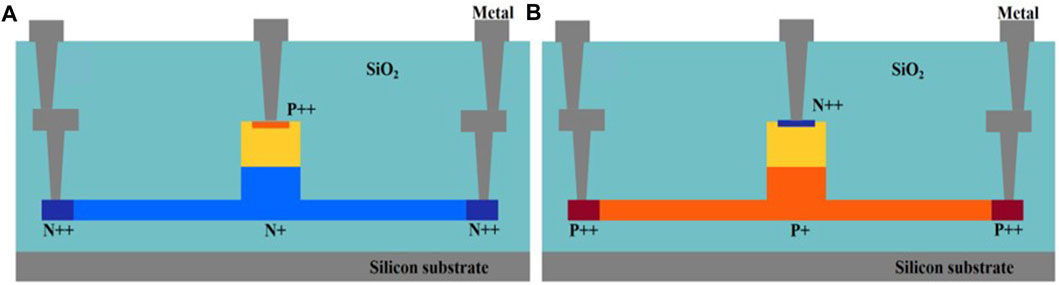
FIGURE 1. Two vertical PIN photodetector structures. (A) P-type germanium absorption layer; (B) N-type germanium absorption layer.
We also investigated the impact of carrier mobility differences in the lateral PIN junction photodetector. The cross-sectional structure of a typical lateral PIN junction photodetector is shown in Figure 2A. The slab region has a thickness of 220 nm and a length of 1.5 µm. The germanium layer is 600 nm thick, 1.5 µm wide, and 10 µm long [11]. The white region in Figure 2 represents the intrinsic silicon region with a width of 200 nm. Both the p-type and n-type silicon slab regions have a doping concentration of 1 × 1017 cm−3, while the electrode contact part is heavily doped with a concentration of 1 × 1020 cm−3 to ensure good ohmic contact [8]. To further examine the influence of the carrier transport rate on the operating frequency of the lateral PIN photodetector, additional device geometries were proposed for comparison. In Figure 2B, the length of the n-type slab is set to be 4.2 µm, which is 2.8 times that of the p-type slab, considering the disparity in carrier mobility to match the transport time of holes. Figure 2C shows the scenario where the length of the p-type slab is 2.8 times that of the n-type slab. Figure 2D presents a configuration where the length of the n-type slab is four times that of the p-type slab. For the purpose of discussion, the structures shown in Figures 2A–D are referred to as L-PIN 1, L-PIN 2, L-PIN 3, and L-PIN 4, respectively.
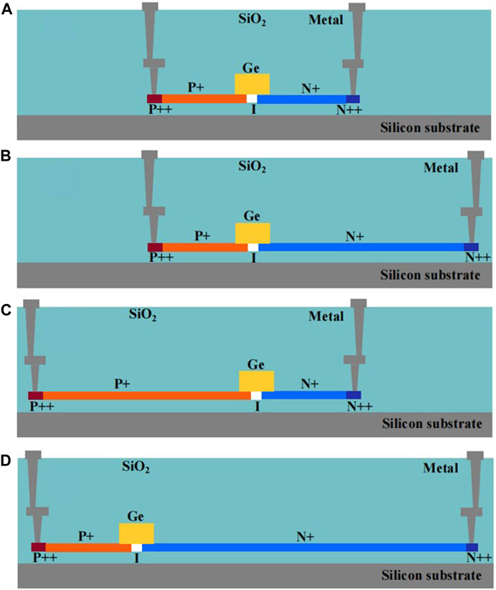
FIGURE 2. Cross-sectional diagram for four lateral PIN junction photodetectors with different slab designs. (A) The typical structure; (B) The length of the n-type slab is 2.8 times that of the p-type slab; (C) The length of the p-type slab is 2.8 times that of the n-type slab; (D) The length of the n-type slab is 4 times that of the p-type slab.
In this study, a three-dimensional finite-difference time-domain (FDTD) method is employed to simulate the propagating light field within the device structure. This simulation allows for the determination of the field distribution in the presence of the germanium layer, which is subsequently used to calculate the distribution of absorption and optical generation rate within the device. To ensure accurate results, a conformal mesh with a spatial resolution of less than 1/10 of the smallest feature size is utilized. Following the calculation of the optical generation rate, the carrier transport process is simulated. The finite element method (FEM) is employed to calculate the time-dependent carrier transport and photoresponse. A time resolution of 0.1 ps is chosen for these calculations, enabling the accurate analysis of the temporal behavior of carrier dynamics within the device. By combining the FDTD method for light-field simulation and the FEM for carrier transport and photoresponse calculations, a comprehensive understanding of the device’s performance and characteristics can be achieved.
3 Results
The photocurrent characteristics of two vertical PIN junction photodetectors, V-PIN 1 and V-PIN 2, were simulated under a bias voltage of −1 V using a 10-ps optical pulse. In Figure 3, the black curve represents V-PIN 1, while the red curve corresponds to V-PIN 2. To compare the performance of the two geometries, the photocurrent responses were normalized. In V-PIN 1, the maximum pulse current generated was 78.27, and the pulse current’s full width at half maximum (FWHM) was 19.44 ps. On the other hand, V-PIN 2 exhibited a maximum pulse current of 70.01 with a longer FWHM of 39.20 ps. This indicates that the carrier transport time in V-PIN 1 was shorter than that in V-PIN 2. The primary difference between the two vertical photodetectors lies in the doping type at the bottom of the silicon slab region. According to the Poisson equation, the electric field intensity in both vertical photodetectors and the PIN junction exceeded 104 V/cm, which is sufficiently high for the carriers in the active region to reach saturation mobility [20]. The main factor contributing to the different charge and discharge times in the two vertical photodetectors is the disparity in electron and hole mobilities in silicon. Since the carrier transport distance is much longer on the lower side of the structure, the carrier transport time in the silicon slab region becomes the limiting factor for the entire PIN junction. Notably, the carrier transport time in the n-type slab was shorter than that in the p-type slab, assuming the same doping concentration. In other words, the n-type silicon slab photodetector is capable of operating at a faster frequency due to its reduced carrier transport time.
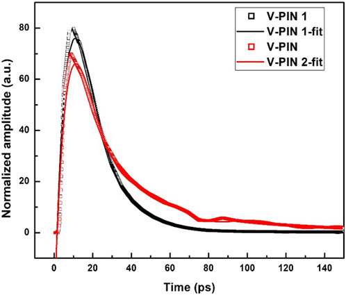
FIGURE 3. Photocurrent curve of two vertical photodetector structures under a pulsed optical signal. The square curves show the origin data, and the solid curves show the fitting results.
The frequency-dependent opto-electronic response curves of the two vertical photodetectors, V-PIN 1 and V-PIN 2, were calculated and are presented in Figure 4. In the low-frequency range, the response intensity of V-PIN 1 was higher than that of V-PIN 2. This difference can be attributed to the larger resistance in the p-type slab of V-PIN 2, leading to greater signal loss. As the frequency increased, the response intensity of V-PIN 2 began to decline noticeably at around 20 GHz, while the response intensity of V-PIN 1 started to decline at approximately 27 GHz. This observation indicates that carrier mobility has a significant influence on the charge and discharge velocity within the devices. The simulated 3-dB bandwidth for V-PIN 1 was calculated to be 42.98 GHz, while V-PIN 2 exhibited a wider bandwidth of 69.57 GHz. This difference can be attributed to the use of an n-doped silicon rib and slab structure, which demonstrated a ∼26 GHz increase in bandwidth compared to the p-doped configuration. These results highlight the importance of carrier mobility in determining the frequency response and bandwidth of the vertical photodetectors. The use of n-doped silicon structures can lead to improved performance in terms of bandwidth and high-frequency response.
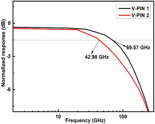
FIGURE 4. Opto-electronic response of two vertical photodetectors.
The photocurrent response curves of the four lateral PIN junction photodetectors, under a bias voltage of −1 V, were simulated and presented in Figure 5. The same 10-ps pulsed optical signal was applied to all the devices. It is worth noting that a bias voltage of −1 V was chosen to ensure that the electric field intensity in the active region of the photodetectors exceeded 104 V/cm, thus achieving saturation mobility for all carriers [20]. The photocurrent response curves of L-PIN 1 and L-PIN 2 were nearly identical, with maximum currents of 52.11 and 51.38, respectively. In contrast, the photocurrents of L-PIN 3 and L-PIN 4 exhibited significant reductions, measuring 29.53 and 34.59, respectively. The full width at half maximum (FWHM) values of the charging current curves were 25.81 ps for L-PIN 1, 25.96 ps for L-PIN 2, 45.71 ps for L-PIN 3, and 39.20 ps for L-PIN 4. The total carrier transport time remained unchanged when the length of the n-type slab was extended to 2.8 times that of the p-type slab. However, a substantial increase in carrier transport time was observed when the length of the p-type slab was extended or when the length of the n-type slab was extended to four times that of the p-type slab. It can be observed that the carrier transport time in L-PIN 1 was primarily determined by the p-type slab. When the length of the n-type slab was extended to 2.8 times that of the p-type slab, the transport time for both electrons and holes could be ideally balanced, and the carrier transport time within the PIN junction remained unaffected. Conversely, extending the length of the p-type slab resulted in a significant increase in carrier transport time, with the low hole mobility playing a decisive role. When the length of the n-type slab was extended to 4 times that of the p-type slab, the electron mobility was 2.8 times that of the hole mobility, and the transport distance was 4 times longer for electrons than for holes. As a result, electron transport took longer than hole transport, leading to an increased carrier transport time within the PIN junction. Therefore, when the length of the n-type slab is set to be 2.8 times that of the p-type slab in the lateral PIN junction Ge-on-Si photodetector, the transport time for both electrons and holes excited by light illumination within the PIN junction can be ideally matched.
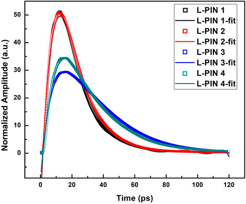
FIGURE 5. Photocurrent curve of four lateral PIN junction photodetectors. The square curves show the origin data, and the solid curves show the fitting results.
The opto-electronic bandwidth curves of the four lateral PIN junction photodetectors were simulated and are depicted in Figure 6. The 3-dB bandwidth values for L-PIN 1, L-PIN 2, L-PIN 3, and L-PIN 4 were found to be 40.86, 43.13, 28.65, and 34.73 GHz, respectively. These results are consistent with the pulse-current time characteristics observed in the PIN junctions. Notably, L-PIN 2 exhibited a larger bandwidth than L-PIN 1. The reason behind this discrepancy is that extending the length of the slab increases the distance between the two metal electrodes, resulting in a decrease in the parasitic capacitance of the electrode [21]. As a result, the loss of high-frequency signals is reduced, leading to an increase in the bandwidth. In general, extending the length of the slab tends to improve carrier transport time and resistance, which would typically reduce the bandwidth of the photodetectors. However, when the length of the n-type slab is extended to be 2.8 times that of the p-type slab, the carrier transport time is primarily determined by the p-type slab. In this case, extending the length of the n-type slab does not affect the charge and discharge time, allowing for ideal matching of the charge and discharge time between the n- and p-regions during the operation of the detectors. Although extending the length of the n-type slab may increase the resistance, the increase in resistance affects both low-frequency and high-frequency signals equally [22], thus not impacting the bandwidth. Additionally, the increase in resistance leads to a slight reduction in the voltage of the active area. However, according to the Poisson equation, the increased resistance results in a minimal decrease in electric field intensity, which still exceeds the intensity required for carriers to reach saturation mobility, while the parasitic capacitance of the electrode is reduced in L-PIN 3 and L-PIN 4 as well; its influence is relatively small compared to the increased carrier transport time, resulting in a reduction in the bandwidth of the photodetectors. The bandwidth of L-PIN 3 exhibits a significant decline starting from around 6 GHz, while the bandwidth of L-PIN 4 experiences a notable drop from approximately 8 GHz. In comparison, the bandwidth of L-PIN 1 and L-PIN 2 begins to decrease significantly after 13 GHz. The substantial decrease in response amplitude indicates that the bandwidth becomes limited by carrier mobility.
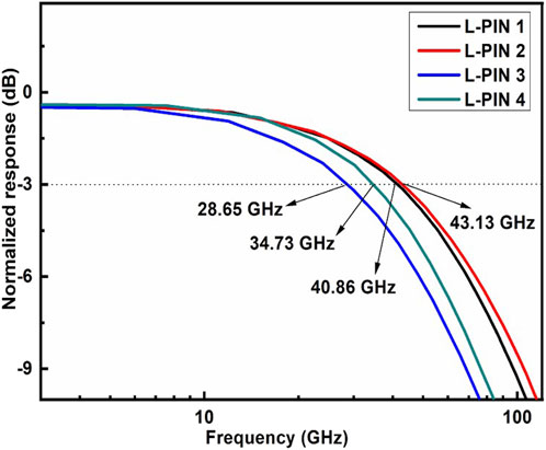
FIGURE 6. Opto-electronic response of four lateral PIN junction photodetectors.
4 Discussion
In this study, we demonstrated methods for designing both vertical and lateral PIN junction Ge-on-Si photodetectors, leveraging the mobility difference between electrons and holes. The use of an n-type doped silicon slab region resulted in a ∼26-GHz wider bandwidth for the vertical PIN junction photodetector. In lateral PIN junctions with equal lengths for the n- and p-type slabs, the charge and discharge times of the p-type region are 2.8 times longer than those of the n-type region. Consequently, the operating speed of the detector becomes restricted by the charge and discharge times of the p-type region. By extending the length of the n-type slab to 2.8 times that of the p-type slab, the charge and discharge times of both the n-type and p-type regions can be ideally matched. Additionally, the growth in the length of the n-type slab increases the distance between the electrodes, thereby reducing the parasitic capacitance. This reduction in high-frequency loss allows for an increase in the bandwidth of the photodetector.
Moreover, increasing the separation between the electrodes and the germanium absorption layer serves as an effective strategy to disrupt the confluence of bandwidth optimization and loss mitigation, a previously identified performance bottleneck. Crucially, the optimized devices can be fabricated using compatible processes available in silicon photonics foundries. The implementation of the asymmetrical slab design can be achieved using standard lithography processes. The principles and insights presented in this work offer valuable references for the design of various types and applications of active devices, making them practical and valuable for various applications in the field of optoelectronics.
Data availability statement
The original contributions presented in the study are included in the article/Supplementary Material; further inquiries can be directed to the corresponding authors.
Author contributions
CC and XX conceived the idea of the study; CC and JC conducted the simulation and analyzed the simulation data; TL and CC discussed the results and wrote the manuscript with contributions from all authors. All authors contributed to the article and approved the submitted version.
Funding
This work was supported by the National Natural Science Foundation of China (62105260), the Natural Science Foundation of Fujian Province (2021J011129 and 2020J01387), the Natural Science Basic Research Program of Shaanxi Province (2022JQ-638), the Young Talent Fund of the University Association for Science and Technology in Shaanxi, China (20220135), and the Young Talent Fund of the Xi’an Association for Science and Technology (095920221308).
Acknowledgments
The authors thank the support from the State Key Laboratory of Advanced Optical Communication Systems Networks, China.
Conflict of interest
The authors declare that the research was conducted in the absence of any commercial or financial relationships that could be construed as a potential conflict of interest.
Publisher’s note
All claims expressed in this article are solely those of the authors and do not necessarily represent those of their affiliated organizations, or those of the publisher, the editors, and the reviewers. Any product that may be evaluated in this article, or claim that may be made by its manufacturer, is not guaranteed or endorsed by the publisher.
References
1. Jalali B, Fathpour S. Silicon photonics. J Lightwave Technol (2006) 24(12):4600–15. doi:10.1109/jlt.2006.885782
2. Soref R. The past, present, and future of silicon photonics. IEEE J Sel Top Quant (2006) 12(6):1678–87. doi:10.1109/jstqe.2006.883151
3. Thomson D, Zilkie A, Bowers JE, Komljenovic T, Reed GT, Vivien L, et al. Roadmap on silicon photonics. J Optics-uk (2016) 18(7):073003. doi:10.1088/2040-8978/18/7/073003
4. Hu X, Wu D, Zhang H, Li W, Chen D, Wang L, et al. High-speed and high-power germanium photodetector with a lateral silicon nitride waveguide. Photon Res (2021) 9(5):749–56. doi:10.1364/prj.417601
5. Li X, Peng L, Liu Z, Liu X, Zheng J, Zuo Y, et al. High-power back-to-back dual-absorption germanium photodetector. Opt Lett (2020) 45(6):1358–61. doi:10.1364/ol.388011
6. Cui J, Chen H, Zhou J, Li T. High performance Ge-on-Si photodetector with optimized light field distribution by dual-injection. IEEE Photon J (2022) 14(2):1–4. doi:10.1109/jphot.2022.3153694
7. Zhang J, Lin H, Liu M, Yang Y. Research on the leakage current at sidewall of mesa Ge/Si avalanche photodiode. AIP Adv (2021) 11(7):075320. doi:10.1063/5.0054242
8. Son B, Lin Y, Lee KH, Chen Q, Tan CS. Dark current analysis of germanium-on-insulator vertical pin photodetectors with varying threading dislocation density. J Appl Phys (2020) 127(20):203105. doi:10.1063/5.0005112
9. Zuo Y, Yu Y, Zhang Y, Zhou D, Zhang X. Integrated high-power germanium photodetectors assisted by light field manipulation. Opt Lett (2019) 44(13):3338–41. doi:10.1364/ol.44.003338
10. Zhu Y, Liu Z, Niu C, Pang Y, Zhang D, Liu X, et al. High-speed and high-power germanium photodetector based on a trapezoidal absorber. Opt Lett (2022) 47(13):3263–6. doi:10.1364/ol.461673
11. Cui J, Li T, Yang F, Cui W, Chen H. The dual-injection Ge-on-Si photodetectors with high saturation power by optimizing light field distribution. Opt Commun (2021) 480:126467. doi:10.1016/j.optcom.2020.126467
12. Sproul AB, Green MA. Intrinsic carrier concentration and minority-carrier mobility of silicon from 77 to 300 K. J Appl Phys (1993) 73(3):1214–25. doi:10.1063/1.353288
13. Sun K, Costanzo R, Tzu TC, et al. Ge-on-Si waveguide photodiode array for high-power applications. In: 2018 IEEE Photonics Conference (IPC). IEEE (2018). p. 1–2.
14. De Iacovo A, Mitri F, Ballabio A, Frigerio J, Isella G, Ria A, et al. Dual-band Ge-on-Si photodetector array with custom, integrated readout electronics. IEEE Sens J (2022) 22(4):3172–80. doi:10.1109/jsen.2022.3141929
15. Alasio MGC, Goano M, Tibaldi A, et al. Bias effects on the electro-optic response of Ge-on-Si waveguide photodetectors. In: 2021 IEEE Photonics Conference (IPC). IEEE (2021). p. 1–2.
16. Li H, Zhang S, Zhang Z, Zuo S, Sun Y, et al. Silicon waveguide integrated with germanium photodetector for a photonic-integrated FBG interrogator. Nanomaterials (2020) 10(9):1683. doi:10.3390/nano10091683
17. Benedikovic D, Virot L, Aubin G, Hartmann JM, Amar F, Le Roux X, et al. Silicon–germanium receivers for short-wave-infrared optoelectronics and communications. Nanophotonics (2021) 10(3):1059–79. doi:10.1515/nanoph-2020-0547
18. Benedikovic D, Virot L, Aubin G, Baudot C, Boeuf F, Fedeli JM, et al. Comprehensive study on chip-integrated germanium pin photodetectors for energy-efficient silicon interconnects. IEEE J Quan Elect (2019) 56(1):1–9. doi:10.1109/jqe.2019.2954355
19. Li T, Nedeljkovic M, Hattasan N, Cao W, Qu Z, Littlejohns CG, et al. Ge-on-Si modulators operating at mid-infrared wavelengths up to 8 μm. Photon Res (2019) 7(8):828–36. doi:10.1364/prj.7.000828
20. Chen HT, Verheyen P, De Heyn P, Lepage G, De Coster J, Absil P, et al. High-responsivity low-voltage 28-Gb/s Ge pin photodetector with silicon contacts. J Lightwave Technol (2015) 33(4):820–4. doi:10.1109/jlt.2014.2367134
21. Kumar A, Tripathi MM, Chaujar R. Investigation of parasitic capacitances of In2O5Sn gate electrode recessed channel MOSFET for ULSI switching applications. Microsyst Technol (2017) 23(12):5867–74. doi:10.1007/s00542-017-3348-2
Keywords: silicon photonics, Ge-on-Si photodetector, PIN junction, carrier mobility, bandwidth, responsivity
Citation: Chang C, Xie X, Li T and Cui J (2023) Configuration of the active region for the Ge-on-Si photodetector based on carrier mobility. Front. Phys. 11:1150684. doi: 10.3389/fphy.2023.1150684
Received: 24 January 2023; Accepted: 05 June 2023;
Published: 20 June 2023.
Edited by:
Imran Avci, VU Amsterdam, NetherlandsReviewed by:
Junjia Wang, Southeast University, ChinaPablo Cencillo-Abad, University of Central Florida, United States
Copyright © 2023 Chang, Xie, Li and Cui. This is an open-access article distributed under the terms of the Creative Commons Attribution License (CC BY). The use, distribution or reproduction in other forums is permitted, provided the original author(s) and the copyright owner(s) are credited and that the original publication in this journal is cited, in accordance with accepted academic practice. No use, distribution or reproduction is permitted which does not comply with these terms.
*Correspondence: Xiaoping Xie, eHhwQG9wdC5hYy5jbg==; Jishi Cui, anNjdWlAZmpzbXUuZWR1LmNu