 Kamal A. Aly1,2*
 Yasser A. M. Ismail3
 Ziad Salman S. Alsulami3
 Tariq Z. Abolibda4
 Abdullah Almohammedi3
 Sobhi M. Gomha4Hoda A. Ahmed5,6Mohamed S. Ibrahim3
- 1Department of Physics, Collage of Science and Arts, Jeddah University, Jeddah, Saudi Arabia
- 2Department of Physics, Faculty of Science, Al-Azhar University, Asyut, Egypt
- 3Department of Physics, Faculty of Science, Islamic University of Madinah, Madinah, Saudi Arabia
- 4Department of Chemistry, Faculty of Science, Islamic University of Madinah, Madinah, Saudi Arabia
- 5Department of Chemistry, Faculty of Science, Cairo University, Giza, Egypt
- 6Chemistry Department, College of Sciences, Taibah University, Yanbu, Saudi Arabia
Introduction: In this study, we focus on enhancing the optical properties of PEDOT:PSS thin films by incorporating pure Sn nanoparticles (NPs) synthesized using the ultrasonic ablation technique. The objective is to investigate the impact of Sn concentration on the optical characteristics of the films, with a specific emphasis on applications in organic solar cells.
Methods: We systematically varied the concentrations of Sn in PEDOT:PSS thin films and characterized their optical properties. The index of refraction (n) and extinction coefficient (k) were precisely determined by analyzing the transmission and reflection spectra of the films. Additionally, Sellmeier’s dispersal model was employed to elucidate the obtained results of n, and dispersive factors were calculated and interpreted.
Results: The incorporation of Sn nanoparticles led to improvements in the energy bandgap (Eg) values of PEDOT:PSS films. Notably, as the concentration of Sn increased, the n values decreased, indicating enhanced suitability for organic solar cell applications. The study also unveiled a decrease in the dielectric constant of PEDOT:PSS/Sn films with increasing Sn content, resulting in improved transmittance velocity and enhanced efficacy of microelectronic devices. This, in turn, promotes the development of large-frequency and large-velocity stretchy circuit boards.
Discussion: The comprehensive assessment of optical and dielectric parameters, including complex dielectric constant, complex optical conductance, and nonlinear optical constants, provides valuable insights into the potential applications of PEDOT:PSS/Sn films. The larger nonlinear optical constants observed in the present films suggest their suitability for diverse applications such as all-optical switching, limiting, phase modulation, and frequency conversion. Overall, our findings highlight the promising potential of Sn-incorporated PEDOT:PSS thin films in advancing the field of optoelectronics and microelectronics.
1 Introduction
An important layer in different applications is the poly(3,4-ethylenedioxythiophene):poly(styrene sulfonate) (PEDOT:PSS) layer. Water-soluble PEDOT:PSS with different conductance grades can introduce good transparency in the visible region with high work function, low density, low thermal conductance, excellent thermal constancy, respectable compatibility, elasticity, and low production costs, depending on the solution [1]. Using different preparation techniques [2–6], PEDOT:PSS aqueous dispersion can easily be deposited to produce thin films with good uniformity. Otherwise, the PEDOT:PSS layer in several devices can be prepared by several simple and easy techniques at room temperature. Due to its unique properties, PEDOT:PSS is widely used in several applications, viz., different types of solar cells, organic light-emitting diodes, thermoelectric devices, electronic paper, sensors, fuel cells, carbon-capturing membranes, touch panel displays, and supercapacitors [7–14]. In solar cell applications, PEDOT:PSS is commonly used as a gap transporting plate or an electron transporting layer [7–9, 15], which can facilitate transferring charge carriers into specific electrodes.
Unfortunately, PSS moieties in the PEDOT:PSS solution are an insulator part that may deteriorate the electrical conductance of the PEDOT:PSS layer. In addition, the crystal nature of PEDOT moieties is not sufficient to encourage charge carriers to be transported through the PEDOT:PSS layer and collected by electrodes using the optoelectronic devices. Many attempts have been made to increase the electric conductance and optical transmittance of PEDOT:PSS to make them more efficient in optoelectronic devices. Among these attempts was the incorporation of organic compounds, viz., ethylene glycol (EG), methanol, ethanol, sorbitol, dimethyl sulfoxide, dimethylformamide, and fluoride surfactant, into a PEDOT:PSS aqueous solution [16–22]. The chemically functionalized multi-walled carbon nanotubes were added to the PEDOT:PSS solution to enhance the implementation of the parameters of organic solar cells [23]. Unfortunately, all previous organic compounds can impair the chemical structure of the host PEDOT:PSS solution because of the possible collaboration between the host PEDOT:PSS solution and the chemical compounds. Therefore, the physical properties (electrical conductivity and optical transparency) of PEDOT:PSS thin films can fluctuate due to the effectiveness of such chemical compounds.
The modification of the PEDOT:PSS solution by metal nanoparticle (NP) incorporation, viz., Ag, Au, and Al, is an effective approach, for improving the physical properties of PEDOT:PSS films [24]. Notarianni et al. [24] stated that Au NPs, which were introduced using the liquid chemical technique, may be incorporated into the PEDOT:PSS solution, which provides good dispersion and homogeneity in the solution. For increasing the conversion competence of organic solar cells, Woo et al. [25] prepared Au and Ag NPs using the chemical technique in the PEDOT:PSS solution through the reduction of chloroauric acid (HAuCl4) and silver nitrate (AgNO3), respectively, with a sodium borohydride (NaBH4) solution inside of the aqueous PEDOT:PSS solution. Unfortunately, metal NPs synthesized by chemical methods may have traces of the chemicals and some additives that can make a passivation layer or surfactant around the prepared NPs. The presence of such additives and chemical traces in the PEDOT:PSS solution may alter its chemical structure, and consequently, the physical properties of PEDOT:PSS thin films may be changed [26].
The improvement of the physical properties of PEDOT:PSS thin films through the incorporation of metal NPs while evading any type of chemical additions may be achieved by the generation of metal NPs in the same PEDOT:PSS solution with our promising ultrasonic ablation method [26–28], which signifies a top-down physical technique. Within this method, pure metal NPs may be formed by the effect of ultrasonic radiation on metal thin films engaged in the same PEDOT:PSS solution. Therefore, pure metal NPs may be incorporated in the PEDOT:PSS solution, avoiding the surfactants or passivation layers that may be present on the surface of the prepared NPs using chemical methods.
In the current investigation, we attempt to improve the optical parameters of PEDOT:PSS thin films by incorporating pure tin (Sn) NPs prepared using the ultrasonic ablation technique. Through this method, different Sn NP concentrations can be incorporated into the PEDOT:PSS solution, and then, PEDOT:PSS/Sn thin films can be spin coated on clean glass substrates. For determining the optical properties of PEDOT:PSS thin films, without and with different concentrations of Sn NPs, film transmittance (
2 Experimental procedures
2.1 Materials
Natural Sn shots (99.99% from Kurt J. Lesker Company Ltd., UK) were deposited onto clean glass substrates. The PEDOT:PSS solution (1.3 wt% dispersal in H2O, conductance grade with 1 S/cm conductivity) was purchased from Sigma-Aldrich and used after filtration by using a 0.22-μm PTFE filter.
2.2 Fabrication of Sn NPs in the PEDOT:PSS solution using the ultrasonic ablation method
The generation of Sn NPs inside the PEDOT:PSS solution was carried out physically using the ultrasonic ablation technique. In the beginning, a thin film of Sn metal, having a thickness of around 200 nm, was evaporated on a clean glass substrate (1 × 1 cm2) using the thermally evaporating technique (DONG, Korea) at a pressure of ∼3.8 × 10⁻⁷ torr. The PEDOT:PSS solution was filtered using a 0.22-μm PTFE filter before being used. The Sn thin film was immersed inside 1 mL of the filtered PEDOT:PSS solution in a clean glass bottle, which was dipped in an ultrasonic bath (VWR, USC-TH, Malaysia) under the effect of a frequency of 45 kHz for 30 min. For an accurate comparison, a pristine PEDOT:PSS solution (without Sn thin film) was sonicated for the same period.
2.3 Fabrication of PEDOT:PSS/Sn thin films on glass substrates
After the generation of Sn NPs inside the PEDOT:PSS solution (representing a precursor solution), different amounts or volume ratios from the precursor PEDOT:PSS solution containing Sn NPs were added to the pristine PEDOT:PSS solution. Therefore, different concentrations of Sn NPs are incorporated inside the PEDOT:PSS solution, as demonstrated in Table 1. Glass substrates having an area of 1 × 1 cm2 were ultrasonically cleaned, washed with deionized water, dried in flowing nitrogen, and then, heated in a furnace at a temperature of 373 K for 10 min. Via oxygen plasma treatment, the cleaned glass substrates were treated at 60 W for 20 min at an air-flow rate of 0.5 mbar s–1. Then, the PEDOT:PSS solution without and with different concentrations of Sn NPs was spin coated at 3,000 rpm onto cleaned and treated glass substrates following thermal annealing using a digitally controlled hot plate at 393 K for 10 min in an ambient atmosphere.
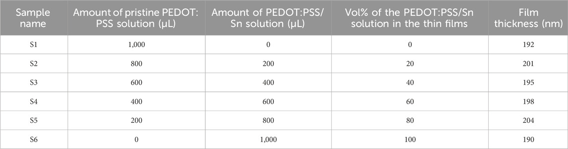
TABLE 1. Mixtures of the PEDOT:PSS/Sn solution with the pristine PEDOT:PSS solution to prepare different Sn NP concentrations incorporated into the PEDOT:PSS solution.
2.4 Measurements
The PEDOT:PSS films (∼200 nm thickness) onto glass substrates without and with different concentrations of Sn NPs were characterized using a Horiba spectroscopic ellipsometer (model Smart-SE, USA) by measuring the refractive index and the extinction coefficient by investigating the film thickness. Furthermore, the films thicknesses were assured using Tolansky’s interferometric technique [29]. The film transmittance and reflectance were measured in the 0.2–2.5 μm wavelength range using a Jasco-630 V double-beam spectrometer. The resistivity and sheet resistance of the PEDOT:PSS films with and without Sn NPs were measured by the Hall Effect setup at room temperature using a system from MMR technologies Inc. including the digital Hall Effect controller H5000 and digital temperature controller K2000.
3 Results and discussion
The shape of Sn nanoparticles, which were generated in the PEDOT:PSS solution, can be illustrated through SEM images, as shown in Figure 1 for samples numbers 2 and 3. From the SEM images of PEDOT:PSS/Sn films, it can be observed that Sn NPs are just physically suspended and spread over the PEDOT:PSS film, without interaction (chemically) with the matrix of the PEDOT:PSS film. Figure 1 shows that Sn NPs can be generated in the PEDOT:PSS solution with varying sizes influenced by ultrasonic power and the acidic nature of the PEDOT:PSS solution. Moreover, sizable Sn pieces are observable in the PEDOT:PSS/Sn films. From the SEM images of the Sn NPs embedded in PEDOT:PSS films in Figure 1 for samples S2 and S3, it appears that there is a wide distribution in NP sizes.
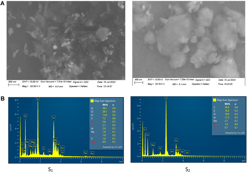
FIGURE 1. (A) SEM images and (B) EDS mapping and elemental distribution for S2 and S3 samples.
Figure 2 shows the
where constants a and b are given in the same figure. The stationary or static refractive index (
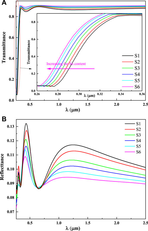
FIGURE 2. (A) T vs. λ and (B) R vs. λ for S1–S6 films.
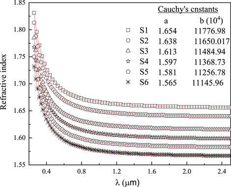
FIGURE 3.
3.1 Dispersion parameters
According to the simple dispersion model suggested by Sellmeier, in the low absorption range, the index of refraction n of a dielectric medium can be written as follows [37]:
where
Both
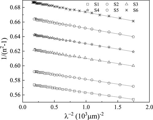
FIGURE 4. Slimmer’s figure for S1–S6 films.
The evaluated
TABLE 2. Optical constants for different Sn NP concentrations incorporated into the PEDOT:PSS solution.
The optical moments,
We can compute
The estimated values of
3.1.1 Absorbance coefficient and optical band gap
The excellence and evidence of thin films, including their concentrations, surface properties, and suitability, are demonstrated by the absorbance value (
where
where n represents the film’s refractive index,
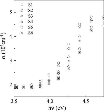
FIGURE 5.
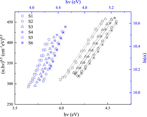
FIGURE 6.
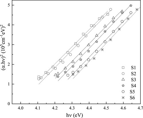
FIGURE 7. (αhν)2 and ln(α) vs. hν for S1–S6 films.
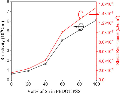
FIGURE 8. Resistivity and sheet resistance vs. Sn contents for S1–S6 films.
In the region of low absorption, the absorption coefficient shows an exponential dependence on photon energy,
where
3.1.2 Dielectric optical constants
When determining whether a material is suitable for optoelectronic devices, the dielectric constant is a key consideration [31, 49]. The polarizability of materials and the dielectric constant are correlated in the optical domain. The values of the energy loss function, polarizabilities, dissipation parameter, and dielectric loss are only a few examples of variables whose information is usefully provided by the dielectric constant. Both the real and imaginary parts (
The real part,
Figures 9, 10 show how
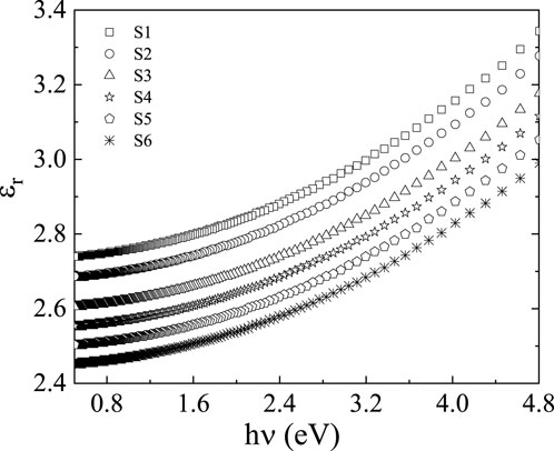
FIGURE 9.
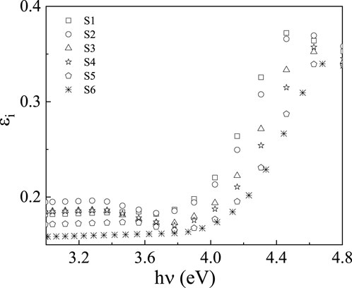
FIGURE 10.
Complex optical conductivity (
The imaginary portion of optical conductivity,
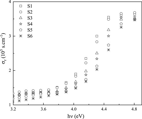
FIGURE 11.
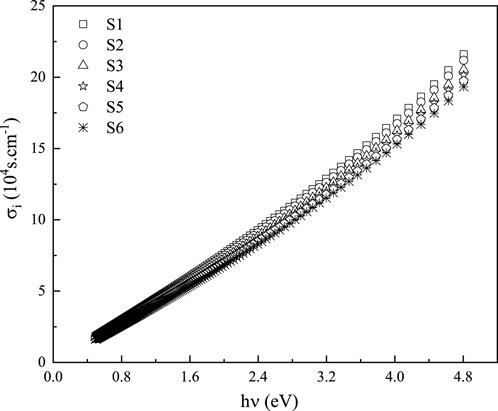
FIGURE 12.
3.2 Optical nonlinearity
The electric field effect on the nonlinear refractive index is linked to the high-order susceptibility and may be written as
where
The calculated values of
4 Conclusion
The incorporation of Sn NPs inside PEDOT:PSS thin films was successfully performed through an innovative ultrasonic ablation technique. Using the measured film transmission and reflection spectra, the refractive index (
Data availability statement
The raw data supporting the conclusions of this article will be made available by the authors, without undue reservation.
Author contributions
KA: methodology, resources, software, and writing–original draft. YI: data curation, funding acquisition, project administration, and writing–review and editing. ZS: conceptualization, formal analysis, investigation, visualization, and writing–original draft. TA: investigation, resources, supervision, and writing–original draft. AA: formal analysis, methodology, software, and writing–original draft. SG: formal analysis, investigation, resources, validation, and writing–review and editing. HA: conceptualization, supervision, validation, visualization, and writing–review and editing. MI: investigation, supervision, visualization, and writing–review and editing.
Funding
The authors declare that financial support was received for the research, authorship, and/or publication of this article. This work was financially supported by the Deanship of Scientific Research in the Islamic University of Madinah, Saudi Arabia [The Research Groups Grant (First Call): Number 945].
Conflict of interest
The authors declare that the research was conducted in the absence of any commercial or financial relationships that could be construed as a potential conflict of interest.
Publisher’s note
All claims expressed in this article are solely those of the authors and do not necessarily represent those of their affiliated organizations, or those of the publisher, the editors, and the reviewers. Any product that may be evaluated in this article, or claim that may be made by its manufacturer, is not guaranteed or endorsed by the publisher.
References
1. Zhu Z, Liu C, Jiang F, Xu J, Liu E. Effective treatment methods on PEDOT:PSS to enhance its thermoelectric performance. Synth Met (2017) 225:31–40. doi:10.1016/j.synthmet.2016.11.011
2. Kim G-E, Shin D-K, Lee J-Y, Park J. Effect of surface morphology of slot-die heads on roll-to-roll coatings of fine PEDOT:PSS stripes. Org Elect (2019) 66:116–25. doi:10.1016/j.orgel.2018.12.033
3. Koidis C, Logothetidis S, Kapnopoulos C, Karagiannidis PG, Laskarakis A, Hastas NA. Substrate treatment and drying conditions effect on the properties of roll-to-roll gravure printed PEDOT:PSS thin films. Mater Sci Eng B (2011) 176:1556–61. doi:10.1016/j.mseb.2011.03.007
4. Griffin J, Ryan AJ, Lidzey DG. Solution modification of PEDOT:PSS inks for ultrasonic spray coating. Org Elect (2017) 41:245–50. doi:10.1016/j.orgel.2016.11.011
5. Kim B-J, Han S-H, Park J-S. Properties of CNTs coated by PEDOT:PSS films via spin-coating and electrophoretic deposition methods for flexible transparent electrodes. Surf Coat Tech (2015) 271:22–6. doi:10.1016/j.surfcoat.2015.01.045
6. Zabihi F, Xie Y, Gao S, Eslamian M. Morphology, conductivity, and wetting characteristics of PEDOT:PSS thin films deposited by spin and spray coating. Appl Surf Sci (2015) 338:163–77. doi:10.1016/j.apsusc.2015.02.128
7. Arora S, Singh V, Arora M, Pal Tandon R. Evaluating effect of surface state density at the interfaces in degraded bulk heterojunction organic solar cell. Physica B: Condensed Matter (2012) 407:3044–6. doi:10.1016/j.physb.2011.08.086
8. Singh V, Arora S, Arora M, Sharma V, Tandon RP. Characterization of doped PEDOT: PSS and its influence on the performance and degradation of organic solar cells. Semiconductor Sci Tech (2014) 29. doi:10.1088/0268-1242/29/4/045020
9. Sun K, Zhang S, Li P, Xia Y, Zhang X, Du D, et al. Review on application of PEDOTs and PEDOT:PSS in energy conversion and storage devices. J Mater Sci Mater Elect (2015) 26:4438–62. doi:10.1007/s10854-015-2895-5
10. Lee JH, Jung JP, Jang E, Lee KB, Hwang YJ, Min BK, et al. PEDOT-PSS embedded comb copolymer membranes with improved CO2 capture. J Membr Sci (2016) 518:21–30. doi:10.1016/j.memsci.2016.06.025
11. Meng Y, Ahmadi M, Wu X, Xu T, Xu L, Xiong Z, et al. High performance and stable all-inorganic perovskite light emitting diodes by reducing luminescence quenching at PEDOT:PSS/Perovskites interface. Org Elect (2019) 64:47–53. doi:10.1016/j.orgel.2018.10.014
12. Meng Q, Jiang Q, Cai K, Chen L. Preparation and thermoelectric properties of PEDOT:PSS coated Te nanorod/PEDOT:PSS composite films. Org Elect (2019) 64:79–85. doi:10.1016/j.orgel.2018.10.010
13. Baruah B, Kumar A. PEDOT:PSS/MnO2/rGO ternary nanocomposite based anode catalyst for enhanced electrocatalytic activity of methanol oxidation for direct methanol fuel cell. Synth Met (2018) 245:74–86. doi:10.1016/j.synthmet.2018.08.009
14. Singh SB, Kshetri T, Singh TI, Kim NH, Lee JH. Embedded PEDOT:PSS/AgNFs network flexible transparent electrode for solid-state supercapacitor. Chem Eng J (2019) 359:197–207. doi:10.1016/j.cej.2018.11.160
15. Sarker AK, Kim J, Wee B-H, Song H-J, Lee Y, Hong J-D, et al. Hydroiodic acid treated PEDOT:PSS thin film as transparent electrode: an approach towards ITO free organic photovoltaics. RSC Adv (2015) 5:52019–25. doi:10.1039/c5ra07136d
16. Alemu D, Wei H-Y, Ho K-C, Chu C-W. Highly conductive PEDOT:PSS electrode by simple film treatment with methanol for ITO-free polymer solar cells. Energ Environ Sci (2012) 5:9662–71. doi:10.1039/c2ee22595f
17. Kim JY, Jung JH, Lee DE, Joo J. Enhancement of electrical conductivity of poly(3,4-ethylenedioxythiophene)/poly(4-styrenesulfonate) by a change of solvents. Synth Met (2002) 126:311–6. doi:10.1016/s0379-6779(01)00576-8
18. Huang J, Miller PF, Wilson JS, de Mello AJ, de Mello JC, Bradley DDC. Investigation of the effects of doping and post-deposition treatments on the conductivity, morphology, and work function of poly(3,4-ethylenedioxythiophene)/poly(styrene sulfonate) films. Adv Funct Mater (2005) 15:290–6. doi:10.1002/adfm.200400073
19. Zhou Y, Cheun H, Choi S, Potscavage WJ, Fuentes-Hernandez C, Kippelen B. Indium tin oxide-free and metal-free semitransparent organic solar cells. Appl Phys Lett (2010) 97:153304. doi:10.1063/1.3499299
20. Badre C, Marquant L, Alsayed AM, Hough LA. Highly conductive poly(3,4-ethylenedioxythiophene):poly (styrenesulfonate) films using 1-Ethyl-3-methylimidazolium tetracyanoborate ionic liquid. Adv Funct Mater (2012) 22:2723–7. doi:10.1002/adfm.201200225
21. Vosgueritchian M, Lipomi DJ, Bao Z. Highly conductive and transparent PEDOT:PSS films with a fluorosurfactant for stretchable and flexible transparent electrodes. Adv Funct Mater (2012) 22:421–8. doi:10.1002/adfm.201101775
22. Ko C-J, Lin Y-K, Chen F-C, Chu C-W. Modified buffer layers for polymer photovoltaic devices. Appl Phys Lett (2007) 90:063509. doi:10.1063/1.2437703
23. Lee I, Lee S, Kim H, LeeKim HY. Polymer solar cells with polymer/carbon nanotube composite hole-collecting buffer layers. Open Phys Chem J (2010) 4:1–3. doi:10.2174/1874067701004010001
24. Notarianni M, Vernon K, Chou A, Aljada M, Liu J, Motta N. Plasmonic effect of gold nanoparticles in organic solar cells. Solar Energy (2014) 106:23–37. doi:10.1016/j.solener.2013.09.026
25. Woo S, Jeong JH, Lyu HK, Han YS, Kim Y. In situ-prepared composite materials of PEDOT: PSS buffer layer-metal nanoparticles and their application to organic solar cells. Nanoscale Res Lett (2012) 7:641. doi:10.1186/1556-276x-7-641
26. Ismail YAM, Kishi N, Soga T. Ultrasonic ablation as a novel technique for producing pure aluminium nanoparticles dispersed in different liquids for different applications. Jpn J Appl Phys (2015) 54:075002. doi:10.7567/jjap.54.075002
27. Ismail YAM, Kishi N, Soga T. Improvement of organic solar cells using aluminium microstructures prepared in PEDOT:PSS buffer layer by using ultrasonic ablation technique. Thin Solid Films (2016) 616:73–9. doi:10.1016/j.tsf.2016.08.001
28. Ismail YAM. Aluminium nanoparticles prepared by ultrasonic ablation technique inside the active layer of organic solar cell. J Nano Res (2018) 51:48–60. doi:10.4028/www.scientific.net/jnanor.51.48
29. Tolansky S, Omar M. Thin-film interferometric techniques for high-magnification topographical studies. Nature (1952) 170:81–2. doi:10.1038/170081b0
30. Hassanien AS, Akl AA. Influence of composition on optical and dispersion parameters of thermally evaporated non-crystalline Cd50S50−xSex thin films. J Alloys Comp (2015) 648:280–90. doi:10.1016/j.jallcom.2015.06.231
31. Hassanien AS, Sharma I. Dielectric properties, Optoelectrical parameters and electronic polarizability of thermally evaporated a-Pb-Se-Ge thin films. Physica B: Condensed Matter (2021) 622:413330. doi:10.1016/j.physb.2021.413330
32. Hassanien AS, Sharma I, Aly KA. Linear and nonlinear optical studies of thermally evaporated chalcogenide a-Pb-Se-Ge thin films. Physica B: Condensed Matter (2021) 613:412985. doi:10.1016/j.physb.2021.412985
33. Murmann H. Der spektrale Verlauf der anomalen optischen Konstanten dünnen Silbers. Z für Physik (1936) 101:643–8. doi:10.1007/BF01349608
35. Ibraheem AA, Aly KA. Optical and dispersion parameters of Ge-Zn-Se glassy films for VIS and FTIR Applications. Physica Scripta (2023) 98:015810. doi:10.1088/1402-4896/aca630
36. Aly KA, Afify N, Abousehlly AM, Abd Elnaeim AM. Optical band gap and refractive index dispersion parameters of In–Se–Te amorphous films. J Non-Crystalline Sol (2011) 357:2029–34. doi:10.1016/j.jnoncrysol.2011.02.032
37. DrDomenico M, Wemple SH. Oxygen-octahedra ferroelectrics. I. Theory of electro-optical and nonlinear optical effects. J Appl Phys (2003) 40:720–34. doi:10.1063/1.1657458
38. Aly KA. Comment on the relationship between electrical and optical conductivity used in several recent papers published in the journal of materials science: materials in electronics. J Mater Sci Mater Elect (2022) 33:2889–98. doi:10.1007/s10854-021-07496-9
39. Kumar A, Ali V, Kumar S, Husain M. Studies on conductivity and optical properties of poly(o-toluidine)-ferrous sulfate composites. Int J Polym Anal Characterization (2011) 16:298–306. doi:10.1080/1023666x.2011.587945
40. Sharda S, Sharma E, Aly KA, Dahshan A, Sharma P. High refractive index (Dy) doped (GeTe2)80(In2Te3)20 thin films for sub-THz and millimeter-wave applications. Ceramics Int (2021) 47:34501–7. doi:10.1016/j.ceramint.2021.08.364
41. Minkov D, Vateva E, Skordeva E, Arsova D, Nikiforova M. Optical properties of Ge-As-S thin films. J Non-Crystalline Sol (1987) 90:481–4. doi:10.1016/s0022-3093(87)80469-6
42. Rafea MA, Farag AAM, Roushdy N. Structural and optical characteristics of nano-sized structure of Zn0.5Cd0.5S thin films prepared by dip-coating method. J Alloys Comp (2009) 485:660–6. doi:10.1016/j.jallcom.2009.06.048
43. Hassanien AS, Aly KA, Akl AA. Study of optical properties of thermally evaporated ZnSe thin films annealed at different pulsed laser powers. J Alloys Comp (2016) 685:733–42. doi:10.1016/j.jallcom.2016.06.180
44. Hegazy HH, Dahshan A, Aly KA. Influence of Cu content on physical characterization and optical properties of new amorphous Ge–Se–Sb–Cu thin films. Mater Res Express (2019) 6:025204. doi:10.1088/2053-1591/aaee4b
45. Tauc J, Menth A. States in the gap. J Non-Crystalline Sol (1972) 8-10:569–85. doi:10.1016/0022-3093(72)90194-9
46. Davis EA, Mott NF. Conduction in non-crystalline systems V. Conductivity, optical absorption and photoconductivity in amorphous semiconductors. Phil Mag A J Theor Exp Appl Phys (1970) 22:0903–22. doi:10.1080/14786437008221061
47. Ibraheem AA, Aly KA. Physical characterization of Ge–Zn–Se thin films. J Mater Sci Mater Elect (2022) 33:26905–14. doi:10.1007/s10854-022-09355-7
48. Urbach F. The long-wavelength edge of photographic sensitivity and of the electronic absorption of solids. Phys Rev (1953) 92:1324. doi:10.1103/physrev.92.1324
49. Aly KA. Optical constants of quaternary Ge-As-Te-In amorphous thin films evaluated from their reflectance spectra. Phil Mag (2009) 89:1063–79. doi:10.1080/14786430902870542
50. Shen Q, Ayuzawa Y, Katayama K, Sawada T, Toyoda T. Separation of ultrafast photoexcited electron and hole dynamics in CdSe quantum dots adsorbed onto nanostructured TiO2 films. Appl Phys Lett (2010) 97:263113. doi:10.1063/1.3533374
51. Farag AAM, Yahia IS. Structural, absorption and optical dispersion characteristics of rhodamine B thin films prepared by drop casting technique. Opt Commun (2010) 283:4310–7. doi:10.1016/j.optcom.2010.06.081
52. Liu Y, Zhao X-Y, Sun Y-G, Li W-Z, Zhang X-S, Luan J. Synthesis and applications of low dielectric polyimide. Resour Chemicals Mater (2023) 2:49–62. doi:10.1016/j.recm.2022.08.001
53. Sharma I, Sharma P, Hassanien AS. Optical properties and optoelectrical parameters of the quaternary chalcogenide amorphous Ge15SnxS35-xTe50 films. J Non-Crystalline Sol (2022) 590:121673. doi:10.1016/j.jnoncrysol.2022.121673
54. Sharda S, Sharma E, Aly KA, Dahshan A, Sharma P. Thermo-induced changes in the optical linearity and nonlinearity of Dy doped (GeSe2)80(Sb2Se3)20 thin films. Opt Quan Elect (2022) 54:249. doi:10.1007/s11082-022-03653-4
55. Hassanien AS. Studies on dielectric properties, opto-electrical parameters and electronic polarizability of thermally evaporated amorphous Cd50S50−xSex thin films. J Alloys Comp (2016) 671:566–78. doi:10.1016/j.jallcom.2016.02.126
56. El-Nahass MM, Farid AM, Atta AA. Structural and optical properties of Tris(8-hydroxyquinoline) aluminum (III) (Alq3) thermal evaporated thin films. J Alloys Comp (2010) 507:112–9. doi:10.1016/j.jallcom.2010.07.110
57. Tanaka K. Optical nonlinearity in photonic glasses. J Mater Sci Mater Elect (2005) 16:633–43. doi:10.1007/s10854-005-3738-6
58. Dimitrov V, Sakka S. Linear and nonlinear optical properties of simple oxides. II. J Appl Phys (1996) 79:1741–5. doi:10.1063/1.360963
59. Tichá H, Tichý L. Semiempirical relation between non-linear susceptibility (refractive index), linear refractive index and optical gap and its application to amorphous chalcogenides. J Optoelectronics Adv Mater (2002) 4:381–6.
60. Boyd RW. Chapter 6 - nonlinear Optics in the two-level approximation. In: RW Boyd, editor. Nonlinear Optics. 3rd ed. Burlington: Academic Press (2008). p. 277–328.
Keywords: organic solar cells, Sn nanoparticles, optical properties of thin films, dielectrics, PEDOT:PSS thin film
Citation: Aly KA, Ismail YAM, Salman S. Alsulami Z, Abolibda TZ, Almohammedi A, Gomha SM, Ahmed HA and Ibrahim MS (2024) Effect of Sn nanoparticles on the optical properties of PEDOT:PSS thin films. Front. Phys. 12:1331133. doi: 10.3389/fphy.2024.1331133
Received: 31 October 2023; Accepted: 08 February 2024;
Published: 05 March 2024.
Edited by:
Bożena Jarząbek, Polish Academy of Sciences, PolandCopyright © 2024 Aly, Ismail, Salman S. Alsulami, Abolibda, Almohammedi, Gomha, Ahmed and Ibrahim. This is an open-access article distributed under the terms of the Creative Commons Attribution License (CC BY). The use, distribution or reproduction in other forums is permitted, provided the original author(s) and the copyright owner(s) are credited and that the original publication in this journal is cited, in accordance with accepted academic practice. No use, distribution or reproduction is permitted which does not comply with these terms.
*Correspondence: Kamal A. Aly, a2FhbGk1QHVqLmVkdS5zYQ==