 Jinxi Bai
 Huan Ren
- Laser Fusion Research Center, China Academy of Engineering Physics, Mianyang, China
A wide-field high resolution microscopy with sub-micron resolution and high contrast image was demonstrated by using the isotropy frequency-domain extension imaging (IFEI), which was successfully applied to submicron-scale structure detection of fused silica wafer for the first time. Employing the frequency-domain extension and the isotropic period matching, the IFEI extended the bandwidth of coherent transfer function of the conventional wide-field microscopy, thereby improving the resolution to break the diffraction limit. In this method, a quantitative measurement of 200 nm was achieved using fused silica wafer with prefabricated etched structure on the surface. By imaging 81 nm gold nanoparticles, the system resolution calibration was achieved. And corresponding system’s lateral resolution of approximately 179.5 nm was obtained, which was 1.72 times higher than the conventional wide-field microscopy image. Moreover, the reconstructed IFEI images of ultra-precision processed fused silica optics were demonstrated to present the finer structures of sub-micron digs and scratches formed in the optics manufacturing process.
Introduction
Fused silica material is widely used in high-energy laser, space detection, remote sensing imaging, biomedical microscopic imaging and other fields due to its outstanding optical properties. In high-energy laser devices, the demand for fused silica material is extremely large, but laser-induced damage is prone to occur under high throughput conditions, which has become one of the key issues restricting the further increase of the throughput of the high-energy laser system [1, 2]. The existing studies have shown that defects (sub-micron to tens of micron scale lateral dimensions defects, and surface cracks) generated during the manufacturing process are the natural source of the decreasing of laser-induced damage threshold of fused silica optics [3–7]. With the rapid development of precision manufacturing technology for optical components, effective control of defects above several micrometers has been achieved, and corresponding the damage threshold of optical elements has been greatly improved. However, it is still about an order of magnitude lower than the intrinsic threshold of materials, so the high damage threshold defects at the sub-micron scale have become a key limiting factor for further improvement of the damage resistance of fused silica optics [8, 9]. How to effectively suppress sub-micron defects has become an important scientific problem in the fields of precision manufacturing and laser damage resistance.
If you want to suppress or eliminate it, the first rule is to find it. At present, the methods for characterizing surface defects of fused silica optics mainly include optical microscopy, optical scattering [9, 10], interference [11], laser confocal microscopy (LCM) [12, 13], scanning probe-based microscopy (SPM) [14], atomic force microscope (AFM) [3, 15] and scanning electron microscope (SEM) [3, 15]. Limited by the Abbe-Rayleigh diffraction limit, microscopy and optical scattering methods can only achieve defect detection within a certain range of scales (>λ/2) [16, 17], and just can obtain two-dimensional morphological information of defects. AFM and SPM with high spatial resolution can obtain three-dimensional topography of defect space, but the detection efficiency is extremely low, and the work distance is ultra-short. Therefore it is extremely difficult to apply to the detection of fused silica optics. SEM is major applied in the surface morphology detection of conducting materials. The optical components usually need to be treated with gold spraying and other methods, which will cause intrusive pollution and is almost repulsive for precision optics. Although LCM uses a specially modulated incident light to obtain a smaller focused spot size, its improvement process depends entirely on the wavelength of the illumination laser and the numerical aperture of the microscope objective lens. It cannot break the diffraction limit and the detection method based on point-by-point scanning stitching imaging has low detection efficiency for optical elements. Consequently, the shortcomings of existing detection methods directly limit further improvement of the precision manufacturing level of fused silica optics, which affects the suppression of effects and the upgrading of surface processing technology. Therefore, we aim to investigate a high resolution imaging technology which is suitable for sub-micron scale defect detection of fused silica optics.
On the other hand, many attempts to break the diffraction limit and achieve super-resolution have achieved great success in fluorescent imaging. These super-resolution techniques such as stimulated emission depletion (STED) [18, 19], fourier ptychographic microscopy (FPM) [20, 21], structured illumination microscopy (SIM) [22, 23], stochastic optical reconstruction microscopy (STORM) [24] and photoactivated localization microscopy (PALM) [25], have been developed based on structure pattern illumination or single molecular location. However, most of these super-resolution techniques need to be combined with fluorescence processing to achieve super-resolution microscopic imaging, which are mainly applied in the biomedical field. And only frequency-domain extension super-resolution imaging has been developed into the non-fluorescent field [22, 23, 26–31], which does not require fluorescent treatment of the test sample, and has a fast imaging speed with wide imaging field, but when observing the phase sample without any processing, the imaging contrast is low, and often requires the use of gold nanoparticles and differential interference contrast module to assist imaging, or needs to have contrast samples to achieve high-contrast imaging make them poorly suited for transparent phase sample. Therefore, we have comprehensively transformed the optical path and high-resolution reconstruction algorithm of the traditional frequency-domain extension high-resolution imaging system. While greatly improving the imaging quality of the system and reducing the size of the optical path, we have solved the problem of weak imaging contrast for transparent optical components. It provides an effective method for the detection of micro-nano defects on the surface of optical components.
In this work, we propose a wide-field high resolution microscopy by using the isotropy frequency-domain extension imaging (IFEI), which is capable to provide high resolution and high contrast images with sub-micron scale defects on the surface of fused silica optics for the first time. With 0.8 numerical aperture dry objective at 405 nm, an accurate high resolution imaging of the 200 nm scratch and dig defects was achieved based on the fused silica wafer. Furthermore, the system resolution calibration was demonstrate by imaging 81 nm gold nanoparticles, and the system’s lateral resolution was approximately 179.5 nm, which was 1.72 times higher than the conventional wide-field (WF) microscopy image [16, 17].
Theory and experimental setup of isotropy frequency-domain extension imaging
Theoretical foundation of isotropy frequency-domain extension imaging
Isotropy frequency-domain extension imaging (IFEI) is also called frequency domain processing technology. The basic principle is that utilizing moiré fringe moves high-frequency information that could not pass through the system to the spectral region detectable by the optical imaging system. However, the high-frequency information limit collected by the detector is mixed with the smaller frequency information of the sample due to the frequency shift, which is difficult to distinguish directly. The post-processing of data is required to complete the separation of high-frequency information and move to the correct position in order to improve resolution. To achieve an isotropic increase of resolutions of samples, multi-directional and multi-phase sinusoidal structured light illumination is currently used (Figure 1A) [32, 33].
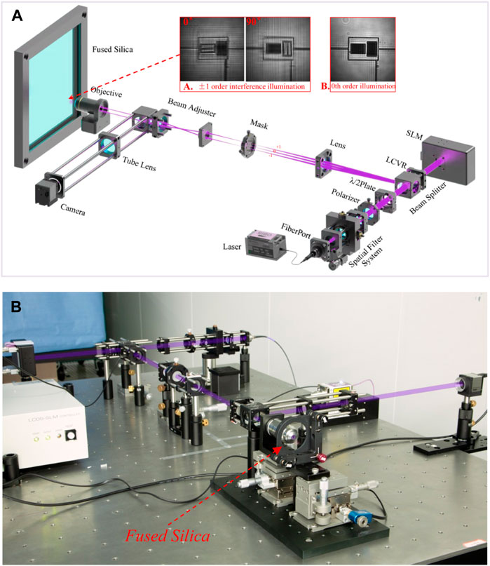
FIGURE 1. (A) Principle diagram and (B) experimental setup for the IFEI system.
More specifically, the spectral distribution of the sinusoidal function is exactly three impulse response functions (
The intensity of sinusoidal illumination
Where
In general, assuming that the intensity of the emission light
The observed information by the detector can be described as a convolution of the intensity of the emission light and the point spread function (PSF) of the optical microscopy system.
Where
To simplify the operation and better understand IFEI theorem, discussions in the frequency domain is recommend for the detected information. The Fourier transform of Eq.3 can be written as
Where
In order to adequately extract those two parts of new observable information, we use three structured pattern with different phases to illuminate the sample. By using the images acquired by the detector, the following matrix equation can be constructed.
By solving
Experimental setup of isotropy frequency-domain extension imaging
The schematic diagram of a 2D IFEI system is shown in Figure 1. The IFEI used ±1 diffraction order interference to generate multiple angles patterned illumination and it was totally home-built instead of building around a commercial microscope. In order to obtain optimal image contrast, a Gaussian single mode coherent laser (Coherent, OBIS FP 405LX) was used as a light source. The fiber port collimator and the custom designed precision spatial filter system were placed behind the laser to obtain the uniform and collimated Gaussian beam. Then, a polarizer and a λ/2 plate combined with liquid crystal variable retarder (LCVR, Thorlabs, LCR1-405-SP) were used. The polarization state of the laser incident on the spatial light modulator (SLM, X13138-01, Hamamatsu) was parallel to the periodic grating pattern loaded on the SLM in synchronization to get a high contrast of illumination pattern onto the specimen. A cube-mounted polarization-insensitive beam-splitter and a variable aperture slot were need to transmit the diffraction orders generated by the SLM, and the laser beam filled the active surface of the SLM, which made the SLM work at an optimal first-order diffraction efficiency. Afterwards, the diffracted orders from the SLM were focused by an aspheric lens, and a spatial mask was inserted at the focal plane of the aspheric lens to get rid of the zero order and other undesired diffracted orders. And only two ±1 order beams were focused and de-magnifies onto the back focal plane of the objective (TU Plan EPI ELWD ×100/0.8, Nikon) at positions near the opposite edges to form the illumination period near the diffraction limit via the beam adjuster. And then, the desired two beamlets interfered each other at the focal plane of the objective, forming a sinusoidal illumination pattern (Figure 1A) to achieve moiré modulation on the detection target. The fused silica sample was fixed on a precision 3D motorized translation stage with a piezoelectric actuator (Picomotor SNM01, Shinopto Inc.) with a minimum step of 30 nm to replace Z-axis for accurate focusing of the sample. A USB 3.0 CCD camera (Thorlabs, DCU224M, 8-bits, 1,280 × 1,024 pixels with pixel size of 4.65 × 4.65μm2) was employed to collect the reflected and scattered light with a tube lens. The focal length of the tube lens was 250 mm, combined with the 100×/0.8 objective, giving a total magnification of ×129.5, corresponding to a single pixel size of 35.9 nm at the sample plane of our IFEI system. Finally, six individual images were used to reconstruct a high-resolution output image, which were acquired with two different illumination patterns (0°, 90°) at three separate phases (0°, 120°, 240°) for each pattern loaded on the SLM. Figure 1B is the diagram of the experimental setup we built according to the principle diagram of Figure 1A. The full cage structures and compact modular design ensure that the high resolution imaging system has excellent resistance to environment interference, while greatly reducing the volume of the optical path with excellent engineering application capabilities.
Experimental results and discussions
Imaging verification of fused silica surface defects
To evaluate our self-developed IFEI system for defects detection of fused silica optics, a customized optical elements (COE) was chosen as the test sample (Figure 2A). As we all know that the surface defects of fused silica are mainly divided into scratch defects and dig defects. Therefore, we prefabricated scratch defects and dig defects in standard sizes on the surface of COE, and achieved dimension calibration of etching defects by SEM. The prefabricated defects are located in a 200 μm rectangular area in the center of the COE (the red dot in Figure 2A), and the specific distribution is show in Figure 2B. It is obvious that the defects mainly composed of eight groups of scratches with different widths and eight types of digs with different diameters. The scratch linewidths (or the dig diameters) from large to small were 1 μM, 0.5 μM, 0.4 μM, 0.3 μM, 0.25 μM, 0.2 μM, 0.15 μM, and 0.1 μM, respectively. Among them, the gap width of each etching line for scratch defects was equal to the linewidth. We mainly compared the resolution achieved between the wide-field and reconstructed IFEI image of the sixth group of scratches structures (0.2 μM line width) and digs (0.2 μM diameters) on the COE.
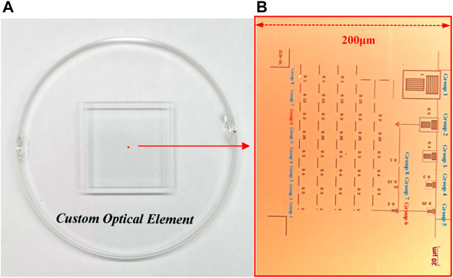
FIGURE 2. (A) Image of the COE. (B) Full field of view image of the test target on the COE.
Figures 3A,B represent the image of the sixth group of scratch structures using SEM. It can be seen from Figure 3B that the minimum width of scratch defects was ∼173.1nm, and the average width of the scratch defects was ∼203 nm. Figure 3C is the conventional wide-field image as a contrast, which was obtained by using the 0th order diffraction light as a uniform illumination light source based on IFEI system (Figure 1A). Compared with Figure 3D, which was clearly imaged after IFEI reconstruction, the ∼200 nm scratch structure was far beyond the resolution limit of the wide-field microscope (δ = 0.61 405nm/0.8 = 308.8 nm). For a more characteristic analysis, Figure 3E,F show the intensity distribution of scratch structure defects in the horizontal and vertical cross sections at the dashed lines in Figures 3C,D. It is observed that the peak-to-valley ratio (VPR) in both directions of the wide-field image was basically equal to 1, which did not have the ability to resolve 0.2 μM scratch structure defects. And the intensity distributions of VPR in both directions of the resolution enhanced image was less than 0.45, which satisfied the resolution definitions [38]. In other words, 0.2 μM scratch structure defects of fused silica can be clearly resolved by using the conventional 100×/0.8 objective at the wavelength of 405 nm in IFEI.
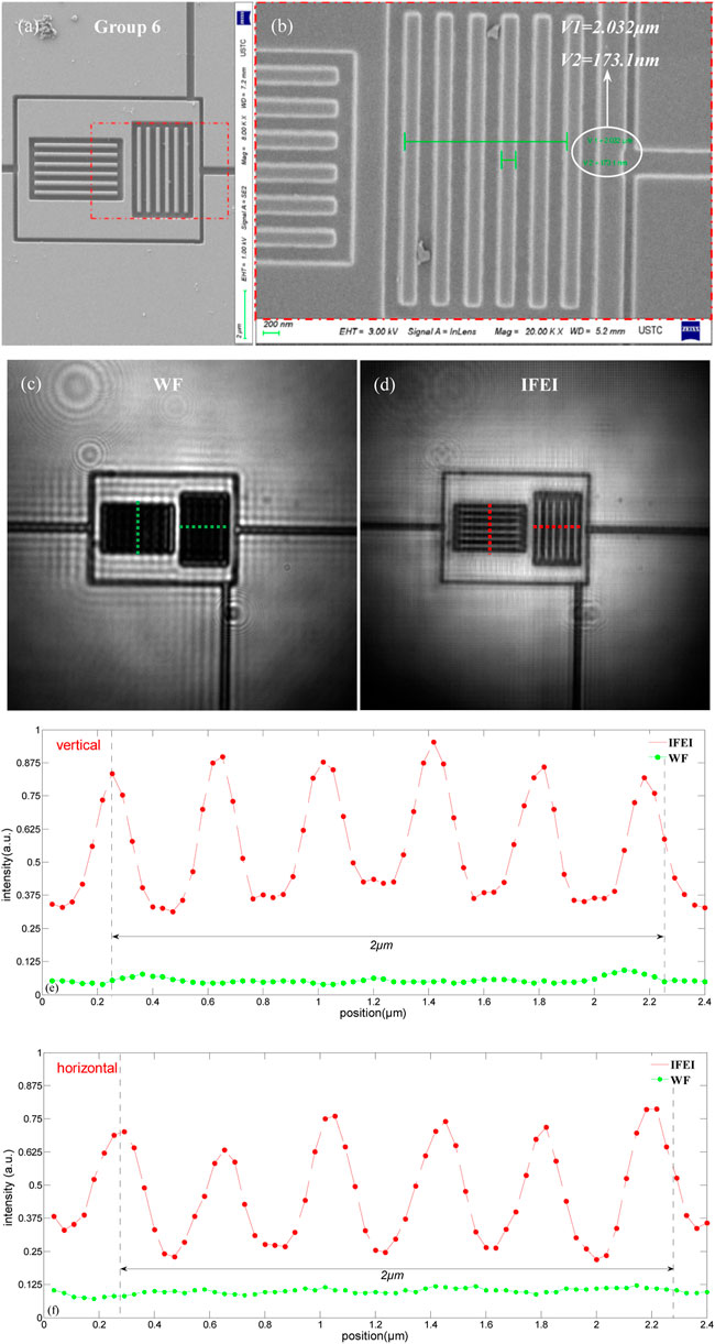
FIGURE 3. Results of the SEM imaging, conventional WF imaging and IFEI imaging for the COE. (A,B) show the SEM images of 0.2 μM scratches; (C,D) show the wide-field images and IFEI reconstruction images of 0.2 μM scratches, respectively; (E,F) are the vertical and horizontal cross-sectional intensity distributions of wide-field images and IFEI reconstructions imaging along the scratch line width of the images (C,D) (Red dashed lines is the IFEI and green is the wide-field).
Considering that the detection of dig defects is usually much more difficult than that of scratch defects, we subsequently carried out a high-resolution microscopic imaging experimental study on the dig defects on the surface of the COE with a diameter of ∼200 nm. Figures 4B,C are the wide-field imaging and high-resolution microscopic imaging of 200 nm digs based on IFEI. As shown in Figure 4D, the Gaussian fitting was performed on the light intensity distributions at the equator of the dig defects in Figure 4B,C. The full width at half maximum (FWHM) of the dig defect was ∼201.3 nm in the IFEI reconstruction image, which was close to the size calibrated by SEM in Figure 4, indicating that the IFEI system had high resolution detection ability for defects ≥200 nm on the surface of fused silica. In addition, the lateral size of the wide-field imaging of the dig defect shown in Figure 4D was ∼322.6 nm, which was bigger than the diffraction limit of the optics system. The reason might be due to the strong scattering effect based on the steep edge of the digs.
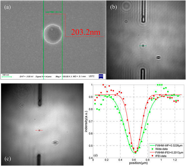
FIGURE 4. (A) SEM image of 0.2 μM dig defects on COE; (B) and (C) show the wide-field image and IFEI reconstruction image of 0.2 μM dig defects, respectively; (D) the intensity distribution of 0.2 μM dig along the dashed lines in (B,C) with the Gaussian fitting.
System resolution calibration
To further verify the lateral resolution of the home-built IFEI system, we selected gold nanoparticles with a diameter of ∼81 nm as the detection target. The size of the gold nanoparticles was far less than the theoretical diffraction limits of our imaging system. Figures 5B,C show the results of wide-field imaging and high-resolution microscopic imaging of 81 nm gold nanoparticles. Figure 5E,F depict the corresponding spectra of the nanoparticles obtained with Figures 5B,C, and the green dash circle represents the size of the CTF of the microscope system. From Figure 5E,F, it can be seen that the CTF had changed from the green dotted line area to the red dash line area, and the range of the CTF was enlarged in all directions. In other words, the isotropic improvement of the image resolution was achieved. After Gaussian fitting, the lateral resolution of the system under the wide-field imaging was ∼305.2 nm (green dotted line in Figure 5D), which was close to the theoretical optical diffraction limit of our optical system. Figure 5D shows the FWHMs of the nanoparticles at the dotted line in Figures 5B,C. As shown in Figure 5D, the lateral limit resolution of the high resolution imaging system was ∼179.5 nm, which was 1.72 times higher than the optical diffraction limit. In summary, we have achieved optical high-resolution microscopic imaging of the defects ≤200 nm on the surface of fused silica optics for the first time. Furthermore, it can be clearly seen from Figure 3D. Figure 4C that the IFEI system has a better imaging contrast for fused silica, compared with the Zhang et al [29] who have done similar research on the surface microstructure of resolution plates based on frequency-domain diagonal extension imaging, we not only have incomparable imaging contrast, but our system has a great advantage in resolution, which is less than one third of its limit resolution.
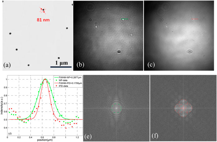
FIGURE 5. (A) SEM image of 81 nm gold nanoparticles; (B) and (C) show the wide-field image and IFEI reconstruction image of 81 nm gold nanoparticles, respectively; (D) the intensity distribution of nanoparticles along the dashed lines in (B,C) with the Gaussian fitting. (E,F) represent the spectra of the images (B,C).
Process certification
Finally, in order to evaluate the imaging effect of the self-developed IFEI high-resolution microscopic imaging system on the ultra-precision processed fused silica optics, Corning No.7980 fused silica specimen was selected as the test target (Figure 6A). Equal-spacing sampling measurement was used for evaluation. Firstly, a distinct defect was selected in the central area of the sample as the starting area, and then wide-field and IFEI scanning imaging were performed on the 4 × 3 sub-area of the specimen according to the scanning strategy in Figure 6B. The wide-field and high resolution imaging of each area are illustrated in Figures 7A,B respectively. Compared each of the area images in Figures 7A,B, it can be clearly seen that, the IFEI reconstruction imaging showed more details and higher contrast than wide-field imaging. For example, the scratch edge information in IFEI imaging had been greatly improved, which did not be distinguished in wide field imaging. The magnified and blurred digs in wide-field imaging were clearly distinguished by IFEI reconstruction images.
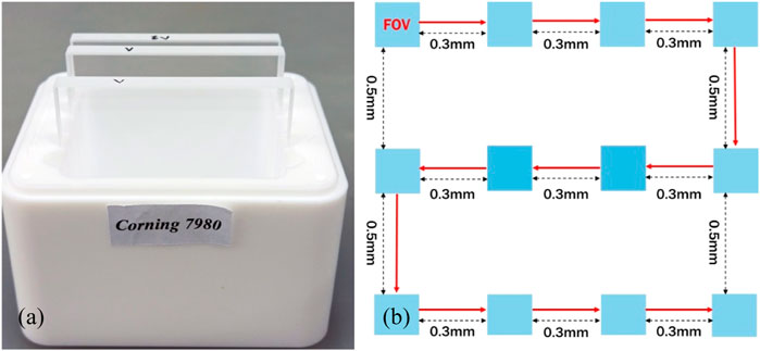
FIGURE 6. (A) Image of the ultra-precision processed fused silica sample. (B). Detection strategy.
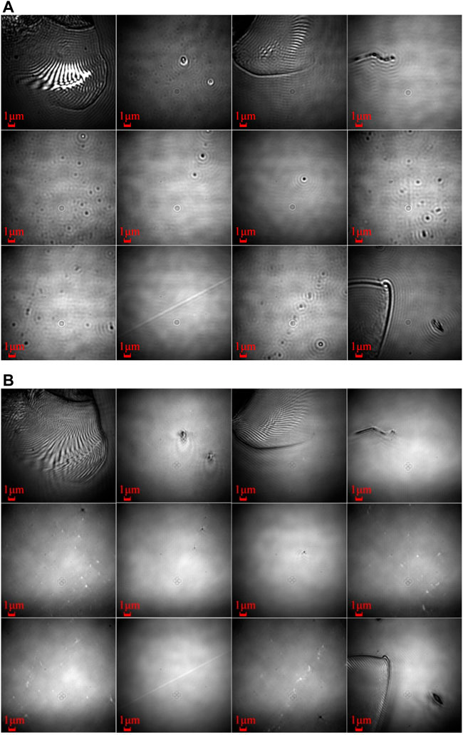
FIGURE 7. (A) The wide-field images and (B) the IFEI reconstruction images of 4 × 3 sub-area of the Corning No.7980 fused silica sample.
Methods for detecting surface defects of fused silica optics are summarized in Table 1. Compared with the dark field micro and conventional optical microscopy imaging, which are commonly used for surface defect detection of fused silica optics, the IFEI has excellent imaging resolution up to 179.5 nm. In addition, the IFEI not only has long work distance and high detection efficiency (field scanning), but also does not require special sample processing (SEM) and fluorescent labeling (STED, STORM, PALM). Using the IFEI, defect detection of fused silica optics with medium and large aperture will be realized by stitching scanning. And to highlight our work, some typical high resolution methods based on frequency-domain extension imaging are summarized in Table 2. It can be seen that our IFEI exhibits excellent performances especially in terms of resolution. Moreover, the detection efficiency is also competitive compared with other methods except for the FPM. But it must be noted that the detection speed of IFEI is mainly limited by the loading frequency of SLM, which can be improved by product upgraded and adopt other method to achieve phase grating switching. In future, we will further improve the imaging resolution of the detection system by adopting shorter-wavelength lasers, spatial frequency matching of structured light stripes, optimization of the system optical path and super-resolution reconstruction algorithm. It is expected to achieve defect detection of optical elements near 100 nm, which has an excellent application prospect in surface defect detection of high precision optical components and surface characteristics analysis of low-dimensional optical materials.
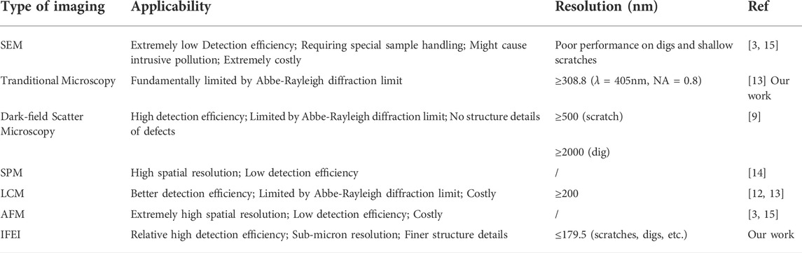
TABLE 1. Summaries of surface defect detection methods for fused silica optics.
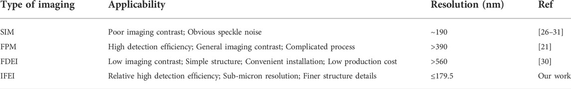
TABLE 2. Summaries of the detection of surface morphology of fused silica by frequency-domain extension imaging methods.
Conclusion
In summary, a high-resolution optical microscopy was used to detect ≤200 nm defects of fused silica optics based on IFEI for the first time, to the best of our knowledge. Based on a COE resolution plate, our self-developed high-resolution detection system effectively detected sub-micron scale calibration scratches, and residual random sub-micron defects might from industrial processing with a maximum imaging resolution up to ∼179.5 nm. Compared with the theoretical diffraction limit, the system resolution of IFEI imaging was increased by 1.72 times, which had a great significance to study the behavior and mechanism of high damage threshold defects-induced laser damages on fused silica optics.
Data availability statement
The original contributions presented in the study are included in the article/supplementary material, further inquiries can be directed to the corresponding author.
Author contributions
JB:Conceptualization, Validation, Writing Original Draft, Funding acquisition; LZ:Supervision, Writing Review.
Funding
This research is supported by the Youth Research Fund of Laser Fusion Research Center of China Academy of Engineering Physics.
Conflict of interest
The authors declare that the research was conducted in the absence of any commercial or financial relationships that could be construed as a potential conflict of interest.
Publisher’s note
All claims expressed in this article are solely those of the authors and do not necessarily represent those of their affiliated organizations, or those of the publisher, the editors and the reviewers. Any product that may be evaluated in this article, or claim that may be made by its manufacturer, is not guaranteed or endorsed by the publisher.
References
1. Liao ZM, Raymond B, Gaylord J, Fallejo R, Bude J, Wegner P. Damage modeling and statistical analysis of optics damage performance in MJ-class laser systems. Opt Express (2014) 23(22):28845–56. doi:10.1364/oe.22.028845
2. Liu TX, Yang K, Zhang Z, Yan LH, Huang BC, Li HY, et al. Hydrofluoric acid–based etching effect on surface pit, crack, and scratch and laser damage site of fused silica optics. Opt Express (2019) 27(8):10705–28. doi:10.1364/oe.27.010705
3. Shen N, Bude JD, Carr CW. Model laser damage precursors for high quality optical materials. Opt Express (2014) 22(3):3393–404. doi:10.1364/oe.22.003393
4. Carr CW, Radousky HB, Demos SG. Wavelength dependence of laser-induced damage: Determining the damage initiation mechanisms. Phys Rev Lett (2003) 91:127402. doi:10.1103/physrevlett.91.127402
5. Negres RA, Cross DA, Liao ZM, Matthews MJ, Carr CW. Growth model for laser-induced damage on the exit surface of fused silica under UV, ns laser irradiation. Opt Express (2014) 22(4):3824–44. doi:10.1364/oe.22.003824
6. Manes KR, Spaeth ML, Adams JJ, Bowers MW, Bude JD, Carr CW, et al. Damage mechanisms avoided or managed for NIF large optics. Fusion Sci Technol (2016) 69(1):146–249. doi:10.13182/fst15-139
7. Gao X, Feng GY, Han JH, Zhai LL. Investigation of laser-induced damage by various initiators on the subsurface of fused silica. Opt Express (2012) 20(20):22095–101. doi:10.1364/oe.20.022095
8. Laurence TA, Bude JD, Ly S, Shen N, Feit MD. Extracting the distribution of laser damage precursors on fused silica surfaces for 351 nm, 3 ns laser pulses at high fluences (20-150 J/cm2). Opt Express (2012) 20(10):11561–73. doi:10.1364/oe.20.011561
9. Li C, Yang YY, Chai HT, Zhang YH, Wu F, Zhou L, et al. Dark-field detection method of shallow scratches on the super-smooth optical surface based on the technology of adaptive smoothing and morphological differencing. Chin Opt Lett (2017) 15(8):081202. doi:10.3788/col201715.081202
10. Tao X, Xu D, Zhang ZT, Zhang F, Liu XL, Zhang DP. Weak scratch detection and defect classification methods for a large-aperture optical element. Opt Commun (2017) 387:390–400. doi:10.1016/j.optcom.2016.10.062
11. Huang J, Wang FR, Liu HJ, Geng F, Jiang XD, Sun LX, et al. Non-destructive evaluation of UV pulse laser-induced damage performance of fused silica optics. Sci Rep (2017) 1(1):16239–12. doi:10.1038/s41598-017-16467-2
12. Neauport J, Cormont P, Legros P, Ambard C, Destribats J. Imaging subsurface damage of grinded fused silica optics by confocal fluorescence microscopy. Opt Express (2009) 17(5):3543–54. doi:10.1364/oe.17.003543
13. Liu HJ, Ye X, Zhou XD, Huang J, Wang FR, Zhou XY, et al. Subsurface defects characterization and laser damage performance of fused silica optics during HF-etched process. Opt Mater (2014) 36:855–60. doi:10.1016/j.optmat.2013.11.022
14. Zeng JW, Darvishzadeh-Varcheie M, Albooyeh M, Rajaei M, Kamandi M, Veysi M, et al. Exclusive magnetic excitation enabled by structured light illumination in a nanoscale mie resonator. ACS Nano (2018) 12(12):12159–68. doi:10.1021/acsnano.8b05778
15. Bude J, Miller P, Baxamusa S, Shen N, Laurence T, Steele W, et al. High fluence laser damage precursors and their mitigation in fused silica. Opt Express (2014) 22(5):5839–51. doi:10.1364/oe.22.005839
17. Abbe E. Beitrage zur theorie des Mikroskops under mikroskopischen Wahrnehmung. Archiv fur mikroskopische Anatomie (1873) 9(1):456–68.
18. Hell SW, Wichmann J. Breaking the diffraction resolution limit by stimulated emission: Stimulated emission depletion fluorescence microscopy. Opt Lett (1994) 19(11):780–2. doi:10.1364/ol.19.000780
19. Berning S, Willig KI, Steffens H, Dibaj P, Hell SW. Nanoscopy in a living mouse brain. Science (2012) 335(6068):551. doi:10.1126/science.1215369
20. Zheng GA, Horstmeyer R, Yang CH. Wide-field, high-resolution Fourier ptychographic microscopy. Nat Photon (2014) 7(9):739–45. doi:10.1038/nphoton.2013.187
21. Zuo C, Sun JS, Li JJ, d Asundi A, Chen C. Wide-field high-resolution 3D microscopy with Fourier ptychographic diffraction tomography. Opt Lasers Eng (2020) 128:106003. doi:10.1016/j.optlaseng.2020.106003
22. Heintzmann R, Cremer CG. Laterally modulated excitation microscopy: Improvement of resolution by using a diffraction grating. Proc SPIE (1999) 3568:185–96.
23. Gustafsson MGL. Surpassing the lateral resolution limit by a factor of two using structured illumination microscopy. SHORT COMMUNICATION. J Microsc (2000) 198(2):82–7. doi:10.1046/j.1365-2818.2000.00710.x
24. Rust MJ, Bates M, Zhuang XW. Sub-diffraction-limit imaging by stochastic optical reconstruction microscopy (STORM). Nat Methods (2006) 3(10):793–6. doi:10.1038/nmeth929
25. Betzig E, Patterson GH, Sougrat R, Lindwasser OW, Olenych S, Bonifacino JS, et al. Imaging intracellular fluorescent proteins at nanometer resolution. Science (2006) 313(5793):1642–5. doi:10.1126/science.1127344
26. Littleton B, Lai K, Longstaff D, Sarafis V, Munroe P, Heckenberg N, et al. Coherent super-resolution microscopy via laterally structured illumination. Micron (2007) 38(2):150–7. doi:10.1016/j.micron.2006.07.010
27. Hajek KM, Littleton B, Turk D, McIntyre TJ, Rubinsztein-Dunlop H. A method for achieving super-resolved widefield CARS microscopy. Opt Express (2010) 18(18):19263–72. doi:10.1364/oe.18.019263
28. Chowdhury S, Dhalla A, Izatt J. Structured oblique illumination microscopy for enhanced resolution imaging of non-fluorescent, coherently scattering samples. Biomed Opt Express (2012) 3(8):1841–54. doi:10.1364/boe.3.001841
29. Chen JL, Xu Y, Lv XH, Lai XM, Zeng SQ. Super-resolution differential interference contrast microscopy by structured illumination. Opt Express (2013) 21(1):112–21. doi:10.1364/oe.21.000112
30. Jiang S, Guan ML, Wu JM, Fang GC, Xu XZ, Jin DY, et al. Frequency-domain diagonal extension imaging. Adv Photon (2020) 2(3):1. doi:10.1117/1.ap.2.3.036005
31. Ganjkhani Y, Calabuig A, Pedrini G, Moradi A. Oblique illumination lateral shearing digital holographic microscopy. J Opt (2020) 22:095601. doi:10.1088/2040-8986/aba4c0
32. Demmerle J, Innocent C, North AJ, Ball G, Müller M, Miron E, et al. Strategic and practical guidelines for successful structured illumination microscopy. Nat Protoc (2017) 12(5):988–1010. doi:10.1038/nprot.2017.019
33. Lal A, Shan CY, Xi P. Structured illumination microscopy image reconstruction algorithm. IEEE J Sel Top Quan Electron (2016) 22(4):50–63. doi:10.1109/jstqe.2016.2521542
34. Shroff SA, Fienup JR, Williams DR. Phase-shift estimation in sinusoidally illuminated images for lateral superresolution. J Opt Soc Am A (2009) 26(2):413–24. doi:10.1364/josaa.26.000413
35. Shroff SA, Fienup JR, Williams DR. Lateral superresolution using a posteriori phase shift estimation for a moving object: Experimental results. J Opt Soc Am A (2010) 27(8):1770–82. doi:10.1364/josaa.27.001770
36. Wicker K. Non-iterative determination of pattern phase in structured illumination microscopy using auto-correlations in Fourier space. Opt Express (2013) 21(21):24692–701. doi:10.1364/oe.21.024692
37. Zhou X, Dan D, Jia Q., Baoli Y., Lei M.. Super-resolution reconstruction theory in structured illumination microscopy. Acta. Optica Sinica. (2017) 37(3):0318001. doi:10.3788/aos201737.0318001
Keywords: microscopy, submicron-scale structure, super-resolution, laser induced breakdown, nanostructures
Citation: Bai J, Ren H, Shi Z, Ma H, Liu L, Ma K, Chai L and Zhang L (2022) Isotropy frequency-domain extension imaging and its application in detection of nanostructures. Front. Phys. 10:993435. doi: 10.3389/fphy.2022.993435
Received: 13 July 2022; Accepted: 09 August 2022;
Published: 30 August 2022.
Edited by:
Yunzheng Wang, Singapore University of Technology and Design, SingaporeReviewed by:
Jinwei Zeng, Huazhong University of Science and Technology, ChinaQing Wu, Harbin University of Science and Technology, China
Liu Zhengkun, University of Science and Technology of China, China
Copyright © 2022 Bai, Ren, Shi, Ma, Liu, Ma, Chai and Zhang. This is an open-access article distributed under the terms of the Creative Commons Attribution License (CC BY). The use, distribution or reproduction in other forums is permitted, provided the original author(s) and the copyright owner(s) are credited and that the original publication in this journal is cited, in accordance with accepted academic practice. No use, distribution or reproduction is permitted which does not comply with these terms.
*Correspondence: Lin Zhang, Mjc3NzA4MzYzQHFxLmNvbQ==