 Marco Ferrero1*
 Roberta Arcidiacono1,2
 Nicolò Cartiglia1Leonardo Lanteri1,3Luca Menzio1,2
 Arianna Morozzi4
 Francesco Moscatelli4,5Roberto Mulargia3Federico Siviero1Robert White1
 Valentina Sola1,3
- 1Istituto Nazionale di Fisica Nucleare, Torino, Italy
- 2Dipartimento di Scienze del Farmaco, Università del Piemonte Orientale, Novara, Italy
- 3Dipartimento di Fisica, Università degli Studi di Torino, Torino, Italy
- 4Istituto Nazionale di Fisica Nucleare, Perugia, Italy
- 5CNR-Istituto Officina dei Materiali (IOM), Perugia, Italy
This paper investigates the single-event burnout (SEB) effect in thin irradiated positive-intrinsic-negative (PiN) diodes and low-gain avalanche diodes (LGAD). SEB is a destructive event triggered in silicon sensors by the passage of a high-momentum charged particle. This effect arises in planar sensors under specific conditions: a significant ionization event caused by the particle’s passage and a very high electric field in the entire bulk region. The investigation of SEB was performed in two beam test campaigns: one at Deutsches Elektronen-Synchrotron (DESY) with an electron beam of
1 Introduction
The low-gain avalanche diode (LGAD) technology Pellegrini et al. [1] enhances traditional silicon sensor designs by incorporating moderate internal gain
Investigations performed by the CMS, ATLAS, and RD50 collaborations Sola [5]; Beresford et al. [6] led to the conclusion that an SEB is triggered by the passage of a single particle when a high electric field is present in the whole volume of the sensor. The SEB mechanism hypothesis can be explained in four steps:
The large amount of energy released by an SEB discharge is enough to melt the silicon lattice. The typical SEB marks are star-shaped craters located on the surface of the sensors; see Figure 1. Often, associated with the crater, two perpendicular cracks are visible on the surface, most likely running along the silicon crystal axis.
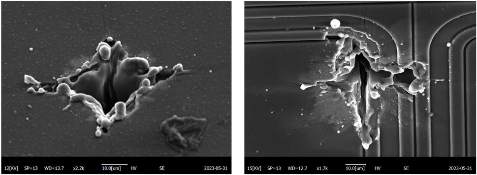
Figure 1. Scanning electron microscope (SEM) images of two typical SEB cross-shaped marks located in the middle of the pixel (left) and on the edge of the pixel (right). The sensors in the picture were produced by Hamamatsu Photonics (left) and Fondazione Bruno Kessler (right), with an active thickness of
The investigations performed on 55-µm- and
2 Materials and methods
2.1 Sensors under test
The sensors tested in the beam test campaigns were manufactured by Hamamatsu Photonics (HPK) and Fondazione Bruno Kessler (FBK). These sensors are part of the second HPK and the first FBK R
Figure 2 shows the key elements of an LGAD device. Each sensor has a pixel core and a pixel periphery. The pixel core is composed of a
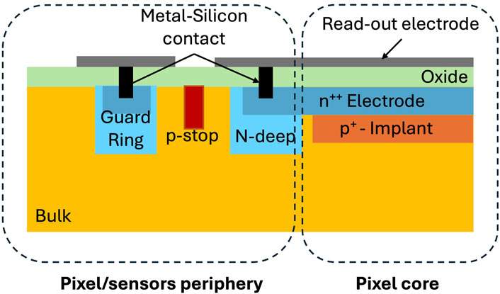
Figure 2. A typical cross section of an LGAD tested in the SEB campaigns. Left side: the sensor/pixel periphery composed of a guard ring and
The sensors investigated in this work are un-irradiated and irradiated LGADs and PiNs and span a sizeable interval in area, thickness, and number of pixels. The thickness ranges from
Figure 3. Types of sensor geometries tested during the beam test campaigns.

Table 1. Parameters of the tested sensors. The last column reports the values of the electric fields at which the sensors burned out
The irradiation of sensors was performed at the JSI TRIGA research reactor in Ljubljana Snoj et al. [11], with neutron fluences of 1 × 10¹⁵ neq/cm2, 2.5 × 10¹⁵ neq/cm2, 5 × 10¹⁵ neq/cm2, and 10
The sensors under test also include a set of non-irradiated PiNs that are able to reach
The wide range of geometries and irradiation levels of the sensors under test made it possible to study the relationship between the SEB and several parameters such as sensor active surface, capacitance, and active thickness.
2.2 CERN and DESY beam test facilities and beam characteristics
The SEB investigation is based on data collected in two beam test campaigns. The first campaign was performed at the DESY beam test facility situated in Hamburg–Bahrenfeld. This facility comprises three beam lines providing electrons or positrons with selectable momenta in the range
In DESY, the beam momentum was
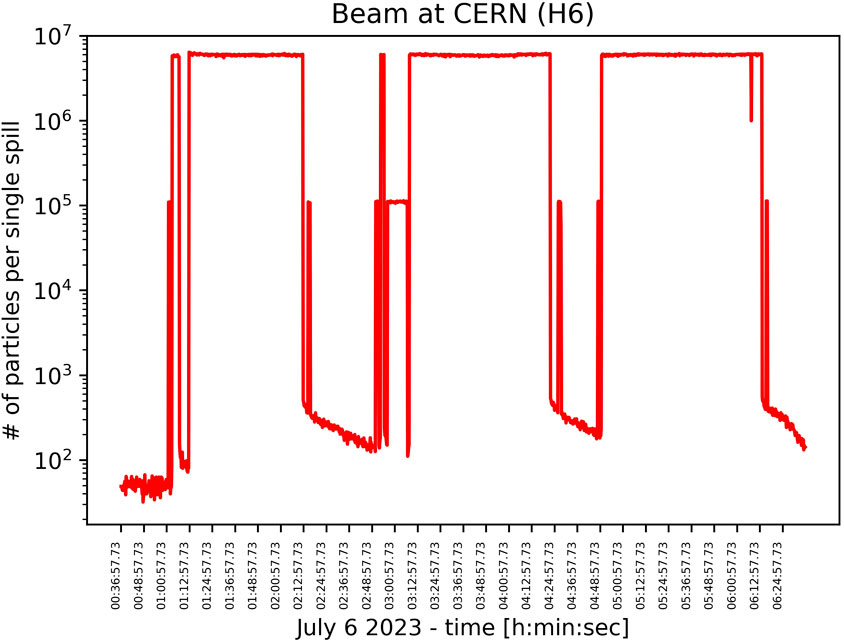
Figure 4. Number of particles per single beam spill monitored in a time window of 6 h during the beam test campaign at CERN. These data were extracted from CERN [13].
2.3 Experimental setup and sensors operations at beam tests
The sensors investigated in this work were mounted and bonded on read-out boards that provided the bias voltage to the backside of the sensor (the ohmic side) and kept all front electrodes and guard ring structures (the junction side) grounded.
To maximize the number of sensors tested simultaneously, a frame with several slots was designed and 3D printed. This frame accommodated up to six read-out boards, and it ensured a good alignment between the sensors and the beam. Figure 5 (top-left) reports a picture of the frame where the boards’ support fins are visible. The four central slots were used to house the sensors under test, while the two outermost slots housed sensors for monitoring the beam and the frame position.
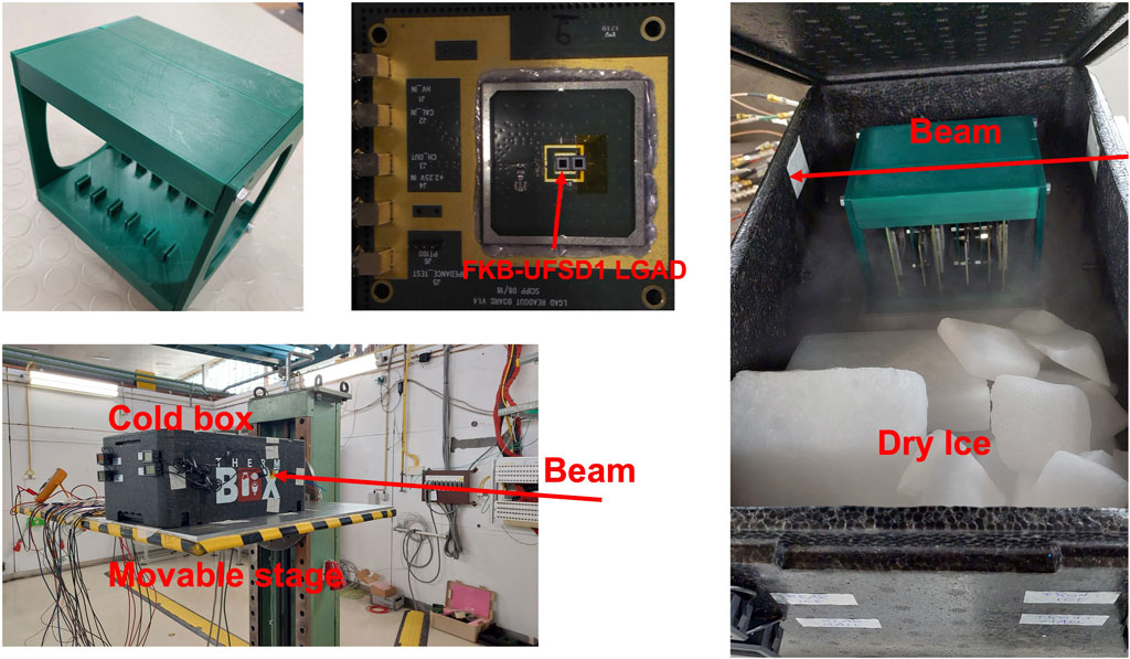
Figure 5. The experimental setup used at the DESY facility. Top left: Six-slot frame to support the read-out boards housing the DUTs. Top center: one of the two read-out boards with 300
The sensors used for beam monitoring, Figure 5 (top-center), are 300
The frame was positioned inside a hermetic polystyrene cold box. The box had a feed-through to provide the bias voltage to the sensors and to read out the monitoring devices. Solid carbon dioxide, also known as dry ice
The temperature inside the box volume was monitored during all beam campaigns using PT100 sensors mounted on the read-out boards near the DUTs. The temperature was very uniform along the beam direction, ensuring the same operation conditions for all sensors inside the frame; the sensors were operated in a temperature range between
3 Results
3.1 Measurement methodology
During the test, the electric field was gradually increased in steps of
The plots in Figure 6 (CERN beam campaign on the left, DESY on the right) report the fluence accumulated during the beam test for representative sensors as a function of the bulk electric field. The plots show that below
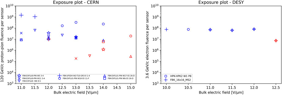
Figure 6. Fluence per sensor accumulated during the beam test as a function of the bulk electric field (left: CERN campaign; right: DESY campaign). Blue markers indicate the fluences and electric fields at which the sensors survived, and red markers correspond to conditions that led to burnout. Differences in fluence among the sensors are due to variations in active sensor surfaces and exposure times.
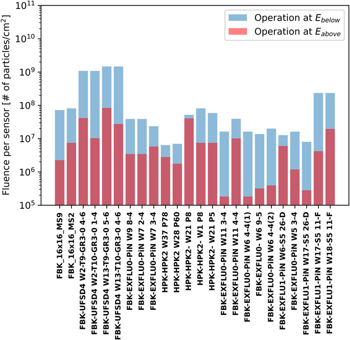
Figure 7. Fluence accumulated at the beam test at
One clear observation was that the probability of SEB occurrence did not increase with the increase in the active surface (which is linearly proportional to the capacitance) of devices exposed to the beam.
The fluences measured at CERN are underestimated by approximately
3.2 Parameters influencing the value of
The data reported in Figure 6 and Table 1 show the burnout field values
The average values of
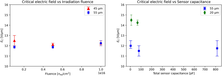
Figure 8. Left: average values of the critical electric field as a function of the irradiation fluence of EXFLU0 single-pad sensors with
Another factor that does not affect the SEB is the presence of the multiplication layer; both LGAD and PiN sensor types exhibited SEB at similar
A strong correlation between the sensor active thickness and
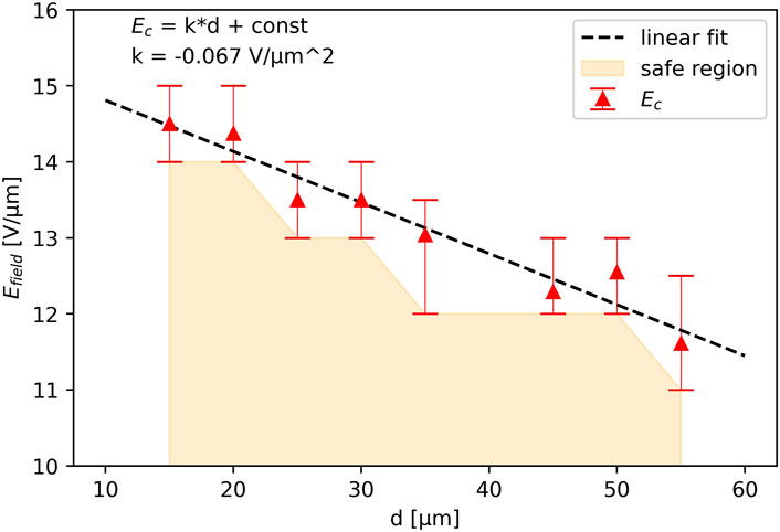
Figure 9. Relationship between the SEB electric field and the nominal active thickness of the sensors. The red markers correspond to the average
3.3 Optical inspection of burned-out sensors
Each burned-out sensor has been optically inspected under a microscope to locate the crater caused by the SEB. All broken sensors have a crater on the surface; in most cases, the craters have the typical cross-shape with evident breaks along the arms of the cross, as observed in previous studies: Sola [5]; Beresford et al. [6]; Laštovička-Medin et al. [7]. The craters are located in four sensor zones, as shown in Figure 10:
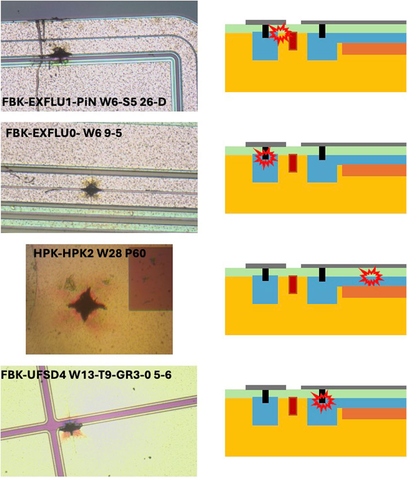
Figure 10. Left side: examples of craters visible in four different positions on the sensor surface. Right side: cross-section of LGADs with crater locations marked. From top to bottom, a crater on the i) guard ring edge, ii) guard ring metal contact, iii) pixel core, and iv) pixel metal contact.
Table 2 reports the statistics for each crater’s position listed above. In
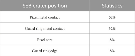
Table 2. Positions of the crater on the surface of the sensors.
There are several possible causes for the weakness of the pixel periphery:
1. The metal contact, locally, does not withstand the large amount of current flowing through it, causing the contact to melt.
2. The electric field in this region is higher due to the n-deep implant, which generates a deeper
3. The implants located in the pixel periphery generate a localized electric field higher than that in the bulk.
The listed hypotheses are not mutually exclusive; all of them could play a role in the SEB mechanism. Interestingly, one factor that appears to have no significant effect is the contact geometry: burnouts have been observed on both continuous and localized (circular) contacts, as shown in Figure 11, left and right, respectively.
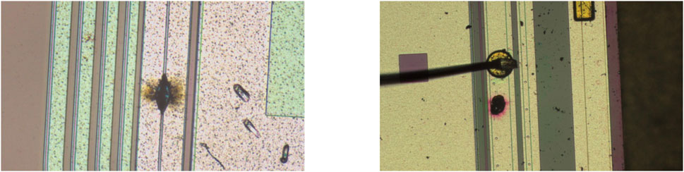
Figure 11. Left: crater located on a continuous contact. The line running vertically along the guard ring structure to the left of the pixel core represents the continuous metal contact; the crater (black spot) is located exactly on this line. Right: crater located on a localized circular contact. The small dots visible along the guard ring structure to the right of the pixel core correspond to circular metal contacts; in this case, the crater (the black spot with a red border) is located precisely on one of these contacts.
4 Conclusion
PiN diodes and LGADs, before and after irradiation, with a wide range of capacitance and active thickness
Data availability statement
The raw data supporting the conclusions of this article will be made available by the authors, without undue reservation.
Author contributions
MF: formal analysis, visualization, investigation, writing – original draft and writing – review and editing. RA: funding acquisition, investigation, writing – original draft and writing – review and editing. NC: resources, formal analysis, writing – original draft and writing – review and editing. LL: Investigation, writing – original draft and writing – review and editing. LM: Investigation, writing – original draft and writing – review and editing. AM: Investigation, writing – original draft and writing – review and editing. FM: writing – original draft and writing – review and editing. RM: Investigation, writing – original draft and writing – review and editing. FS: Investigation, writing – original draft and writing – review and editing. RW: Investigation, writing – original draft and writing – review and editing. VS: investigation, funding acquisition, formal analysis, writing – original draft and writing – review and editing.
Funding
The author(s) declare that financial support was received for the research and/or publication of this article. This project has received funding from the European Union’s Horizon Europe Research and Innovation Programme under Grant Agreements Nos 101004761 (AIDAinnova) and 101057511 (EURO-LABS). The work has been performed in collaboration with the INFN CSN5 “eXFlu” research project.
Acknowledgments
The measurements leading to these results have been performed at the Test Beam Facility at DESY Hamburg (Germany), a member of the Helmholtz Association (HGF), and at the SPS H6 Secondary Beam Line at CERN (Switzerland). The authors acknowledge CERN and DESY staff for their support during the beam test campaigns. They also acknowledge the Solid State research group of the Physics department of the University of Turin for the SEM pictures, particularly Pietro Aprà.
Conflict of interest
The authors declare that the research was conducted in the absence of any commercial or financial relationships that could be construed as a potential conflict of interest.
Generative AI statement
The author(s) declare that no Generative AI was used in the creation of this manuscript.
Publisher’s note
All claims expressed in this article are solely those of the authors and do not necessarily represent those of their affiliated organizations, or those of the publisher, the editors and the reviewers. Any product that may be evaluated in this article, or claim that may be made by its manufacturer, is not guaranteed or endorsed by the publisher.
Footnotes
1
2The probability is defined as 1/(particles required to induce an SEB).
References
1. Pellegrini G, Fernández-Martínez P, Baselga M, Fleta C, Flores D, Greco V, et al. Technology developments and first measurements of Low Gain Avalanche Detectors (LGAD) for high energy physics applications. Nucl Instr Methods Phys Res Section A: Acc Spectrometers, Detectors Associated Equipment (2014) 765:12–6. doi:10.1016/j.nima.2014.06.008
3. ATLAS. Technical design report: a high-granularity timing detector for the ATLAS phase-II upgrade. Tech Rep (2020).
4. Kramberger G, Baselga M, Cindro V, Fernandez-Martinez P, Flores D, Galloway Z, et al. Radiation effects in low gain avalanche detectors after hadron irradiations. J Instrumentation (2015) 10:P07006. doi:10.1088/1748-0221/10/07/P07006
5. Sola V. Systematic study of heavily irradiated LGAD stability using the Fermilab Test Beam Facility. In: Workshop on pico-second timing detectors for Physics (2021).
6. Beresford LA, Boumediene DE, Castillo-García L, Corpe LD, de Sousa MJD-C-S, El-Jarrari H, et al. Destructive breakdown studies of irradiated LGADs at beam tests for the ATLAS HGTD. J Instrumentation (2023) 18:P07030. doi:10.1088/1748-0221/18/07/P07030
7. Laštovička-Medin G, Rebarz M, Kramberger G, Laštovička T, Andreasson J, Precek M, et al. Studies of LGAD performance limitations, single event burnout and gain suppression, with femtosecond-laser and ion beams. Nucl Instr Methods Phys Res Section A: Acc Spectrometers, Detectors Associated Equipment (2022) 1041:167388. doi:10.1016/j.nima.2022.167388
8. Sola V, Morozzi A, Passeri D, Siviero F, Moscatelli F, Borghi G, et al. First results from thin silicon sensors irradiated to extreme fluence. In: PSD12: the 12th international conference on position sensitive detectors (2021).
9. Mulargia R, Arcidiacono R, Borghi G, Boscardin M, Cartiglia N, Vignalis MC, et al. Characterization of thin carbonated LGADs after irradiation up to 2.5 ⋅ 1015nMeveq/cm2. J Instrumentation (2024) 19:C04022. doi:10.1088/1748-0221/19/04/C04022
10. Paternoster G, Arcidiacono R, Boscardin M, Cartiglia N, Cenna F, Betta GD, et al. Developments and first measurements of ultra-fast silicon detectors produced at FBK. J Instrumentation (2017) 12:C02077. doi:10.1088/1748-0221/12/02/C02077
11. Snoj L, Žerovnik G, Trkov A. Computational analysis of irradiation facilities at the JSI TRIGA reactor. Appl Radiat Isot (2012) 70:483–8. doi:10.1016/j.apradiso.2011.11.042
12. Diener R, Dreyling-Eschweiler J, Ehrlichmann H, Gregor I, Kötz U, Krämer U, et al. The DESY II test beam facility. Nucl Instr Methods Phys Res Section A: Acc Spectrometers, Detectors Associated Equipment (2019) 922:265–86. doi:10.1016/j.nima.2018.11.133
13. CERN. Timber: CERN accelerator logging service (2023). Available online at: https://timber.cern.ch/. (accessed 1 July 2023 - 11 July 2023)
Keywords: single-event burnout, SEB, thin silicon sensors, PiN, LGAD
Citation: Ferrero M, Arcidiacono R, Cartiglia N, Lanteri L, Menzio L, Morozzi A, Moscatelli F, Mulargia R, Siviero F, White R and Sola V (2025) First study of single-event burnout in very-thin planar silicon sensors. Front. Phys. 13:1575672. doi: 10.3389/fphy.2025.1575672
Received: 12 February 2025; Accepted: 28 April 2025;
Published: 30 May 2025.
Edited by:
Francesco Barile, University of Bari Aldo Moro, ItalyReviewed by:
Bhartendu K. Singh, Banaras Hindu University, IndiaErika Catano-Mur, College of William & Mary, United States
Copyright © 2025 Ferrero, Arcidiacono, Cartiglia, Lanteri, Menzio, Morozzi, Moscatelli, Mulargia, Siviero, White and Sola. This is an open-access article distributed under the terms of the Creative Commons Attribution License (CC BY). The use, distribution or reproduction in other forums is permitted, provided the original author(s) and the copyright owner(s) are credited and that the original publication in this journal is cited, in accordance with accepted academic practice. No use, distribution or reproduction is permitted which does not comply with these terms.
*Correspondence: Marco Ferrero, bWFyY28uZmVycmVyb0B0by5pbmZuLml0