 Zhenghua Tang
 Dajun Lei
 Jianquan Huang
 Yaqi Chen
- Microelectronics and Optoelectronics Technology Key Laboratory of Hunan Higher Education, School of Physics and Electronic Electrical Engineering, Xiangnan University, Chenzhou, China
We propose a novel acoustic switch based on piezoelectric superlattices that is tunable by an external direct-current electric field. Our design harnesses the intrinsic coupling between acoustic waves and the oscillations of electric dipole moments within piezoelectric domains, which concurrently generate electromagnetic waves. The periodic modulation of the piezoelectric coefficient folds the phonon dispersion, leading to the intersection and hybridization with the electromagnetic dispersion branch and thereby opening a polaritonic band gap that governs acoustic wave propagation. Numerical simulations reveal that the absolute bandwidth of the first band gap near 10 GHz increases continuously from 0.003 GHz to 0.9 GHz as the electric field is raised from 0 V/m to 1.343 × 10⁶ V/m. Compared with previous acoustic switches, which rely on phase transformations, nonlinear deformations, or radiation pressure, the proposed device operates at much higher frequencies, features continuous and reversible tunability via the electro-optic effect, and benefits from a compact design. Moreover, the observed consistency between the band gaps for acoustic and electromagnetic waves confirms the dual control capability of the switch. These features make the proposed acoustic switch promising for high-frequency acoustic modulation and integrated microwave filtering applications.
1 Introduction
Acoustic switches, which selectively inhibit the propagation of acoustic waves within specific frequency ranges, have attracted considerable attention in communication and signal processing. Early implementations have relied on specially designed structures such as phononic metamaterials [1–4], topological Maxwell lattices [5, 6], phonon crystals [7–10], multi-layer 2D materials [11], phonon waveguides [12, 13], circular cavities [14], laser-controlled semiconductors [15], acoustic diodes [16–19], MEMS switches [20] and chemical switches [21]. In these systems, phonon band gaps typically emerge due to strong Bragg scattering at the boundaries of the Brillouin zone. However, most conventional approaches lack continuous and reversible tunability, a critical requirement for advanced dynamic modulation.
For example, the transmission of acoustic energy in an acoustic diode is regulated by radiation pressure effects [16]. A tunable phononic crystal plate with Y-shaped prisms is designed to support valley transport of elastic waves. Rotating the prisms breaks mirror symmetry and creates a new bandgap [22]. Similarly, studies on prestress effects in dispersion diagrams have demonstrated that the bandwidth of a specific band gap can be expanded or contracted via inertial amplification mechanisms [23]. In a planar resonator-based phononic metamaterial [1], tuning the uniform prestress transforms the phonon dispersion from a phonon-like to an optical-like character. Moreover, phase transitions within phononic crystals [8] affect both the location and width of the band gap, and nonreciprocal transmission in Maxwell lattices [5] can be switched by inducing topological phase transitions.
Other techniques further expand the range of tunable acoustic control strategies. For instance, local symmetry breaking in metamaterials can be exploited to create switchable topological phonon channels [24], while the geometric nonlinearity of an arch beam enables dynamic modulation of acoustic properties [12]. Additionally, the dynamical characteristics of graphene bilayers can be adjusted by varying the twist angle in magneto-mechanical multilayers [11], offering another avenue for acoustic manipulation. Recent studies have underscored the potential of piezoelectric materials for actively controlling acoustic propagation [25]. In particular, piezoelectric superlattices have been shown to generate polaritonic band gaps through the coupling of lattice vibrations and electromagnetic waves [26–28]. Prior studies on tunable devices primarily focused on optical or terahertz regimes. For instance [29], achieved high transmittance and Faraday rotation in magneto-photonic crystals, while [30] utilized graphene-polymer heterostructures for multi-channel filtering. In contrast, our work pioneers the integration of piezoelectric and electro-optic effects for GHz acoustic switching.
In this work, we design an acoustic switch based on piezoelectric superlattices wherein an applied DC electric field modulates the band structure. The key mechanism is that the inherent inversion symmetry breaking in piezoelectric materials generates electric dipole moments. When an acoustic wave impinges perpendicularly on the surface of the superlattice, it induces relative oscillations in these dipole moments. These oscillations give rise to alternating electromagnetic fields and, consequently, electromagnetic waves. Concurrently, the periodic modulation of the piezoelectric coefficient folds the phonon dispersion branch; the subsequent intersection and hybridization with the photon dispersion branch open up a band gap that forms the basis for acoustic switching. This dual-control mechanism, which has been hinted at in recent studies [31], forms the operational foundation of our device.
The acoustic switch is realized by employing piezoelectric superlattices with electrical polarization along the z-axis and an externally applied electric field in the same direction, as illustrated in Figure 1. Three key aspects of the acoustic switch are emphasized: (1) When an acoustic wave interacts with the structure, it excites electromagnetic waves due to dipole moment oscillations. (2) The resulting band gaps regulate the propagation of both acoustic and electromagnetic waves simultaneously. (3) The band gap width can be continuously and reversibly adjusted by varying the applied electric field via the electro-optic effect.
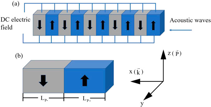
Figure 1. Schematic diagram of the acoustic switch based on piezoelectric superlattices with an external DC electric field along the z-axis. (a) Overall schematic of the acoustic switch and (b) illustration of the unit cell of the structure. The piezoelectric domains polarized along the
The remainder of this paper is organized as follows. In Section 2, we describe the theoretical configuration of the acoustic switch and presents the fundamental dynamic equations that govern its behavior. In Section 3, we present a numerical analysis of the transmission spectra for both acoustic and electromagnetic waves under various external electric fields, computed via the transfer matrix method, and provide a detailed discussion of the results. Finally, Section 4 concludes the paper with a summary of our findings and an outlook on potential future research directions.
2 The theoretical configuration and dynamical equations
As shown in Figure 1, the proposed acoustic switch is constructed using a one-dimensional array of piezoelectric superlattice units. Each unit cell consists of two piezoelectric domains with opposite polarizations along the z-axis. The domain thickness
When an acoustic wave impinges on the piezoelectric superlattice, it exerts mechanical stress on the piezoelectric domains. Due to the lack of inversion symmetry, this stress alters the local electric dipole moments, which in turn generates an alternating electromagnetic field that couples back to the mechanical lattice vibrations.
In this configuration, the longitudinal lattice displacement
Here,
The formation of the tunable band gap in our acoustic switch is based on three fundamental steps: (1) When an acoustic wave is incident on the structure, it exerts stress on the piezoelectric domains, causing them to vibrate and deform. Since piezoelectric materials lack inversion symmetry, the misalignment of positive and negative charge centers leads to the formation of electric dipole moments. The deformation changes both the magnitude and direction of these dipole moments, thereby exciting an alternating electromagnetic field. This deformation excites an alternating electromagnetic field, a phenomenon well documented in recent experimental studies [36]. (2) The periodic modulation of the piezoelectric coefficient in the superlattice leads to a folding of the phonon dispersion curve, effectively bringing the phonon and photon dispersion branches into proximity [26]. (3) The folded phonon branch intersects and hybridizes with the electromagnetic dispersion branch, opening a band gap that controls the propagation of both elastic and electromagnetic waves.
Consequently, the dynamic properties of the structure can be fully described by the coupled Maxwell’s equations and lattice vibration equations. By solving Equations 1–3 in a uniform piezoelectric domain, two pairs of eigensolutions are obtained—one pair representing the acoustic mode and the other pair representing the electromagnetic mode. A general solution can be formed as a linear combination of these eigensolutions. Using the continuity conditions for the transverse electric field, magnetic field, stress, and lattice displacement at the interfaces between piezoelectric domains, the fundamental properties of the piezoelectric domains can be encapsulated in a matrix
For the theoretical configuration shown in Figure 1, when acoustic waves are incident on the structure, both acoustic waves and electromagnetic waves are emitted from the opposite end. The transmitted amplitudes of acoustic and electromagnetic waves are represented by
and the parameters
3 Numerical results and discussion
In this work, the ferroelectric compound PZT is selected as the candidate material for constructing the acoustic switch because its complete material parameters are available and it exhibits a significant electro-optic effect. By substituting the material parameters of PZT into Equations 1–3 [32], the dimensionless coefficients are computed as
With reference to Equations 5–9, the superlattice transmission coefficients are obtained by successively multiplying the transmission matrices of each homogeneous layer, while enforcing stress continuity at the interfaces between the layers and the surrounding air. Figure 2 illustrates these transmission coefficients as a function of frequency for different numbers of periods.
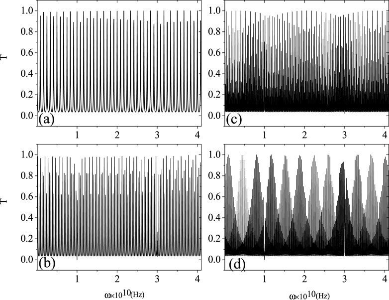
Figure 2. Transmission coefficients of acoustic waves for different numbers of periods: (a) four periods, (b) 16 periods, (c) 256 periods, (d) 16,384 periods, corresponding to the acoustic switch configuration shown in Figure 1 at
In a piezoelectric superlattice, the coupling between the mechanical vibrations (phonons) and the electromagnetic waves (photons) gives rise to polaritons. With only a few periods, the interaction between these modes is present but not fully developed. As a result, the transmission spectrum shows broader resonances with less pronounced polaritonic features. The limited number of interfaces offers only a weak opportunity for the phonon and photon branches to interact, so the hybridization that leads to the formation of a polariton band gap is not yet fully established.
As the number of periods increases, the repeated structure significantly enhances the coupling between the phononic and photonic modes. This stronger interaction results in more robust hybridization and the emergence of a well-defined polariton band gap. In this regime, the energy separation between the hybridized modes becomes more distinct, and the band gap edges sharpen due to the cumulative effect of many periodic interfaces. This leads to a significant suppression of transmission within the gap, as the mixed modes no longer propagate efficiently.
Outside the polariton band gap, the transmission spectra display passbands where energy is transmitted. With more periods, these passbands evolve to exhibit narrower resonance peaks. This indicates the presence of high-quality polariton modes, in which energy is confined and the group velocity is significantly reduced near the band edges. The increasing number of periods enhances mode selectivity. Only specific polaritonic states can constructively interfere and propagate, resulting in sharply defined transmission peaks.
Figures 2A–C clearly show that no stable band gap is present, primarily because the limited number of periods does not allow for sufficient cumulative coupling between the phonon and photon modes to establish a well-defined polariton band gap. However, Figure 2D reveals a band gap at
To expand the operational range of the acoustic switch, it is essential to develop a method for adjusting the band gap width. Applying an electric field along the z-axis to the piezoelectric superlattice enables the band gap to be tuned freely. The underlying mechanism is as follows: an applied electric field alters the dielectric constant of the piezoelectric domains via the electro-optic effect. This change, in turn, modifies the electromechanical coefficient, leading to variations in the band gap. Consequently, an external electric field can transition the device between passband and forbidden band states. Transmission coefficients for a structure with 65,536 periods are calculated and presented in Figures 3A–E.
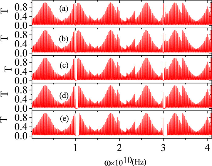
Figure 3. Transmission spectra of acoustic waves at various DC electric fields for an acoustic switch comprising 65,536 periods: (a) 0 V/m, (b)
As the external DC field increases (from 0 V/m to
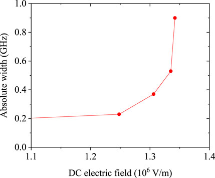
Figure 4. The evolution of the absolute bandwidth under an applied DC electric field is investigated using domain thicknesses identical to those shown in Figure 1, and with the number of periods in the entire structure matching that in Figure 3.
Considering practical implementation, based on our numerical simulations, the tunable band gap near 10 GHz is achieved by applying a DC electric field from 0 V/m up to
To illustrate the relationship between the band gap and the applied electric field more clearly, the transmission spectra for acoustic waves around 30 GHz are enlarged and replotted in Figure 5. Figure 5A shows that, in the absence of an external electric field, the band gap is very narrow. As the field increases, the left band edge remains nearly fixed while the right band edge shifts from 30.002 GHz to 30.86 GHz, causing the absolute bandwidth to expand from 0.002 GHz to 0.86 GHz. This result confirms that the forbidden band controlling the phonon flow can be tuned freely via the electro-optic effect, rendering the acoustic switch highly adaptable.
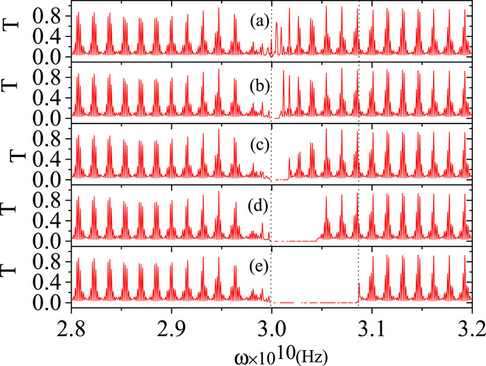
Figure 5. Transmission spectra of acoustic waves in the frequency range ω = 2.8–3.2 GHz for different DC electric field, for an acoustic switch with 65,536 periods: (a) 0 V/m, (b)
When acoustic waves impinge on the piezoelectric superlattice, both acoustic and electromagnetic waves are generated. By combining the transfer matrix from Equation 4 with the transmission coefficient for electromagnetic waves from Equation 6, the transmission coefficient for electromagnetic waves under acoustic excitation is calculated and shown in Figure 6. For a superlattice comprising 16 periods, Figure 6A reveals two dominant transmission peaks around 30 GHz without any stable photon band gap. As the total number of periods increases from 16 to 16,384, the number of electromagnetic transmission peaks increases, although the magnitude of the emitted electromagnetic waves remains relatively small.
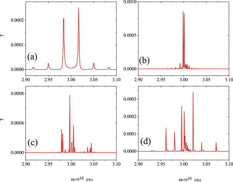
Figure 6. Transmission coefficients for electromagnetic waves in the frequency range ω = 2.90–3.10 GHz, corresponding to: (a) 16 periods, (b) 256 periods, (c) 4,096 periods, and (d) 16,384 periods. The domain thicknesses are identical to those in Figure 1.
The generation of electromagnetic waves can be explained by a two-step process. First, the inherent inversion symmetry breaking in the piezoelectric domains leads to the formation of electric dipole moments. Second, the longitudinal vibration of the acoustic waves induces stress at the interfaces between the domains, deforming them and thereby altering the magnitude and direction of the electric dipole moments. This process results in the emission of electromagnetic waves from the superlattice, as confirmed by the transmission spectra in Figure 6.
Figure 6 presents the electromagnetic transmission spectra in the absence of an applied electric field. To further assess the impact of an external electric field on electromagnetic transmission, Figure 7 shows the corresponding spectra under field application. A clear transmission peak and a stable band gap are observed around 30 GHz. Notably, while the left edge of the band gap remains essentially fixed at 30 GHz, the right edge shifts from 30.002 GHz to 30.86 GHz with increasing electric field. The consistency between the band gaps for acoustic waves (Figure 5) and electromagnetic waves (Figure 7) demonstrates that the band gap simultaneously controls both phonon and photon propagation. Essentially, this is a polariton band gap that manipulates the flow of both acoustic and electromagnetic waves.
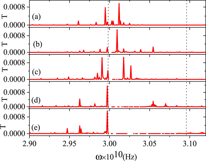
Figure 7. Transmission coefficients of electromagnetic waves in the frequency range ω = 2.90–3.12 GHz under various DC electric fields for an acoustic switch with 65,536 periods: (a) 0 V/m, (b)
Operating bandwidth and tunability are the key parameters defining the performance of the acoustic switch. The maximum operating frequency is determined by the thickness of the ferroelectric domains; increasing the thickness of one period in the superlattice enables the switch to operate at lower frequencies, albeit with a corresponding change in the operating bandwidth. Thus, altering the unit cell size provides an additional means of tuning the frequency band of the acoustic switch.
While adjusting the thickness of the piezoelectric superlattice after fabrication is challenging, the band gap of the acoustic switch can be effectively tuned via the applied electric field through the electro-optic effect. This field-induced tuning stems from the coupling between electromagnetic and acoustic waves, ensuring stable performance. For instance, the width of the first forbidden band can be varied from 0.003 GHz to 0.9 GHz as the external electric field increases from 0 V/m to
This approach is in stark contrast to previous methods of tuning acoustic switches, such as those based on phase transformations in phononic crystals, nonlinear deformation of arch beams, or the radiation pressure effect. In phononic crystals, the forbidden band can be adjusted by about 700 Hz through nonlinear deformation of an arch beam [12] or by an order of magnitude of 104 Hz in a one-dimensional structure with a 40-mm size. In comparison, the piezoelectric superlattice acoustic switch not only operates at higher frequencies but also exhibits a significantly wider operating bandwidth and enhanced tunability via external DC electric fields.
Earlier approaches to acoustic switching have typically operated at frequencies on the order of tens of kilohertz [16, 20, 21]. In our design, modulation is achieved at GHz frequencies, providing a substantial enhancement in performance. Moreover, the continuous and reversible tuning of the band gap via an external DC electric field offers dynamic control without necessitating permanent structural modifications. Recent advances in microfabrication and domain engineering [39] further underscore the scalability and practical applicability of our acoustic switch.
The unique features of the acoustic switch, such as its operation at GHz frequencies, continuous tunability via an external DC electric field, and the dual control of both acoustic and electromagnetic waves, open up several promising real-world applications. For instance, the switch could be integrated into microwave filtering circuits where dynamic reconfigurability is essential for managing signal interference [35]. Additionally, the compact and tunable design is also ideal for integration into MEMS-based sensors and actuators, enabling adaptive sensing technologies [20]. Furthermore, the dual acoustic-photonic control mechanism presents opportunities for hybrid systems, such as acousto-optic modulators or even acoustic logic circuits for novel low-power computing architectures [40].
While the current design uses PZT for its strong electro-optic effect and well-established properties, other piezoelectric materials such as BaTiO3 and PMN-PT may serve as alternatives depending on specific application needs, due to their distinct electromechanical characteristics [41]. Additionally, composite structures such as multilayer heterostructures and nanocomposites can be engineered to optimize phonon dispersion, reduce losses, and enhance control over acoustic wave propagation [42]. The integration of 2D materials like graphene or MoS2 offers further potential for improving energy efficiency and expanding device functionality [11]. These alternatives may support broader tunability, improved compatibility with MEMS platforms, and new avenues for high-performance acoustic-photonics integration.
4 Summary and outlook
In summary, we have theoretically designed and modeled an acoustic switch based on piezoelectric superlattices, which can be tuned by an external DC electric field. The transmission spectra reveal that the device can effectively block the propagation of acoustic waves within a tunable frequency range while simultaneously modulating the generation of electromagnetic waves. The underlying mechanism, arising from the hybridization of the folded phonon and electromagnetic dispersion branches, enables a higher operating frequency and broader bandwidth compared with traditional acoustic switches. Moreover, the continuous and reversible tunability, combined with the compact design of the superlattice, renders this device promising for high-frequency acoustic modulation and integrated microwave filtering applications.
Future work will focus on experimental validation of the theoretical model, optimization of device parameters for enhanced performance, and exploration of potential applications in integrated photonic–acoustic systems [40]. Despite the promising features of the proposed acoustic switch, several practical challenges must be addressed for real-world implementation. One major concern is energy dissipation, which may arise from acoustic attenuation, dielectric losses, or imperfect coupling between acoustic and electromagnetic modes, potentially reducing the modulation efficiency. In addition, the fabrication complexity of piezoelectric superlattices with a large number of precisely defined domains poses significant technical challenges, especially in achieving uniform domain thickness, alignment, and interface quality. Moreover, further studies on the impact of domain engineering and fabrication tolerances will be crucial for practical implementations.
Several potential fabrication techniques could be considered for constructing the proposed piezoelectric superlattices. For example, thigh-quality ferroelectric PZT thin films can be deposited by RF magnetron sputtering, chemical vapor deposition (CVD), or pulsed-laser deposition (PLD) [43]. Subsequent electric-field poling or patterned-electrode schemes enable controlled domain inversion and polarization tuning [44]. Additionally, advanced lithography techniques (e.g., electron-beam lithography or photolithography) may be utilized to define the periodic structure with high precision [43]. These methods, combined with established microfabrication processes, provide a promising pathway toward realizing the intricate superlattice structures necessary for the acoustic switch.
Data availability statement
The raw data supporting the conclusions of this article will be made available by the authors, without undue reservation.
Author contributions
ZT: Writing – original draft. DL: Writing – review and editing, Conceptualization, Supervision. JH: Conceptualization, Writing – review and editing, Supervision. YC: Writing – original draft, Investigation.
Funding
The author(s) declare that financial support was received for the research and/or publication of this article. This work was supported by Chenzhou City Science and Technology Project [2021JCYJ05] and by Hunan Provincial Education Office [19A459]. This work was also supported by the Hunan Provincial–Municipal Joint Natural Science Project [2023JJ50390].
Conflict of interest
The authors declare that the research was conducted in the absence of any commercial or financial relationships that could be construed as a potential conflict of interest.
Generative AI statement
The author(s) declare that no Generative AI was used in the creation of this manuscript.
Publisher’s note
All claims expressed in this article are solely those of the authors and do not necessarily represent those of their affiliated organizations, or those of the publisher, the editors and the reviewers. Any product that may be evaluated in this article, or claim that may be made by its manufacturer, is not guaranteed or endorsed by the publisher.
References
1. Karki P, Paulose J. Stopping and reversing sound via dynamic dispersion tuning in a phononic metamaterial. Phys Rev Appl (2021) 15:034083. doi:10.1103/PhysRevApplied.15.034083
2. Jin Y, He L, Wen Z, Mortazavi B, Guo H, Torrent D, et al. Intelligent on-demand design of phononic metamaterials. Nanophotonics (2022) 11:439–60. doi:10.1515/nanoph-2021-0639
3. Mousavi SH, Khanikaev AB, Wang Z. Topologically protected elastic waves in phononic metamaterials. Nat commun (2015) 6: 8682. doi:10.1038/ncomms9682
4. Zhu W, Deng W, Liu Y, Lu J, Wang HX, Lin ZK, et al. Topological phononic metamaterials. Rep Prog Phys (2023) 86:106501. doi:10.1088/1361-6633/aceeee
5. Zhou D, Ma JH, Sun K, Gonella S, Mao XM. Switchable phonon diodes using nonlinear topological Maxwell lattices. Phys Rev B (2020) 101:104106. doi:10.1103//PhysRevB.101.104106
6. Rocklin DZ, Chen BG, Falk M, Vitelli V, Lubensky T. Mechanical Weyl modes in topological Maxwell lattices. Phys Rev Lett (2016) 116:135503. doi:10.1103/PhysRevLett.116.135503
7. Alaie S, Goettler DF, Su M, Leseman ZC, Reinke CM, El-Kady I. Thermal transport in phononic crystals and the observation of coherent phonon scattering at room temperature. Nat commun (2015) 6:7228. doi:10.1038/ncomms8228
8. Bian ZG, Zhou XL. Study on phononic crystals with finite-state band gaps. Mech. Adv Mater Struc (2019) 28:1322–7. doi:10.1080/15376494.2019.1666325
9. Li F, Chong C, Yang J, Kevrekidis PG, Daraio C. Wave transmission in time- and space-variant helicoidal phononic crystals. Phys Rev E (2014) 90:053201. doi:10.1103/PhysRevE.90.053201
10. Bahrami A, Alinejad-Naini M, Motaei F. A proposal for 1×4 phononic switch/demultiplexer using composite lattices. Solid State Commun (2021) 326:114179. doi:10.1016/j.ssc.2020.114179
11. Zhang K, Jiao WJ, Gonellay S. Tunable band gaps and symmetry breaking in magnetomechanical metastructures inspired by multilayer two-dimensional materials. Phys Rev B (2021) 104:L020301. doi:10.1103/PhysRevB.104.L020301
12. Nguyen BH, Zhuang X, Park HS, Rabczuk T. Topologically switchable behavior induced by an elastic instability in a phononic waveguide. J Appl Phys (2020) 127:245109. doi:10.1063/5.0005331
13. Hatanaka D, Dodel A, Mahboob I, Onomitsu K, Yamaguchi H. Phonon propagation dynamics in band-engineered one-dimensional phononic crystal waveguides. New J Phys (2015) 17:113032. doi:10.1088/1367-2630/17/11/113032
14. Sumikura H, Wang T, Li PN, Michel AU, Heler A, Jung LN, et al. Highly confined and switchable mid-Infrared surface phonon polariton resonances of planar circular cavities with a phase change material. Nano Lett (2019). 19:2549–54. doi:10.1021/acs.nanolett.9b00304
15. Mikhalevich VG, Streltsov VN. Laser-Controlled semiconductor acoustic switches and modulators. Phys Wave Phenom (2014) 22:284–6. doi:10.3103/S1541308X1404013X
16. Devaux T, Cebrecos A, Richoux O, Pagneux V, Tournat V. Acoustic radiation pressure for nonreciprocal transmission and switch effects. Nat Commun (2019) 10:3292. doi:10.1038/s41467-019-11305-7
17. Fu C, Wang B, Zhao T, Chen CQ. High efficiency and broadband acoustic diodes. Appl Phys Lett (2018) 112:051902. doi:10.1063/1.5020698
18. Liang B, Yuan B, Cheng J. Acoustic diode: rectification of acoustic energy flux in one-dimensional systems. Phys Rev Lett (2009) 103:104301. doi:10.1103/PhysRevLett.103.104301
19. Chen Y, Wu B, Su Y, Chen W. Tunable two-way unidirectional acoustic diodes: design and simulation. J Appl Mech (2019) 86:031010. doi:10.1115/1.4042321
20. Annamalai M, Palaniapan M, Wong WK. Acoustic phonon characterisation of fixed-fixed beam MEMS switch. Electron Lett (2009) (2009) 45:464–6. doi:10.1049/el.2009.3691
21. Wu YJ, Ou QD, Yin YF, Li Y, Ma WL, Yu WZ, et al. Chemical switching of low-loss phonon polaritons in α-MoO3 by hydrogen intercalation. Nat Commun (2020) 11:2646. doi:10.1038/s41467-020-16459-3
22. Gao N, Qu SC, Si L, Wang J, Chen WQ. Broadband topological valley transport of elastic wave in reconfigurable phononic crystal plate. Appl Phys Lett (2021) 118:063502. doi:10.1063/5.0036840
23. Miniaci M, Mazzotti M, Amendola A, Fraternali F. Effect of prestress on phononic band gaps induced by inertial amplication. Int J Sol Struct (2021) 216:156–66. doi:10.1016/j.ijsolstr.2020.12.011
24. Süsstrunk R, Zimmermann P, Huber SD. Switchable topological phonon channels. New J Phys (2017) 19:015013. doi:10.1088/1367-2630/aa591c
25. Ji G, Huber J. Recent progress in acoustic metamaterials and active piezoelectric acoustic metamaterials-a review. Appl Mater Today (2022) 26:101260. doi:10.1016/j.apmt.2021.101260
26. Zhu YY, Zhang XJ, Lu YQ, Chen YF, Zhu SN, Ming NB. New type of polariton in a piezoelectric superlattice. Phys Rev Lett (2003) 90:053903. doi:10.1103/PhysRevLett.90.053903
27. Zhang WY, Liu ZX, Wang ZL. Band structures and transmission spectra of piezoelectric superlattices. Phys Rev B (2005) 71:195114. doi:10.1103/PhysRevB.71.195114
28. Liu ZX, Zhang WY. Study of the phonon–polaritons in piezomagnetic superlattices using a generalized transfer matrix method. J Phys Condens Matter (2006) 18:9083–92. doi:10.1088/0953-8984/18/39/034
29. Ghasemi F, Razi S. Faraday rotator made of conjugated magneto active photonic crystal heterostructures. J Magn Magn Mater (2021) 538:168304. doi:10.1016/j.jmmm.2021.168304
30. Ghasemi F, Entezar SR, Razi S. Terahertz tunable photonic crystal optical filter containing graphene and nonlinear electro-optic polymer. Laser Phys (2019) 29:056201. doi:10.1088/1555-6611/ab05c2
31. Chen S, Fan Y, Fu Q, Wu H, Jin Y, Zheng J A review of tunable acoustic metamaterials. Appl Sci (2018) 8:1480. doi:10.3390/app8091480
32. Bichurin MI, Petrov VM, Srinivasan G. Theory of low-frequency magnetoelectric coupling in magnetostrictive-piezoelectric bilayers. Phys Rev B (2003) 68:054402. doi:10.1103/PhysRevB.68.054402
33. Kang TD, Xiao B, Avrutin V, Özgür Ü, Morkoc H, Park JW, et al. Large electro-optic effect in single-crystal Pb(Zr, Ti)O3(001) measured by spectroscopic ellipsometry. J Appl Phys (2008) 104:093103. doi:10.1063/1.3009655
34. George JP, Smet PF, Botterman J, Bliznuk V, Woestenborghs W, VanThourhout D, et al. Lanthanide-assisted deposition of strongly electro-optic PZT thin films on silicon: toward integrated active nanophotonic devices. ACS Appl Mater Inter (2015) 7:13350–9. doi:10.1021/acsami.5b01781
35. Tang ZH, Jiang ZS, Chen T, Lei DJ, Huang JQ, Qiu F, et al. Electro-optic tunable band-stop filters using piezoelectric superlattices. Phys Lett A (2018) 382:3090–4. doi:10.1016/j.physleta.2018.07.040
36. Luo B, Liang X, Chen H, Sun N, Lin H, Sun N. Gain enhancement and ground plane immunity of mechanically driven thin-film bulk acoustic resonator magnetoelectric antenna arrays. Adv Funct Mater (2024) 34:2403244. doi:10.1002/adfm.202403244
37. Meshkinzar A, Al-Jumaily AM. Cylindrical piezoelectric PZT transducers for sensing and actuation. Sensors (2023) 23(6):3042. doi:10.3390/s23063042
38. Zhu H, Huang Y, Guo W, Dong H, Xing Z, Mi Q. Study on the performance of lead zirconate titanate piezoelectric coating prepared by vacuum cold spraying. Green Manuf Open (2023) 1(3):N/A. doi:10.20517/gmo.2023.05
39. Yin C, Jiang X, Mann S, Tian L, Drinkwater BW. Acoustic trapping: an emerging tool for microfabrication technology. Small (2023) 19:2207917. doi:10.1002/smll.202207917
40. Tian H, Liu J, Dong B, Skehan JC, Zervas M, Kippenberg TJ, et al. Hybrid integrated photonics using bulk acoustic resonators. Nat commun (2020) 11:3073. doi:10.1038/s41467-020-16812-6
41. Shrout TR, Zhang SJ. Lead-free piezoelectric ceramics: alternatives for PZT? J Electroceram (2007) 19:113–26. doi:10.1007/s10832-007-9047-0
42. Ezzin H, Amor MB, Ghozlen MHB. Lamb waves propagation in layered piezoelectric/piezomagnetic plates. Ultrasonics (2017) 76:63–9. doi:10.1016/j.ultras.2016.12.016
43. Muralt P. Ferroelectric thin films for micro-sensors and actuators: areview. J Micromech Microeng (2000) 10(2):136. doi:10.1088/0960-1317/10/2/307
Keywords: piezoelectric superlattices, acoustic switch, electro-optic effect, tunability, transfer matrix method
Citation: Tang Z, Lei D, Huang J and Chen Y (2025) Electro-optically tunable acoustic switch based on piezoelectric superlattices. Front. Phys. 13:1593391. doi: 10.3389/fphy.2025.1593391
Received: 14 March 2025; Accepted: 05 May 2025;
Published: 26 May 2025.
Edited by:
Atsufumi Hirohata, Tohoku University, JapanReviewed by:
Francesco Scotognella, Polytechnic University of Turin, ItalySepehr Razi, Leibniz Institute of Photonic Technology (IPHT), Germany
Mai M. El-Masry, Thebes Academy, Egypt
Copyright © 2025 Tang, Lei, Huang and Chen. This is an open-access article distributed under the terms of the Creative Commons Attribution License (CC BY). The use, distribution or reproduction in other forums is permitted, provided the original author(s) and the copyright owner(s) are credited and that the original publication in this journal is cited, in accordance with accepted academic practice. No use, distribution or reproduction is permitted which does not comply with these terms.
*Correspondence: Zhenghua Tang, dGFuZ3poQHhudS5lZHUuY24=