 Kunito Fukuda1,2
 Naoki Asakawa1*
- 1Division of Molecular Science, Graduate School of Science and Technology, Gunma University, Kiryu, Japan
- 2Human Resources Cultivation Center, Gunma University, Kiryu, Japan
Spin-dependent space-charge-limited carrier conduction in a Schottky barrier diode using polycrystalline p-type π-conjugated molecular pentacene is explored using multiple-frequency electrically detected magnetic resonance (EDMR) spectroscopy with a variable-angle configuration. The measured EDMR spectra are decomposed into two components derived, respectively, from mobile and trapped positive polarons. The linewidth of the EDMR signal for the trapped polarons increases with increasing resonance magnetic field for an in-plane configuration where the normal vector of the device substrate is perpendicular to the resonance magnetic field, while it is independent of the field for an out-of-plane configuration. This difference is consistent with the pentacene arrangement on the device substrate, where pentacene molecules exhibit a uniaxial orientation on the out-of-substrate plane. By contrast, the mobile polarons do not show anisotropic behavior with respect to the resonance magnetic field, indicating that the anisotropic effect is averaged out owing to carrier motion. These results suggest that the orientational arrangements of polycrystalline pentacene molecules in a nano thin film play a crucial role in spin-dependent electrical conduction.
Introduction
Organic semiconductors exist in various polycrystalline forms, the morphologies of which affect the characteristics of electronic devices incorporating such semiconductors (Thorsmølle et al., 2009). In particular, for π-conjugated molecules, the device structure determines the optimal orientation of π-stacking planes, since carrier mobility varies depending on whether the direction of carrier transport is aligned with the direction of π-stacking (Lee et al., 2006). For example, for devices in which electrical current flows in-plane, such as typical field-effect transistors, an edge-on orientation of plate-like π-conjugated molecules on the substrate surface, with the direction of π-stacking parallel to the surface, is appropriate (Sakanoue and Sirringhaus, 2010). On the other hand, for structures such as typical solar cells and light-emitting devices, a face-on orientation of plate-like molecules, with the direction of π-stacking perpendicular to the substrate surface, is appropriate. Therefore, control of molecular orientation and arrangement on substrate surfaces is of particular importance in the fabrication of electronic devices.
Organic semiconductors have also attracted interest in the field of spintronics, because they have longer spin coherence times than inorganic semiconductors (Sanvito and Dediu, 2012), owing to their generally smaller hyperfine interactions (HFI) and spin–orbit coupling (SOC) (McCamey et al., 2008). However, despite their relative weakness, HFI and SOC play important roles in spin relaxation (Yu, 2012; Malissa et al., 2014) and in the spin Hall and inverse spin Hall effects (Ando et al., 2013; Sun et al., 2016). Furthermore, HFI and SOC have anisotropic Hamiltonians, and therefore, clarification of the effect of molecular arrangements upon spin carrier dynamics is important for realizing homogeneous device fabrication and improving performance.
Pentacene (the chemical structure of which is shown in Figure 2C) is a p-type organic semiconductor with high crystallinity and carrier mobility (~1 cm2 V−1 s−1). Because of these latter properties, thermally evaporated thin films of pentacene have been considered for use as active layers in organic field-effect transistors (OFETs), and in this context, the relationship between the morphology of these films and carrier mobility has been the subject of a number of studies (Yang et al., 2005; Gershenson et al., 2006; Honsho et al., 2013; Kim et al., 2014). Thin films produced by thermal evaporation contain both crystalline grains and disordered regions at the grain boundaries, with the degree of crystallinity being controllable by altering the evaporation conditions. The presence of disorder at the grain boundaries leads to a bottleneck for carrier conduction in these regions and is thus of particular importance with regard to device performance. Knowledge of the aggregation states of polycrystalline thin films is, therefore, indispensable for attempts to improve performance.
Additionally, optically detected magnetic resonance (ODMR) spectroscopy (Köhler et al., 1993) of pentacene has revealed a large difference in occupancy rate between excited triplet sublevels. This is the origin of the large spin polarization of pentacene, leading to its application as a spin polarization material for dynamic nuclear polarization (DNP) (Takeda et al., 2001; Tateishi et al., 2014). Furthermore, pentacene is of importance not only for electronics but also for spintronics, as exemplified by the generation of a pure spin current on a pentacene film (Tani et al., 2015) and by spin-dependent electrically conduction (Fukuda and Asakawa, 2017). It is known that spin relaxation in organic semiconductors depends on their carrier transport mechanisms. Carrier transport in pentacene is believed to be intermediate between band-like and hopping conduction (Sakai et al., 2016; Nakayama et al., 2017), varying depending on the morphology of the material. Therefore, determination of the relation between carrier transport and morphology is a central issue for spintronic applications of pentacene. Of course, the importance of morphology in organic spintronics is widely recognized. Nevertheless, the effects of molecular arrangements of π-conjugated molecules remain elusive.
Electrically detected magnetic resonance (EDMR) spectroscopy is a candidate for acquiring information about the relation between spin states of a carrier and carrier transport, because this method directly measures carrier conduction in a device. Separate information about HFI and SOC on a π-conjugated polymer can be obtained from multiple-frequency EDMR (mf-EDMR) measurements (Joshi et al., 2016). However, the limitations of the methodology used in previous work have precluded determination of the orientational distributions of HFI and SOC, and there have not been any reports of the orientational and resonance frequency dependences of HFI and SOC in organic semiconductors. Furthermore, in order to obtain more details of the influence of molecular arrangements, it would be desirable to use mf-EDMR to study the effects of the orientation of device elements with respect to an applied static magnetic field. However, the mf-EDMR instruments necessary for this task have not previously been available.
Various methods are available for multiple-frequency electron spin resonance (mf-ESR), using, for instance, a series of ESR instruments with a fixed microwave frequency (Krinichnvi et al., 2004) or stripline-type rather than resonator-type instruments at high frequency (>100 GHz) (Noe et al., 2013). Additionally, solenoid coils instead of a microwave cavity have been used in an mf-ESR apparatus at low frequencies of 1–60 MHz (Mizoguchi, 1995). For all of these mf-ESR instruments, however, various problems remain. First, since the measurement frequency is discrete and fixed, special equipment is required to vary the resonance frequency in a quasi-continuous manner. Second, they are not suitable for simultaneous ESR/EDMR measurements, the ESR part of which is needed for calibration of the external resonance magnetic field strength. With EDMR, it is difficult to make anisotropy measurements, even using mf-EDMR with a stripline (Baker et al., 2012) or a coplanar waveguide resonator (Joshi et al., 2016), and cylindrical cavity with a short plunger (Seck and Wyder, 1998), partly because the angle between the device element and the applied microwave direction has to be fixed.
In the previous paper published by us, we developed a custom-built mf-EDMR system with waveguide windows and simultaneous ESR/EDMR measurements were presented using the combined sample of P–N junction-type Silicon diode with DPPH powder (Fukuda and Asakawa, 2016). In another previous paper published by us, we focused on the relationship between EDMR line and J-V characteristics (Fukuda and Asakawa, 2017), but we did not perform mf-EDMR measurements on the pentacene device. In this article, we unravel the influence of molecular arrangements on the carrier spin state for space-charge-limited conduction in a pentacene Schottky barrier diode (PSBD), using the custom-built mf-EDMR system and a variable-angle mechanism for the device element. Here, we shall describe the very first example to implement multiple-frequency EDMR with a mechanism of angle-dependency. In details, we report on variation in the linewidth of EDMR peaks measured with two perpendicular orientations of the magnetic fields. The linewidth of the magnetic resonance for the Au/pentacene/Al device element with respect to external magnetic field is broader at θ = 0°, where θ is an angle between magnetic field vector and normal vector of the device substrate, than that at θ = 90°, which is due to a broadening of the Gaussian sub-peak, which is attributed to trapped polarons, compared to angular-independent Lorentzian component due to mobile polarons.
Materials and Methods
Figure 1A shows a schematic illustration of the fabricated PSBD with a three-layer structure in which the pentacene thin film is sandwiched by electrodes. Pentacene was purchased from Wako Pure Chemicals (Tokyo, Japan) and used as received. First, an Au bottom electrode was vapor-deposited using a custom-built resistive-heating thermal evaporator on a cleaned soda lime glass substrate (S1111, Matsunami Glass Ind. Ltd., Japan) under a pressure of 5 × 10⁻³ Pa achieved using a turbo molecular pump (YTP-50M, ULVAC, Kanagawa, Japan). Next, a pentacene thin film (of thickness 150–170 nm; see below) was deposited using another custom-built thermal evaporator at room temperature. Finally, an Al top electrode was deposited using yet another evaporator. The dimensions of the glass substrate were 20 mm × 20 mm, and this was cut into four pieces in order to mount it into the EDMR/ESR cavity(Figures 1B,C), with each device element having dimensions of 10 mm × 10 mm. The effective cross-sectional area of the single PSBD was 2 mm × 8 mm. Prior to Al deposition, an additional Au electrode was deposited under the Al electrode in order to reduce the contact resistance between the electrode and the external circuit by preventing the oxidized Al surface from making direct contact with the latter.
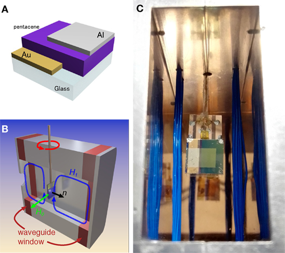
Figure 1. (A) Schematic structure of the pentacene Schottky barrier diode (PSBD). (B) Conceptual scheme of mf-EDMR. (C) PSBD mounted in the cavity.
In order to determine the electrical properties of the PSBD, current density versus voltage (J–V) curves were measured using a source-measurement meter (2612A, Keithley), with the Au and Al electrodes acting as anode and cathode, respectively (Figure 1A).
For the fabricated PSBD, out-of-plane grazing incidence wide-angle X-ray diffraction (GIWAXD) experiments were performed (Rint Ultima III, Rigaku, Tokyo, Japan), working at 40 kV and 40 mA, with Ni-filtered Cu Kα radiation (λ = 0.15418 nm) to confirm the crystalline structure and orientation of the pentacene molecule with respect to the substrate surface. 2θ scans were performed over an angular range of 3–25° at a rate of 0.08° min−1, with an angle of incidence α1 of 0.2°.
The thickness of the pentacene thin film in the PSBD was measured using tapping-mode atomic force microscopy (AFM; Nanopics 1000, Seiko Instruments, Inc.) of the film surface scratched by metal tweezers.
EDMR measurements were performed on the PSBD in two configurations determined by the angle θ between the external magnetic field vector H0 and the normal vector n to the substrate surface plane: parallel (θ = 0°) and perpendicular (θ = 90°). A custom-built mf-ESR/EDMR instrument based on the modified ESR/EDMR spectrometer reported in our previous work (Fukuda and Asakawa, 2016) was used. The resonance frequency was varied using a microwave cavity mounted with double waveguide windows of the same thickness, as shown in red in Figure 1B. The mf-EDMR measurements were performed by incorporating a multiple-frequency cavity in the EDMR system (Fukuda and Asakawa, 2016, 2017). Three independent measurements were repeated for three PSBDs, which were prepared using the same fabrication process, in order to clarify anisotropic behavior and magnetic field dependence. As shown in Figures 1B,C, the PSBD was mounted on a sample holder that could be rotated within the cavity (the sample holder can be seen above the PSBD in Figure 1C). The sample holder incorporated a wire supplying current to the PSBD and was equipped with four electrodes, the outer two of which provided the current path from the external constant-current circuit to the device, while the inner two were connected with ground to decrease noise. The multiple-frequency measurements were carried out at five microwave frequencies in the C-band. The voltage between two terminals of the PSBD under a forward constant-current density of J = 1.6 µA cm−2 was measured during a magnetic field sweep. The applied microwave irradiation of 3 W power was modulated with a rectangular amplitude of 800 Hz through a PIN diode switch, and the voltage variations induced by this irradiation were detected in a phase-sensitive manner by a lock-in technique. Furthermore, to improve the signal-to-noise ratio, the EDMR spectra were obtained by 100-times integration. The magnetic field was calibrated by magnetic field modulation ESR measurements of an N-doped Ib-type diamond (Sumicrystal CD2016(111)W, Sumitomo Electric Hardmetal, Japan). All measurements were performed at room temperature under ambient atmospheric conditions.
Results and Discussion
Figure 2A shows a typical J–V characteristic of the PSBD. This indicates the formation of a Schottky barrier at the pentacene/Al interface (Voz et al., 2005), thus confirming the successful fabrication of the device. The inset in Figure 2A shows a log–log plot of the J–V characteristic over the forward-bias range, with the horizontal dashed line corresponding to the current density of 1.6 µA cm−2 that was employed for the EDMR measurements. The forward current density lies in the so-called trap-free space-charge-limited conduction (SCLC) regime (Sze, 1981).
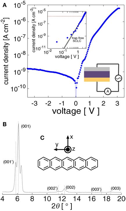
Figure 2. (A) Typical current density (J)–voltage (V) characteristic for the Au/pentacene/Al (PSBD) device at room temperature. The inset shows a double-logarithmic plot of the data from the PSBD with forward bias and the circuit for J-V measurements. The black dotted line represents the trap-free space-charge-limited conducting regime. The horizontal brown dashed line indicates the current density that was employed for the EDMR measurements. (B) Out-of-plane GIWAXD profile of the PSBD [reproduced from Fukuda and Asakawa (2017) with permission, copyright IOP Publishing]. (C) Chemical structure of pentacene.
We also performed out-of-plane GIWAXD measurements on the PSBD. Figure 2B shows a typical 2θ profile, which can be attributed to both the thin-film and bulk structures of the pentacene (Mattheus et al., 2003; Westermeier et al., 2014). The crystallographic axes of the pentacene molecule are shown in Figure 2C: the z-axis is parallel to the π-orbital and the y-axis is perpendicular to both the π-orbital and the C–H bonds. It is found that for pentacene in the thin films of the fabricated PSBDs, the y-axis is parallel to the normal vector of the substrate plane, while the x- and z-axes are randomly distributed in the plane, thus resulting in a uniaxial arrangement normal to the plane, which is derived from the fact that only (00n) and (00n´) peaks are visible in the X-ray diffraction chart.
Next, we carried out mf-EDMR measurements with θ = 0° and 90°. Figure 3 shows the EDMR spectra of PSBD. The linewidths at θ = 0° are broader than those at 90° for all experiments at the five microwave frequencies, indicating that the linewidth exhibits a clear anisotropy. Although the spectral change intuitively seems to be quite small, the difference of linewidth is an order of 1–10 Gauss, which corresponds to 3–30 MHz. Since ESR spectroscopy employs sinusoidal microwave of gigahertz range with precision of 1 Hz, we do not think the difference of 3–30 MHz as artifact. This anisotropy is consistent with previous observations at a microwave frequency of 5.5 GHz (Fukuda and Asakawa, 2017) (for the other spectra, see Figures S1–S3 in Supplementary Material). Anisotropic HFI with the protons in the pentacene molecule (Morton, 1964) and the molecular arrangement of the pentacene on the device substrate are responsible for the anisotropic linewidth of the EDMR spectra (Fukuda and Asakawa, 2017).
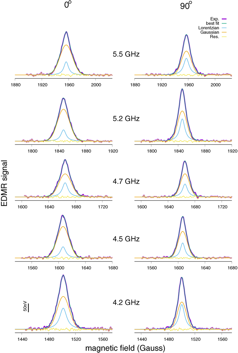
Figure 3. Multiple frequency EDMR spectra for PSBD. Microwave amplitude modulation (μAM)-EDMR spectra with a constant-current of about 1.6 µA cm−2 were obtained at a modulation frequency of 800 Hz. The EDMR spectra were obtained at a sweep rate of 20 G s−1 and with an averaging over 100 magnetic field sweeps under atmospheric pressure at room temperature. Typical EDMR spectra of PSBD at θ = 0° and 90° are shown, respectively. The results of fitting analyses for the EDMR spectra are also shown. The purple lines are the experimental results. The orange and light blue lines are the Gaussian and Lorentzian components, respectively. The green line is the sum of the Gaussian and Lorentzian components. The yellow line is the residual after extraction of the Gaussian and Lorentzian components from the experimental spectrum.
To shed light on the correlation between molecular arrangement and spin-dependent electrical conduction in pentacene, we considered the EDMR spectra in greater detail. Our previous research (Fukuda and Asakawa, 2017) showed that the observed EDMR signal is derived from spin-dependent processes that can be attributed to bipolaron formation arising from the encounter of mobile positive polarons with trapped positive polarons (Fukuda and Asakawa, 2017). The EDMR spectrum consists of two components originating from the two kinds of polarons: mobile and trapped. We, therefore, carried out signal decomposition into two signals for these polarons as a function of the resonance magnetic field. Figure 3 also shows a typical signal decomposition of each EDMR spectrum. It was revealed that the EDMR spectrum consists of two components with Lorentzian and Gaussian lineshapes (Silva et al., 2001; Behrends et al., 2010). The Lorentzian and Gaussian components are attributable to mobile and trapped polarons, respectively (Fukuda and Asakawa, 2017).
Molecular arrangements have an effect on the linewidths of the EDMR signals for the two kinds of polarons, and therefore, we investigated the dependence of the two components of the EDMR signals on the resonance magnetic field strength and the angle θ. Figure 4 shows the full width at half maximum (FWHM) at the two external magnetic field angles θ = 0° and 90°. The EDMR signal is decomposed into two lineshapes: Lorentzian (Figure 4A) and Gaussian (Figure 4B). We first examined the FWHM of the Gaussian component, which can be seen to be smaller for θ = 90° than for 0° at all resonance frequencies. This is because carriers on the π-orbital of the pentacene molecule interact with protons bound to the carbons via anisotropic hyperfine coupling (Marumoto et al., 2006). For θ = 90°, EDMR measurements using three independently fabricated PSBDs showed a broadening of the resonance signal with increasing magnetic field. It is known that because of the presence of anisotropic SOC, the pentacene molecule has an anisotropic g-tensor with principal values (gx, gy, gz) = (2.0027, 2.0031, 2.0025) (Shimoi et al., 2012). The GIWAXD results show that the x- and z-axes are randomly distributed on the substrate plane. Therefore, the EDMR signal is an inhomogeneously distributed line derived from spin packets with g-values ranging from gx to gz. The linewidth increases with increasing magnetic field, because the distribution of the resonance frequency is proportional to the resonance magnetic field strength; that is, the line broadening with increasing field reflects the distribution of g-values resulting from the molecular arrangement of the pentacene. By contrast, the Gaussian component of 0° (Figure 4B) is insensitive to the resonance magnetic field strength. Again, the pentacene molecules are oriented in the out-of-plane direction. Therefore, uniform gy spin packets contribute to the EDMR signal. In other words, the distribution of g-values should be narrow, resulting in the Gaussian components at 0° being independent of magnetic field strength. In summary, the magnetic field dependence of the Gaussian components reflects the molecular orientation of pentacene in the PSBD.
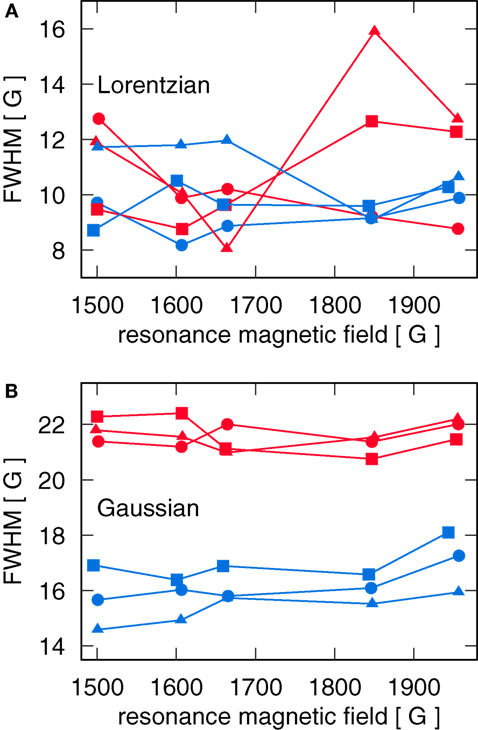
Figure 4. Anisotropic full width at half maximum (FWHM) of EDMR signals for the Lorentzian (A) and Gaussian (B) components. The three red and blue lines are for the results for three device elements with θ = 0° and 90°, respectively.
The Lorentzian components are almost insensitive to magnetic field strength for both θ = 0° and 90° (Figure 4A). Based on the fact that the Lorentzian component is attributable to mobile carriers, we conjecture that the anisotropic g-value can be averaged by carrier motion.
These results suggest that the spin-dependent processes investigated here are influenced by the molecular arrangement of the pentacene through anisotropic HFI and SOC. However, the degree of this influence varies with the mobility of the relevant carriers, with the molecular arrangement having a weak effect in the case of mobile carriers but a strong one for trapped carriers.
Since fluctuations in HFI and SOC generate a random local magnetic field, they play a role in the mixing of singlet states with triplet states (Yu, 2012). Therefore, these magnetic interactions can be important for spin-dependent recombination processes of excitons in organic light-emitting diodes or in solar cells. Additionally, carrier transport phenomenon in electronic devices, particularly organic devices, may be influenced by so-called Pauli spin blockade (Bobbert et al., 2007; Danon et al., 2013).
Furthermore, HFI are also important in experimental investigations of molecular dynamics, since carrier spin can be influenced by molecular dynamics, and the latter should involve nuclear spin motion through HFI. We predict that variable-temperature/angle mf-EDMR measurements could become a valuable tool for probing molecular dynamics in electronic/spintronic devices.
SOC is at the origin of the spin Hall effect (SHE), which allows the production of pure spin currents (Kato et al., 2004), and molecular arrangements are important in this context because spatially inhomogeneous SOC due to molecular disorder is likely to lead to deterioration of the spin current (Majumdar and Majumdar, 2012). We also suggest that for realization of the inverse spin Hall effect (ISHE) in pentacene-based devices, a high degree of orientation of the pentacene molecules in the direction of the spin-current flow is desirable. For spintronic applications of pentacene, such as generation of spin currents by SHE and their detection by ISHE, its crystallinity along the direction of carrier transport and spin flow should be taken into account.
We now turn to the relevance of our results to the conduction efficiency of spin currents. The carrier transport mechanism in our polycrystalline based PSBD should be thought of as hopping rather than band-like conduction. For hopping transport of carriers in an organic semiconductor, the higher mobility resulting from improved crystallinity increases the degree of exposure of carrier spins to magnetic interaction. Thus, the effects of an increased diffusion coefficient (i.e., increased mobility) of carriers could be canceled by the increased exposure to magnetic interaction (Yu, 2012; Watanabe et al., 2014). Therefore, from the perspective of spin-current applications of pentacene, although the in-plane mobility due to π-stacking is higher than the out-of-plane mobility, it is crucial that spin states be de-mixed via the magnetic interaction rather than via the differences in mobility.
In this article, we have supposed that the spin dependence of electrical conduction in pentacene results from hindrance of carrier transport due to the Pauli spin blockade effect of the precursor triplet state produced by pairs of mobile and trapped positive polarons. Since, for trapped carriers, spin relaxation by SOC with electron scattering is reduced, the spin states of the trapped carriers should persist for long times (Watanabe et al., 2014). The high spin-current flow in pentacene makes Pauli spin blockade more likely, and consequently decreased carrier mobility should lead to a reduced spin current. Since trapped sites probably exist in the disordered regions in pentacene thin films, spin-current flow in the out-of-plane direction should be more favored than in-plane flow. In addition, to improve the spin-current flow, the use of highly crystalline pentacene with fewer disordered regions at the grain boundaries would be desirable.
The results of the spectral decomposition indicate that signal intensity for the Gaussian component is larger than that for the Lorentzian (Figure 3; see Figures S1–S3 in Supplementary Material). We infer from this that more trapped polarons are participating Pauli spin blockade than mobile polarons. Furthermore, we found that the Lorentzian lines for θ = 0° give smaller signal than those for θ = 90°. This may be due to anisotropic relaxation time of the Lorentzian lines. Generally, electronic spins with the longer spin relaxation time are easier to saturate using continuous-wave microwave irradiation than those with the short relaxation time. At the same time, the larger time-fluctuation in local field perpendicular to an external magnetic field causes the smaller longitudinal (T1) spin relaxation time. In our case, for the configuration of θ = 0°, the fluctuation of local field around a pentacene molecule is likely to be generated in the x- and z-directions, which is originated from g-factor value fluctuated over the range between gx and gz. This is due to random reorientation of the principal axis system (PAS) of g-tensor between x- and z-directions during carrier hopping transport between crystalline grains, of which transport is along y-direction. Eventually the fluctuation in the x–z-plane accelerates the spin relaxation, which leads to fast spin relaxation for the Lorentzian component and difficulty in magnetization saturation by microwave irradiation. By contrast, for the configuration of θ = 90°, time-fluctuation of local field is produced by random reorientation of the PAS of g-tensor in the perpendicular projection component of the x–z-plane to the direction of external magnetic field. The fluctuation of the y-direction is negligible because of molecular arrangement of pentacene fixed to y-direction. Therefore the fluctuation of local field for θ = 90° should be smaller than that for θ = 0°. The difference in saturation efficiency between two configurations gives smaller EDMR signal for θ = 0° than for θ = 90°.
It is also worth noting that although our EDMR measurements were carried out in the trap-free SCLC regime, the spin-dependent processes were detected by trapped carriers; in other words, a quasi-equilibrium-like situation was experimentally confirmed by the EDMR measurements, suggesting that this EDMR method could become a valuable probe for trapped states.
The likely existence of trapped carriers in the disordered regions means that the spin-dependent processes observed in our device should reflect the effect of molecular arrangements through the trapped-carrier EDMR signal. By contrast, for solar cell applications, where the dominant spin-dependent process is probably recombination, the EDMR signal of the photocurrent should reflect the effects of the molecular arrangements not only in the disordered regions but also in the crystalline grains. In the grains, a greater degree of anisotropy is likely because crystalline regions of molecular semiconductors generally exhibit a higher degree of order than do disordered regions. We, therefore, believe that it should be possible to study molecular arrangements in the crystalline grains and the disordered regions independently via measurements of different spin-dependent processes. Furthermore, it may be possible to determine the influence of anisotropic magnetic interactions on carrier spins both inside and outside grains.
Conclusion
We have studied the influence of molecular arrangements on spin-dependent space-charge-limited conduction in a pentacene Schottky barrier diode using spectral analysis of the anisotropy of mf-EDMR spectra. These EDMR spectra can be decomposed into two components due to mobile and trapped polarons, respectively. We have also analyzed the dependence of the linewidth and the degree of anisotropy on the resonance magnetic field for the two components. To the best of our knowledge, this article is the first to describe how the EDMR linewidth reflects pentacene molecular arrangements and how these arrangements affect spin-dependent electrical conduction. We have also shown that angle-dependent mf-EDMR measurements can provide information about the influence of molecular arrangements on electrical conduction and that it is necessarily to consider these arrangements in the structural design of devices. Complex molecular systems such as π-conjugated polymers often show polymorphic behavior, leading to a variety of complex effects on the phenomena studied here, and these should be the subject of future studies.
Author Contributions
KF conceived the experimental work and contributed to data analysis and manuscript preparation. NA conceived the study, revised the manuscript, and supervised the work. Both authors read and approved the final manuscript. All appropriate permissions have been obtained from the copyright holders of any work that has been reproduced in the manuscript.
Conflict of Interest Statement
The authors declare that the research was conducted in the absence of any commercial or financial relationships that could be construed as a potential conflict of interest.
Acknowledgments
The authors thank Professors Takeshi Yamanobe and Hiroki Uehara at Gunma University for allowing us to use the X-ray diffractometer.
Funding
This work was supported by the Japan Society for the Promotion of Science (JSPS) KAKENHI Grant-in-Aid for Challenging Exploratory Research Number 21350125.
Supplementary Material
The Supplementary Material for this article can be found online at http://journal.frontiersin.org/article/10.3389/fmats.2017.00024/full#supplementary-material.
References
Ando, K., Watanabe, S., Moose, S., Saitoh, E., and Sirringhaus, H. (2013). Solution-processed organic spin-charge converter. Nat. Mater. 12, 622–627. doi: 10.1038/nmat3634
Baker, W. J., Ambal, K., Waters, D. P., Baarda, R., Morishita, H., van Schooten, K., et al. (2012). Robust absolute magnetometry with organic thin-film devices. Nat. Commun. 3, 898. doi:10.1038/ncomms1895
Behrends, J., Schnegg, A., Lips, K., Thomsen, E., Pandey, A., Samuel, I., et al. (2010). Bipolaron formation in organic solar cells observed by pulsed electrically detected magnetic resonance. Phys. Rev. Lett. 105, 176601. doi:10.1103/PhysRevLett.105.176601
Bobbert, P., Nguyen, T., Van Oost, F., Koopmans, V., and Wohlgenannt, M. (2007). Bipolaron mechanism for organic magnetoresistance. Phys. Rev. Lett. 99, 216801. doi:10.1103/PhysRevLett.99.216801
Danon, J., Wang, W., and Mancho, A. (2013). Pauli spin blockade and the ultrasmall magnetic field effect. Phys. Rev. Lett. 111, 066802. doi:10.1103/PhysRevLett.111.066802
Fukuda, K., and Asakawa, N. (2016). Development of multi-frequency esr/edmr system using a rectangular cavity equipped with waveguide window. Rev. Sci. Instrum. 87, 113106. doi:10.1063/1.4967712
Fukuda, K., and Asakawa, N. (2017). Spin-dependent electrical conduction in a pentacene schottky diode explored by electrically detected magnetic resonance. J. Phys. D Appl. Phys. 50, 055102. doi:10.1088/1361-6463/aa524b
Gershenson, M., Podzorov, V., and Morpurgox, A. (2006). Electronic transport in single-crystal organic transistors. Rev. Mod. Phys. 78, 973. doi:10.1103/RevModPhys.78.973
Honsho, Y., Miyakai, T., Sakurai, T., Saeki, A., and Seki, S. (2013). Evaluation of intrinsic charge carrier transport at insulator-semiconductor interfaces probed by a non-contact microwave-based technique. Sci. Rep. 3, 3182. doi:10.1038/srep03182
Joshi, G., Miller, R., Ogden, L., Kavand, M., Jamali, S., Ambal, K., et al. (2016). Separating hyperfine from spin-orbit interactions in organic semiconductors by multi-octave magnetic resonance using coplanar waveguide microresonators. Appl. Phys. Lett. 109, 103303. doi:10.1063/1.4960158
Kato, Y., Myers, R., Ossard, A., and Awschalom, D. (2004). Observation of the spin hall effect in semiconductors. Science 306, 1910–1913. doi:10.1126/science.1105514
Kim, T.-S., Kim, S. H., Jang, M., Yang, H., and Lee, T.-W. (2014). Charge transport and morphology of pentacene films confined in nano-patterned region. NPG Asia Mater. 6, e91. doi:10.1038/am.2014.3
Köhler, J., Disselhorst, J., Donckers, M., Groenen, E., Schmidt, J., and Moerner, W. (1993). Magnetic resonance of a single molecular spin. Nature 363, 242. doi:10.1038/363242a0
Krinichnvi, V., Roth, H.-K., and Konkin, A. (2004). Multifrequency EPR study of charge transfer in poly(3-alkylthiophenes). Phys. B 344, 430. doi:10.1016/j.physb.2003.10.024
Lee, J. Y., Roth, S., and Park, Y. (2006). Anisotropic field effect mobility in single crystal pentacene. Appl. Phys. Lett. 88, 252106. doi:10.1063/1.2216400
Majumdar, S., and Majumdar, H. (2012). Decay in spin diffusion length with temperature in organic semiconductors-an insight of possible mechanisms. Synth. Met. 173, 26–30. doi:10.1016/j.synthmet.2013.02.002
Malissa, H., Kavand, M., Waters, D., Van Schooten, K., Burn, P., Vardeny, Z., et al. (2014). Room-temperature coupling between electrical current and nuclear spins in oleds. Science 345, 1487–1490. doi:10.1126/science.1255624
Marumoto, K., Kuroda, S. I., Takenobu, T., and Iwasa, Y. (2006). Spatial extent of wave functions of gate-induced hole carriers in pentacene field-effect devices as investigated by electron spin resonance. Phys. Rev. Lett. 97, 256603. doi:10.1103/PhysRevLett.97.256603
Mattheus, C. C., Dros, A. B., Baas, J., Oostergetel, G. T., Meetsma, A., de Boer, J. L., et al. (2003). Identification of polymorphs of pentacene. Synth. Met. 138, 475–481. doi:10.1016/S0379-6779(02)00467-8
McCamey, D., Seipel, H., Paik, S., Walter, M., Borys, N., Lupton, J., et al. (2008). Spin rabi flopping in the photocurrent of a polymer light-emitting diode. Nat. Mater. 7, 723. doi:10.1038/nmat2252
Mizoguchi, K. (1995). Spin dynamics study in conducting polymers by magnetic resonance. Jpn. J. Appl. Phys. 34, 1. doi:10.7567/JJAP.34.1
Morton, J. (1964). Electron spin resonance spectra of oriented radicals. Chem. Rev. 64, 453–471. doi:10.1021/cr60230a005
Nakayama, Y., Mizuno, Y., Hikasa, M., Yamamoto, M., Matsunami, M., Ideta, S., et al. (2017). Single-crystal pentacene valence-band dispersion and its temperature dependence. J. Phys. Chem. Lett. 8, 1259. doi:10.1021/acs.jpclett.7b00082
Noe, G., Nojiri, H., Lee, J., Woods, G., Léotin, J., and Kono, J. (2013). A table-top, repetitive pulsed magnet for nonlinear and ultrafast spectroscopy in high magnetic fields up to 30 T. Rev. Sci. Instrum. 84, 123906. doi:10.1063/1.4850675
Sakai, K., Okada, Y., Uemura, T., Tsurumi, J., Häusermann, R., Matsui, H., et al. (2016). The emergence of charge coherence in soft molecular organic semiconductors via the suppression of thermal fluctuation. NPG Asia Mater. 8, e252. doi:10.1038/am.2016.30
Sakanoue, T., and Sirringhaus, H. (2010). Band-like temperature dependence of mobility in a solution-processed organic semiconductor. Nat. Mater. 9, 736. doi:10.1038/nmat2825
Sanvito, S., and Dediu, V. (2012). Spintronics: news from the organic arena. Nat. Nanotechnol. 7, 696–697. doi:10.1038/nnano.2012.197
Seck, M., and Wyder, P. (1998). A sensitive broadband high-frequency electron spin resonance/electron nuclear double resonance spectrometer operating at 5–7.5 mm wavelength. Rev. Sci. Instrum. 69, 1817–1822. doi:10.1063/1.1148847
Shimoi, Y., Marumoto, K., and Kuroda, S. (2012). Theoretical ESR g values in rubrene and oligoacenes. Mol. Cryst. Liq. Cryst. 566, 33–37. doi:10.1080/15421406.2012.701113
Silva, G., Santos, L., Faria, R., and Graeff, C. (2001). Edmr of Meh-Ppv LEDs. Phys. B 308, 1078–1080. doi:10.1016/S0921-4526(01)00859-6
Sun, D., van Schooten, K., Kavand, M., Malissa, H., Zhang, C., Groesbeck, M., et al. (2016). Inverse spin hall effect from pulsed spin current in organic semiconductors with tunable spin-orbit coupling. Nat. Mater. 15, 863–869. doi:10.1038/nmat4618
Takeda, K., Takegoshi, K., and Terao, T. (2001). Dynamic nuclear polarization by photoexcited-triplet electron spins in polycrystalline samples. Chem. Phys. Lett. 345, 166–170. doi:10.1016/S0009-2614(01)00840-5
Tani, Y., Teki, Y., and Shikoh, E. (2015). Spin-pump-induced spin transport in a thermally evaporated pentacene film. Appl. Phys. Lett. 107, 242406. doi:10.1063/1.4938132
Tateishi, K., Negoro, M., Nishida, S., Kagawa, A., Morita, Y., and Kitagawa, M. (2014). Room temperature hyperpolarization of nuclear spins in bulk. Proc. Natl. Acad. Sci. U.S.A. 111, 7527. doi:10.1073/pnas.1315778111
Thorsmølle, V., Averitt, R., Demsar, J., Smith, D., Tretiak, S., Martin, R., et al. (2009). Morphology effectively controls singlet-triplet exciton relaxation and charge transport in organic semiconductors. Phys. Rev. Lett. 102, 017401. doi:10.1103/PhysRevLett.102.017401
Voz, C., Puigdollers, J., Martin, I., Munoz, D., Orpella, A., Vetter, M., et al. (2005). Optoelectronic devices based on evaporated pentacene films. Sol. Energy Mater. Sol. Cells 87, 567–573. doi:10.1016/j.solmat.2004.07.039
Watanabe, S., Ando, K., Kang, K., Mooser, S., Vaynzof, Y., Kurebayashi, H., et al. (2014). Polaron spin current transport in organic semiconductors. Nat. Phys. 10, 308–313. doi:10.1038/nphys2901
Westermeier, C., Cernescu, A., Amarie, S., Liewald, C., Keilmann, F., and Nickel, B. (2014). Sub-micron phase coexistence in small-molecule organic thin films revealed by infrared nano-imaging. Nat. Commun. 5, 4101. doi:10.1038/ncomms5101
Yang, S., Shin, K., and Park, C. (2005). The effect of gate-dielectric surface energy on pentacene morphology and organic field-effect transistor characteristics. Adv. Funct. Mater. 15, 1806–1814. doi:10.1002/adfm.200400486
Keywords: spintronics, electrically detected magnetic resonance, organic semiconductor, morphology, electron spin resonance, spin-dependent process, polaron, pentacene
Citation: Fukuda K and Asakawa N (2017) Angular-Dependent EDMR Linewidth for Spin-Dependent Space-Charge-Limited Conduction in a Polycrystalline Pentacene. Front. Mater. 4:24. doi: 10.3389/fmats.2017.00024
Received: 19 May 2017; Accepted: 31 July 2017;
Published: 14 August 2017
Edited by:
Alexey A. Sokol, University College London, United KingdomReviewed by:
Chang-Yong Nam, Brookhaven National Laboratory, United StatesAyelet Vilan, Weizmann Institute of Science, Israel
Constantinos Simserides, National and Kapodistrian University of Athens, Greece
Copyright: © 2017 Fukuda and Asakawa. This is an open-access article distributed under the terms of the Creative Commons Attribution License (CC BY). The use, distribution or reproduction in other forums is permitted, provided the original author(s) or licensor are credited and that the original publication in this journal is cited, in accordance with accepted academic practice. No use, distribution or reproduction is permitted which does not comply with these terms.
*Correspondence: Naoki Asakawa, YXNha2F3YUBndW5tYS11LmFjLmpw