 Mark Buckwell
 Wing H. Ng
 Stephen Hudziak
 Adnan Mehonic
 Mario Lanza
 Anthony J. Kenyon
- 1Department of Electronic and Electrical Engineering, University College London, London, United Kingdom
- 2Institute of Functional Nano and Soft Materials Collaborative Innovation Center of Suzhou Nanoscience & Technology Soochow University, Suzhou, China
The atomic force microscope (AFM) empowers research into nanoscale structural and functional material properties. Recently, the scope of application has broadened with the arrival of conductance tomography, a technique for mapping current in three-dimensions in electronic devices by gradually removing sample material with the scanning probe. This technique has been valuable in studying resistance switching memories and solar cells, although its broader use has been hindered by a lack of understanding of its reliability and practicality. Implementation can be preclusive, owing to difficulties in characterizing tip-sample interactions and accounting for probe degradation, both of which are crucial factors in process efficacy. This work follows the existing conductance tomography literature, presenting an insight into the repeatability and reliability of the material removal processes. The consistency of processes on a hard oxide and a softer metal are investigated, to understand the critical differences in etching behavior that might affect tomography measurements on heterostructures. Individual probe behavior stabilizes following a wearing-in stage and etching processes are consistent between probes, in particular on oxide. However, process inconsistency increases with applied force on metal. The effects of scan angle, tip speed and feedback gain are therefore explored and their tuning found to improve the spatial consistency of material removal. With these findings, we aim to present a critical study of the implementation of tomography with the AFM in order to contribute to its methodological development.
Introduction
The atomic force microscope (AFM) is a powerful tool, enabling high resolution imaging of a wide variety of surfaces (Yang et al., 1994; Ikai, 1996; Lanza et al., 2017). In addition, a range of operational modes are available for mapping information on surface mechanics (Bruker Nano Surfaces, 2018) and chemistry (García and Perez, 2002), as well as other properties such as conductivity (Pan et al., 2017). Thus, with the advancement of micro- and nanoscale technologies, AFM has offered significant insight in materials research (Gerber and Lang, 2006; Hui and Lanza, 2019). For example, conducive AFM has been of particular importance in such fields as resistance switching memories (Brivio et al., 2014; Lanza, 2014; Bousoulas et al., 2015; Mehonic et al., 2016) and energy harvesting, storage and generation systems (Lanza et al., 2014; Tennyson et al., 2017), and the investigation of broader functional material properties such as charge trapping (Porti et al., 2005; Polspoel and Vandervorst, 2007), leakage (Lanza et al., 2012; Pirrotta et al., 2013), breakdown (O'Shea et al., 1995), and reliability (Porti et al., 2007).
AFM may also be used to fabricate nanoscale structures using techniques often referred to, with or without the prefix “tip-based,” (Kawasegi et al., 2006; Bourne et al., 2010; Ren et al., 2016) or “nano,” as lithography (Ogino et al., 2008), machining (Yan et al., 2015), manufacturing (Fang et al., 2017), or scratching (Huang et al., 2011). Typically, patterns are fabricated either by applying a high normal loading force to the surface to remove material or by using an electrical bias to inject or collect current and so induce material restructuring (i.e., by local anodic oxidation) (Xie et al., 2006; Garcia et al., 2014). Structures produced may be sub-10 nm (Rolandi et al., 2002), such as nanodot (Yan et al., 2015) and quantum dot arrays (Ogino et al., 2008), and channels for use in solar cells and nanochannels for fluidics (Geng et al., 2013).
Recently, conductive AFM has been combined with nanomachining in order to perform conductance tomography, mapping electrical current as material is worn from the sample (Buckwell et al., 2015a; Celano and Vandervorst, 2017). Whereas nanofabrication requires high loading forces to rapidly machine structures, material must be removed more slowly and controllably during tomography, such that a high depth resolution is achieved through films tens to hundreds of nanometers thick (Celano et al., 2018). As such, relatively low loading forces are employed, typically in the range of a few micronewtons using boron-doped diamond probes. This technique is attractive in studying the structure and function of nanoscale devices with spatially inhomogeneous conductive properties. For example, we, and others, have successfully revealed the structure of conductive filaments in resistance switching devices (Celano et al., 2014; Buckwell et al., 2016; Hammock, 2017) and the technique has also been applied to map charge conduction pathways in solar cells (Luria et al., 2016) and nanofabricated insulating structures in organic electronics (Kamaludin et al., 2018). However, little work has been done to assess the material processing involved and we note that the methodology has yet to proliferate significantly, despite the successful and interesting work in the literature. This leads us to consider that studies of reliability and practicality would be useful contributions to building experimental frameworks for performing tomography.
It is generally assumed that the apices of the diamond-tipped probes used in AFM tomography and lithography do not change significantly during etching because diamond is extremely hard. However, boron doping has been shown to reduce the hardness and increase the wear rate of diamond (Buijnsters et al., 2016). This effect is more pronounced at heavier doping levels, such as would be required to produce highly conductive diamond AFM probes. Therefore, it is reasonable to expect such probes to be susceptible to wear during etching. Measurable probe damage has previously been reported, implying that the apex geometry will change over time (Khurshudov et al., 1996; Chen et al., 2018). Wear has previously been noted as a result of etching crystalline silicon at 60 μN (Khurshudov et al., 1996) and severe blunting of a diamond-coated probe has been demonstrated following the application of 100 μN to a dichromium nitride film (Huang et al., 2012). Conversely, we are unable to find detailed reports of wear resulting from etching oxides and metals, or the practical implications for tomography measurements made using at least an order of magnitude lower applied force. Furthermore, it is significant that oxygen can induce amorphization of diamond, leading to wear (Peguiron et al., 2016). Oxides necessarily contain oxygen, and many materials will at least contain some trace oxygen, so this wear process might be typical of tomography. Some samples have also been reported to undergo morphological changes (Chen et al., 2018). Thus, both the sample and probe might change during measurements; it is crucial to better understand these effects in order to develop the technique and broaden its application.
As conductance tomography is not fully understood and we are yet to discern the limits of its implementation, it is important to briefly discuss its merit in comparison to alternative nanoscale probing techniques. The major strengths of performing tomography with a conductive AFM are the field of view, spatial resolution, and conductivity contrast. Typically, nanoscale features within thin films are studied using cross-sectional transmission electron microscopy. This offers excellent resolution, but sample preparation can be difficult if the exact location of the feature(s) of interest is not known. In addition, the imaging contrast can be poor if the composition of these features is not sufficiently distinct from the surrounding material (Duchamp et al., 2016). This contrast challenge is also true of some high-resolution techniques, such as x-ray tomography or phase contrast imaging. Using conductive AFM, we can study a large surface area to find the region of interest and subsequently zoom in to study the feature(s). We may readily resolve features whose conductive properties vary from their surroundings, even if their composition does not. For example, we have revealed the structure of conductive regions in thin silicon suboxide films, wherein the contrast results from small variations in stoichiometry and density (Buckwell et al., 2015a; Mehonic et al., 2016). These advantages have been further demonstrated in visualizing photocurrent in a solar cell under illumination, in which 20 nm spatial resolution is achieved over tens of micrometers (Luria et al., 2016). Thus, conductance tomography is a valuable technique for spatially studying electrical changes in devices.
In this work, we look at processing consistency and variation when etching nominally hard and soft samples with diamond-tipped probes. To this end, we chose silicon-rich silicon oxide, SiOx, and gold as representative materials that might be found in electronic device heterostructures (Yao et al., 2012; Mehonic and Kenyon, 2016; Mehonic et al., 2016, 2018; Munde et al., 2017; Ng et al., 2018). We study the repeatability of processes with a single probe and between different probes. Additionally, we investigate the differences in processing between SiOx and gold. Given that many devices have neighboring layers (Celano et al., 2014; Mehonic et al., 2017) or embedded structures (Schulze et al., 2012; Stan et al., 2016) whose mechanical properties might vary significantly, it is critical to understand how a tomography measurement might progress through multiple materials. We therefore study the roughness of the trench that we etch, in order to assess whether the base of the sampling volume would be sufficiently smooth to gather accurate tomography information. Furthermore, we use scanning electron microscopy (SEM) to assess the condition of probes that have been used in etching processes. Thus, we are able to some degree to assess probe degradation. The aim of this work is not to present a comprehensive and definitive characterization and model for tomography processes. Rather, we draw together our observations from a variety of measurements in order to critique the reliability of the method. Thus, we hope to contribute to the development of AFM tomography and facilitate its further use as a materials research tool.
Materials and Methods
Samples were fabricated on a silicon wafer topped by 1 μm of thermally grown SiO2. Firstly, 200 nm of molybdenum was deposited by sputtering. Subsequently, 40 nm of SiOx was deposited by reactive sputtering. Hundred nanometer gold was then deposited by electron beam evaporation, with 5 nm titanium used as an adhesion layer. A shadow mask was used to produce squares of metal on the SiOx, with sizes from 200 μm × 200 μm to 800 μm × 800 μm. Thus, both SiOx and gold layers were available for etching processes on the same sample. Our layers had roughnesses around 1 and 1.3 nm for SiOx and gold, respectively.
AFM measurements were made with a Bruker Icon microscope using Bruker Nanoscope software, DDESP-V2 probes (diamond-coated, Bruker) and SSRM-DIA probes (full-diamond, IMEC). The normal force applied by the probe was estimated from the deflection sensitivity using Hooke's law (Palacio and Bhushan, 2010), corrected to account for the cantilever tilt (Ohler, 2007), where the spring constant, k, was determined according to:
where kn and fn are the nominal spring constant and resonant frequency of the probe as quoted by the manufacturer and f is its measured resonant frequency (Sarid, 1991).
For consistency, we applied no voltage between the sample and the scanning probe and we used gain settings that were well-suited for imaging measurements during all etching processes, except where stated. 2 μm × 2 μm scans used 256 scan lines, for a feed (separation between scan lines) of 7.8 nm. 5 μm × 5 μm scans used 512 scan lines, for a feed of 9.8 nm. Note that we did not investigate the effect of feed as it has been studied previously (Fang et al., 2006; Guo et al., 2017; Celano et al., 2018). Our feeds were chosen for a favorable compromise between spatial resolution, material removal rate (removing sufficient material to profile through the sample in a reasonable time) and trench smoothness. We chose a desirable spatial resolution to be a pixel size below 10 nm × 10 nm, based on the size of details in the conductive features we have previously observed with this method (Buckwell et al., 2015a). Trench smoothness corresponds to minimizing the depth of grooves parallel to the fast scan axis of the probe. For clarity, this axis is parallel to the trace/retrace movement of the probe. The scan angle is defined as the angle between fast scan axis and the long axis of the cantilever. Thus, scanning or etching at 90° indicates that the trace/retrace movement is perpendicular to the long axis of the cantilever. Etching was performed at 90° with a scan rate of 1 Hz (i.e., a tip speed of 4 μms−1 for a 2 μm × 2 μm scan area) unless otherwise stated.
Except where discussed, etching processes were set up by firstly contacting the sample surface with a low applied force and then pausing the probe movement at one or other end of the slow scan axis. The deflection setpoint was then increased to reach the desired applied force and the probe movement resumed to begin etching. We define an etching pass as a scan over the sampling area with sufficient applied force to cause material removal. That is, three etching passes corresponds to consecutively scanning the same sampling area three times with a high loading force. Following the final etching pass, scanning was paused and the setpoint reduced to apply a low force, suitable for imaging. The scan size was then increased and the scan angle rotated by 90° to take an image of the etched trench.
All data were processed using Nanoscope Analysis. For each etching process, the depth was quantified from the larger area image of the etched trench. The data were leveled and the step height function used to measure the mean height difference between the non-etched areas at the edges of the image and the base of the trench. The sloped edges of the trench were avoided, as were any large pieces of debris that might affect the measurement. In this work we discuss the trench roughness with respect to the initial surface roughness, unless otherwise stated. This roughness change as a result of etching was quantified by measuring the roughness difference between the base of the trench and the non-etched areas surrounding it. Thus, negative values constitute smoothing and positive values roughening. In all cases we discuss the root-mean-square roughness. The trench roughness, rather than the roughness change, was used as the error on the etch depth. The standard deviation of the roughness, measured on four non-etched areas surrounding the trench, was used as the error on the roughness change. We note here that the error bars on the roughness change are often too small to observe. Where we have fitted data we quote the coefficient of determination, R2, as a measure of the goodness of fit.
SEM images were taken using Zeiss XB-1540 CrossBeam field instrument. The acceleration voltage used for imaging varied between 3 and 10 kV. Unless otherwise stated as top-down images, probes were tilted at 45° to image their apices and the images height-corrected to account for this. Our estimates of the radius of curvature, r, may therefore suffer from inaccuracies due to the viewing angle, though we only intend them as a qualitative measure.
Results and Discussion
Process Consistency for Single Probes
Repeatability and the effect of probe condition are principal concerns for tomography processes, thus we sought to determine the consistency of etching behavior with individual diamond-coated and full-diamond probes. We performed sequences comprising twelve sets of three etching passes on 2 μm × 2 μm areas of SiOx, each set at a fresh location. We additionally studied the changes in performance over time at low and high forces. Using the same pair of setpoints for each probe, alternating between locations, the diamond-coated probe forces were 2.1 and 6.4 μN and the full-diamond probe forces 0.5 and 1.5 μN. Notably, the pair of forces used with the full-diamond probe are both lower, so we would expect smaller etch depths and less pronounced, if any, wear.
In Figure 1, we observe that the etch depth for the diamond-coated probe decreases slightly over the first three locations. Following this, both high and low forces consistently etch around 90% of their initial depth. Conversely, for the full-diamond probe the depth increases for the first three locations before becoming steady at around 120% of the initial value at both forces. For both probes, in particular for the higher force scans, the roughness of the etched trench decreases as the probe is used more (i.e., a more negative roughness change), becoming steadier with time. Notably, the error bars are quite large at up to around ±1 nm, particularly in comparison to the etch depth at lower force. The SiOx has an initial roughness of around 1 nm, so the error values reflect this starting value, reduced by the probe smoothing the trench.
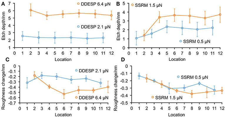
Figure 1. The effect of probe history on the consistency of etching processes on SiOx. (A,B) Etch depths at each location for the diamond-coated (DDESP) and full-diamond (SSRM) probes, respectively. The etch depth initially decreases for the diamond-coated probe, whereas it increases for the full-diamond probe. (C,D) Trench roughness change for the diamond-coated and full-diamond probes, respectively. The trenches become smoother with probe use.
Stabilization of etching behavior (i.e., the etch rate) has previously been related to wear of a fresh probe apex during the first stages of etching (Huang et al., 2012). It is likely that fragile asperities, initially dominating the tip-sample contact, are removed, exposing more robust material (Arda Gozen and Burak Ozdoganlar, 2014). Thus, the probe condition stabilizes. Alternatively, instrumental relaxation over time might produce a gradual drift; we noted a 2% decrease in the deflection sensitivity following etching, which would reduce the force applied for a steady setpoint voltage by the same proportion. Other than this, in this work we noted no significant deviations in the cantilever resonant frequency or deflection sensitivity.
Figures 2A,B show SEM images of an unused diamond-coated probe and the probe used for the processes shown in Figure 1. There is a small amount of debris around the tip but the apex is still visible. Interestingly, the used probe in Figure 2B is sharper (i.e., it has a smaller radius of curvature, r) than the new probe in Figure 2A. However, it should be noted that we observed variability in the sharpness of new probes, with r from around 120 to 165 nm (Supplementary Figure 1). Generally, though, new probes demonstrate the presence of multiple grains at the apex. The apex of the probe in Figure 2B shows a reduction in the presence of grainy features compared to the probe in Figure 2A. We suppose that sharp apices of grains initially present have been worn away, leaving a smoother apex, though it is not significantly blunted. This would be expected given the stabilization of the etch rate, as discussed above. Thus, etching behavior might change as the tip-sample contact area increases; for the same applied force the pressure will be lower. The increasing smoothing of the etched area over time shown in Figures 1C,D also supports this; a slightly blunted probe with a larger sample contact area should produce wider, shallower grooves.
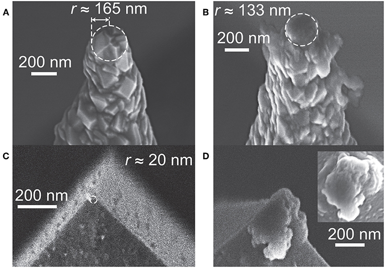
Figure 2. SEM images of unused and used diamond-tipped probes, taken following the processes in Figure 1. (A,B) New and used diamond-coated probes, respectively. The new probe has a radius of curvature, r, around 165 nm, highlighted by the dashed circle. Debris has accumulated on the tip of the used probe, though the apex is not obscured. It also appears blunted, with less well-defined grains, although it is sharper (i.e., has a lower r) than the new probe. (C,D) New and used full-diamond probes, respectively. Initially, the full-diamond probe is sharper than the diamond-coated probe; r is difficult to determine from the image, though we have estimated it to be 20 nm. Following use, the apex appears obscured by debris, so it is difficult to discern whether it is blunt. Inset—top-down view of the probe in (D); the apex is entirely obscured by debris. Note that for both probe types the unused probes are representative and are not the same probes used for etching processes.
The contrasting behavior between the probe types is interesting. It is straightforward to consider that a probe might remove material less effectively as the apex is worn. However, it is less clear how the etch rate of a probe might increase with use, as in the case of the full-diamond probe. Changes in etch rate have previously been observed for used full-diamond probes, attributed to particle attachment and detachment at the apex during etching (Chen et al., 2018). As shown in Figures 2B,D, debris accumulated at the apex probes during etching, so particle attachment certainly seems possible. However, the apex appears obscured in Figure 2D, yet we observed an increasing etch rate. Thus, we suppose that loose particles might attach to the apex prior to etching, subsequently detaching and so affecting the probe sharpness and therefore the etch rate. Debris might also accumulate as the probe is retracted from the sample; it is not possible to know the condition of the apex during etching as this necessarily means the tip and sample lose contact, allowing particulates to adhere to the probe. An alternative suggestion to particle attachment/detachment is that apex wear could produce a sharper or more optimal etching geometry, particularly as we observe a gradual increase in etch rate rather than an abrupt change that might correspond to discrete particle detachment. A report on the wear of a diamond probe over time revealed apex changes that could indicate a slight sharpening (Khurshudov et al., 1996). Therefore, we surmise that although the full-diamond probe is initially very sharp, as shown in Figure 2C, gradual wear results in an apex that more effectively removes sample material. As such, there is likely an optimum trade-off between sharpness and bluntness to maximize material removal and trench smoothing. Another possible cause of variations in etching behavior is cantilever damage, if the force applied by the probe causes either the cantilever or its reflective coating to crack. We therefore performed SEM on the backs of unused and used diamond-probes but detected no evidence of damage.
Further observations of the wear-in process are shown in Figures 3A,B. Here, a single probe is used to etch 2 μm × 2 μm areas at a range of forces. At each force, a single etching pass is made at one location, followed by a set of six passes at a new location (i.e., cycling between Figures 3A,B). The first processes are performed at around 6 μN, producing the deepest trenches. Subsequently, the force is increased from just below 1 μN to around 10 μN, producing a linear trend, even above 6 μN. This might indicate that the probe is worn-in during the first processes, producing a more robust apex that is less affected by wear, even at higher forces, though it removes material less effectively. We suggest here that measureable probe wear might occur at a threshold force; we suppose this is below 6 μN on SiOx, as the most distinct changes observed in etching follow the application of 6 μN, as shown in Figures 1, 3. Finally, we note that we are able to remove greater than or less than 1 nm depth of material per etching pass, depending on the applied force.
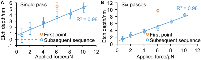
Figure 3. Wear-in process for diamond-coated probe on 2 μm × 2 μm areas of SiOx. (A,B) Etch depth for single and sets of six etching passes, respectively. At each force, firstly a single pass was made at one location, followed by a set of six passes at a new location (i.e., cycling between A,B). In each case, the first data point (orange circles) produces the deepest trench. Subsequently, measurements were made with increasing force from around 1 to 10 μN, producing a linear trend.
We repeated our measurements of probe history and etching consistency with a diamond-coated probe on the gold film. Here, we alternated between applied forces of around 1.6 and 4.7 μN, again making three etching passes at each location. The results, shown in Figures 4A,B, do not demonstrate the decrease and subsequent plateau in etch depth observed on SiOx in Figure 1. Rather, the etch depths at both applied forces fluctuate more between points. The lack of a significant change in the etching behavior suggests that the process does not affect the probe significantly. This is supported by the SEM image in Figure 4C, which indicates that grains are still present at the apex, where r is relatively small for a diamond-coated probe, around 100 nm (the smallest we observed in this work was 69 nm, as shown in Supplementary Figure 1). Thus, we surmise that apex wear, corresponding to removal of prominent grain apices, is less pronounced on gold than on SiOx.
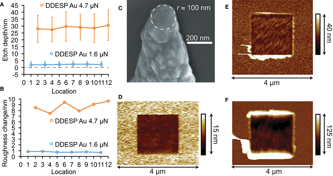
Figure 4. Consistency of etching gold and comparison with SiOx. (A,B) Etch depth and roughness change, respectively, when etching the gold sample. The etch depth fluctuates although no general trend is present. Notably, the roughness of the etched regions increases by around a third of the etch depth. (C) SEM image of the probe following the etching processes in (A,B). The probe does not appear worn as r is relatively small and grainy features are still visible at the apex. (D) AFM image of typical trench produced by the diamond-coated and full-diamond probes on SiOx. The trench is level and smooth compared to the surrounding material. (E,F) AFM images of the smoothest and roughest trenches produced on gold, at locations 11 and 12, respectively. Both of these are rougher than their surroundings and show severe wave-like patterning.
The fluctuations between data points in Figures 4A,B suggest greater etch depth and roughness variability on gold compared to SiOx. Interestingly, both forces cause a roughening effect, indicated by large error bars and positive roughness changes. To better understand the differences between processes on gold and SiOx, we looked at the topography of the etched trenches. In Figure 4D we show a typical trench produced by diamond-coated and full-diamond probes on SiOx, in which the base of the trench is quite flat and smooth, with little debris present. This is in contrast to the trenches on the gold film shown in Figures 4E,F. Here, we observe wavy topography with a large quantity of neighboring debris. The waviness of the gold trenches is most pronounced in Figure 4F, where there is a 60 nm depression in the upper half, with the lower half only around 10 nm below the surroundings. The significant roughness of the gold trenches likely results from such height variations and is undesirable for AFM tomography, as the sampling area is not planar. For example, if conductive AFM is used to sample current during tomography, the current mapping might be severely convoluted with the topography; we also seek to address this problem.
We used two fresh, diamond-coated probes to etch SiOx and gold in order to determine the trench depth and roughness correlation with the number of etching passes. For the SiOx, we wanted to minimize probe wear while removing significant material. Hence we applied 4.4 μN, as this was intermediate between the forces used for the DDESP probe in Figure 1 and below our suggested 6 μN wear threshold discussed following Figure 3. For the gold, we sought to minimize the roughening effect. Therefore, we applied 1.5 μN, just below the 1.6 μN applied in Figures 4B,C that appeared to produce relatively smoother trenches. We additionally hoped that increasing the number of passes might increase the smoothing of both samples.
Figure 5A demonstrates that the etch depth increases linearly with the number of passes for both samples. The slope of the SiOx is steeper, though this may be because greater force was applied. Interestingly, the y-intercept in each case would be >0 nm, particularly for SiOx. Thus, there is some finite minimum material removal effect; we suppose there might be some mechanical compression when etching that is most pronounced during the first pass. Notably, if we consider the variation in etch rate with the number of passes we would observe a rapid decrease in rate at low pass number, as shown in Figure 5B. This surface effect highlights the intrinsic interplay between material deformation and removal resulting from contact attrition during etching (Piétrement and Troyon, 2001; Celano et al., 2018). In any case, we question the use of material removal rates in etching, unless they are corrected in some way to account for this surface effect. In addition, probe wear might also cause the rate to change over time.
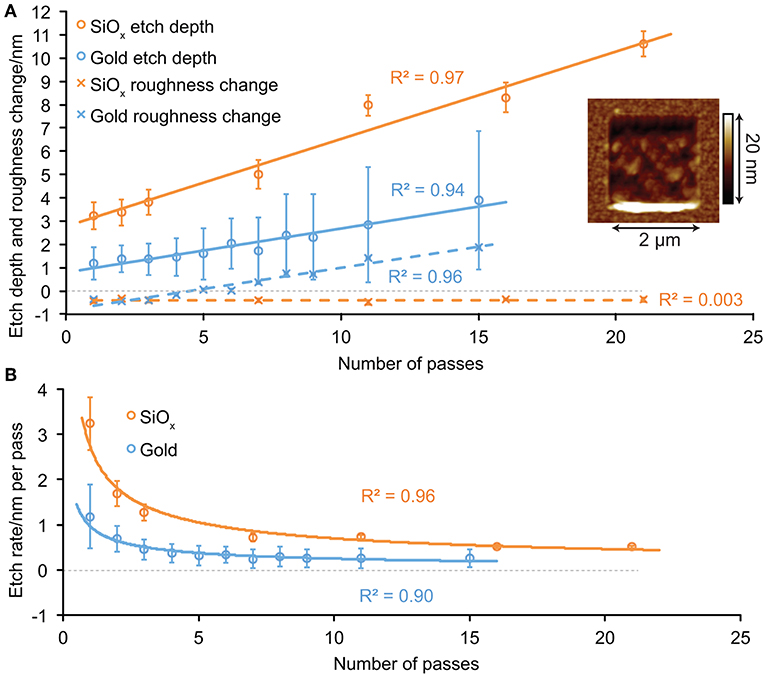
Figure 5. Etch depth and roughness change correlation with number of etching passes for diamond-coated probes applying forces of 4.4 μN on SiOx and 1.5 μN on gold. (A) The etch depth for both samples increases linearly with passes. The increasing roughness change with depth demonstrates the extent of the roughening effect on gold, whereas the SiOx is smoothed independently of the depth. Inset—topography of the trench produced from 15 passes on gold, demonstrating a deep depression at one edge extending around 10 nm below the surface. (B) The etch rate (trench depth divided by number of passes) decreases inversely with the number of passes. This is likely because there is a non-zero minimum etch depth and a linear increase of depth with number of passes, so the ratio between depth and passes diminishes.
The roughness change data in Figure 5A demonstrates a well-fitted linear trend for gold, becoming increasingly rough with the number of passes and thus with depth. This is also illustrated by the increasingly broad etch depth error bars on gold. The inset of Figure 5A demonstrates the severe conflation of the depth with roughness for the data point at 15 passes on gold. Here, the deepest part of the trench is around 10 nm, deeper than a comparable number of passes would produce at a greater force on the SiOx, but the rest of the trench is only a few nanometers deep. Evidently, roughening is a significant issue when etching gold, despite using a relatively low force and multiple passes in an attempt to smooth the trench. It is interesting that the gold data fit well with linear trends; roughening appears to scale with the number of passes. Conversely, the SiOx trenches are consistently smoothed by around 0.5 nm, although the data is poorly fitted by a linear trend. We suppose that there is a minimum roughness that is reached during etching, in this case around 0.5 nm, and the data are noisy around this value.
We finally comment on the observation in Figure 5A that all data points, aside from the SiOx roughness change, fit well with the linear trends. We surmise that this is because we applied forces lower than those observed to cause wear; if wear were occurring, we would expect the trend to be sub-linear. Thus, it appears that we were able to maintain the ability of a probe to remove material by not exceeding an applied force threshold. In fact, the apex of the probe used to etch the SiOx retained a grainy appearance, suggesting that little wear occurred. Interestingly, when studying the apices of probes following hundreds of millimeters of travel on SiOx at applied forces up to 20 μN, we observe that probes remain relatively sharp (Supplementary Figure 1). There is a large degree of debris accumulation, though this is to be expected for very large travel distances because more material is removed. However, the lack of significant blunting supports the supposition that the most pronounced probe wear occurs during the early stages of etching.
Process Consistency Between Multiple Probes
To further study process consistency and the issue of roughening the gold film, we compared processing between probes. We etched 2 μm × 2 μm areas at a range of applied forces on SiOx and gold, using three different probes on each sample (six individual probes in total). At each force, we made a single etching pass at one location and a set of six at another. We did this in order to determine the extent of the surface effect and finite minimum material removal of a single pass in comparison to multiple passes.
The aggregated trench depth data are shown in Figures 6A,B (depth and roughness for each probe are shown in Supplementary Figures 2, 3; note that we have removed two outlying data points, as discussed in the Supplementary Material). The SiOx data in Figure 6A are best fit with a linear function for both single and sets of six etching passes. In each case, greater forces produce deeper trenches. The etch depth is greater for sets of six passes than for a single pass, though only by a few nanometers. Thus, the first pass at each location again appears to produce the greatest degree of material removal. Interestingly, the data in Figure 6B for six passes on gold are best fit with an exponential function, whereas single passes best fit a linear trend, although we note that the R2 value is comparatively low. Otherwise, for both materials the etch depth is quite consistent between probes, as demonstrated by the R2 values of around 0.9. Interestingly, there is little difference between the etch depths on gold for single and sets of six passes until around 3 μN, where the variation between probes increases greatly. In particular, the data for six passes above around 3.5 μN deviates greatly from the fitted curve. This might imply that the etch depth on gold becomes increasingly unpredictable with applied force. We also note that the trench roughness is minimized around 2 μN on gold (Supplementary Figure 3), subsequently increasing rapidly with the applied force. Finally, following also our observations on Figure 5, it appears that neither increasing the number of passes nor the applied force alleviates gold roughening. The distinctly different etching trends between SiOx and gold likely indicate differences in the tip-sample contact mechanics and material removal regimes for each sample. In the case of gold, there is also a dependency on the number of etching passes. We note here that our fitting might only be appropriate to the force ranges shown in Figure 6; in particular for gold, we observed non-linearity in the single pas etch depth when more than 5 μN was applied (Supplementary Figure 4).
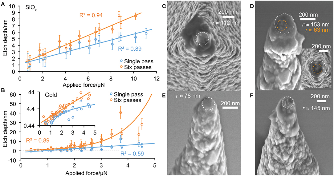
Figure 6. Etching consistency between multiple probes and SEM images of probes following use. (A) Aggregated etch depth with applied force data for single and sets of six passes on SiOx, fitted with linear functions. (B) Aggregated etch depth with applied force for gold, in which the data for single and sets of six passes have been fitted with linear and exponential functions, respectively. Inset—log y-axis plot of the same data. (C,D) Two probes following etching on SiOx. A top-down view is shown in (C). Some debris appears to have accumulated near each apex. The apex is obscured in (D), making it difficult to discern whether the larger (dashed white circle) or smaller (dashed orange circle) highlighted area corresponds to the true apex. Inset—top-down view of the apex in (D). It appears that the larger r likely describes the apex, but with multiple central protrusions present. (E,F) Two probes following etching on gold. Little debris is present and the apex in (E) appears to have less well-defined grains than an unused probe, so we suppose that wear occurs on both hard and soft samples, though more gradually for the latter.
Figures 6C–F show SEM images of some of the probes used in the etching processes of Figures 6A,B. We observe here that the probes used on SiOx show more debris accumulation than those used on gold. We also note this in Figures 2–4 (and Supplementary Figures 1, 4, 5, 7), with the trenches etched in gold showing more debris than those in SiOx; we suppose that the SiOx debris adheres to the probes and the gold debris to the trench edges.
To better understand the contrast in etching behavior between SiOx and gold, we looked at the tip-sample contact mechanics. We measured the adhesion force, deformation and energy dissipation from force-distance spectra (Bruker Nano Surfaces, 2018). All measured values are shown in Table 1. We note that the energy dissipation values are unexpectedly large, which we attribute our tip apex not being ideally hemispherical and the presence of an ambient water meniscus. However, the values in Table 1 clearly highlight qualitative differences in the interaction of the diamond probe with each sample. Firstly, the gold adheres to the probe with a greater force than does the SiOx. Secondly, the gold deforms to a greater extent under the tip, dissipating more of the energy stored by the bending cantilever. Thus, we have a clear contrast in behavior between hard and soft materials under applied forces from hard probes.
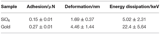
Table 1. Tip-sample contact and mechanical properties.
In consideration of the properties of Table 1 in relation to the fits in Figures 6A,B, we now endeavor to build a theoretical understanding of the tip-sample interaction during etching. We assume here that material removal results either from friction or shear strength-induced plastic flow between the two sliding contacts (Wang et al., 2012; Yang et al., 2016), or an atomistic, stress-assisted chemical process (Jacobs and Carpick, 2013).
On hard materials, such as SiOx, for etch depths that are much smaller than r, the depth has been observed to depend linearly on the applied force (Wang et al., 2011), which is in agreement with our observations in this work. Further simulations and experiments have attributed this to a linear increase in friction with applied force, as the real contact area increases (Piétrement and Troyon, 2001; Mo et al., 2009). This can be considered a multi-asperity interaction (Mo et al., 2009); the probe will make contact with sample nanoasperities of a few to tens of nanometers diameter (Buckwell et al., 2015b), creating a high contact roughness with very high pressure, of the order of tens of GPa, at each contact point. This seems appropriate to our etching processes, given that we observe multiple grains at the apices of diamond-coated probes and a sample surface with nanoscale roughness. Although the probe and sample are both hard, silica behaves in a ductile fashion at the nanoscale (Pradeep et al., 2007). Thus, at low applied forces the contact roughness enables plastic material removal with little compression. In fact, the apparent non-zero y-intercept in Figure 6A suggests that sample wear should occur even when no force is applied. This is likely due to the relatively small adhesion force between the tip and sample (Yang et al., 2016), which might induce a jump-to-contact and the onset of a repulsive wear regime as contact is made (Landman et al., 1990).
As the force applied to the SiOx is increased, there is some compression of nanoasperities, linearly increasing the real tip-sample contact area and therefore the friction. Thus, plastic material removal increases linearly with the applied force. Although we operated in ambient conditions, this multi-asperity behavior should occur even in the presence of a water meniscus because the contact roughness is maintained (Piétrement and Troyon, 2001). Here, we note a discrepancy between our observations and those in the literature. We only observe a single linear regime when etching our SiOx sample, whereas linear sliding and combined plowing and sliding regimes have been observed when etching semiconductors with full-diamond probes (Celano et al., 2018). We suppose this difference might occur because our diamond-coated probes are less sharp than full-diamond probes, thus we assume multi- rather than single-asperity contact behavior. Additionally, SiOx is an oxide and so might reasonably demonstrate different wear properties to elemental or alloyed semiconductors that are nominally oxygen-free.
For the softer gold sample, we observe two regimes. For a single etching pass, the etch depth increases linearly with applied force. We attribute this to plastic deformation of surface nanoasperities during the first pass, given the high deformation and energy dissipation values for gold in Table 1. This appears to agree with our observation that the gold surface is smoothed at lower forces (Supplementary Figure 3). Conversely, for sets of six passes, the etch depth increases exponentially, although there is little difference in depth between the data sets until around 2 μN, when the roughness also starts to increase. Additionally, as we observed in Figure 5, even at low forces the smoothing effect disappears as more etching passes are made.
The softness of the gold sample suggests that tip-sample contact may be classed as single-asperity because sample nanoasperities would readily conform to the probe apex geometry (Piétrement and Troyon, 2001). In this case, once the surface roughness has been smoothed, the contact pressure will decrease to below 1 MPa. In this regime, wear is an atomic process, with an exponential dependence on the applied force (Yang et al., 2016), which is what we observe. We therefore reason that, following an initial smoothing at low applied forces or for single passes, the gold behaves in a liquid-like manner (Merkle and Marks, 2008; Aghababaei et al., 2016), readily deforming as atomic wear progresses. In addition, the applied force might create a pile-up of material around the probe (Li et al., 2016). In combination, as the applied force and number of passes is increased, these effects produce deep depressions in the gold film but also significantly increase its roughness. Thus, we observe the etch depth and trench roughness to increase rapidly at forces greater than around 3.5 μN. In fact, this might be indicative of a ductile failure mode of our gold sample (Moore and Booth, 2015). Ultimately, this would suggest that the layer must be loaded beyond its tensile strength in order to remove material. This might imply an inherent challenge to performing tomography on ductile materials.
For each of our samples in this work, etching processes appear consistent for a single probe and between probes. However, the contrast between hard and soft samples at higher applied forces suggests that, in order to remove a useful volume of material (i.e., to perform tomography through films tens to hundreds of nanometers thick) more reliable predictions of trench depth and roughness might be made for harder materials. In addition, we must consider this effect for device heterostructures composed of adjacent metal and semiconductor layers; if we apply a relatively high force to readily etch a metal layer, then the depth resolution of the measurement in the semiconductor layer will be reduced because material will be removed more quickly. This is of course compounded by the roughening effect we observe on the gold film; the metal trench topography might impact the etching or data mapping upon reaching the interface with a harder material, such as an oxide.
Improvements to the Scan Protocol
To determine whether we might be able to better control or improve the removal of material from the gold film, we looked at the effect of scan angle, tip speed and gain. We firstly noted that etching slowly at 90° produced deeper, relatively smoother trenches than at 0°, as shown in Figure 7. This is reasonable, given the torsional and lateral stiffness of a rectangular microcantilever are significantly greater than the bending stiffness (Fang et al., 2000; Bhushan and Marti, 2017); as the probe moves across the sampling area, it will maintain a more consistent, higher contact force, and thus frictional force, the less the cantilever bends in any mode. When scanning at 90°, susceptibility to normal bending is minimized and so this scan angle produces a deeper trench than 0°. However, neither scan angle reduced the roughening effect. The plots in Figure 7 also seem to indicate that slower scans produce deeper trenches, though the data is inconsistent between the scan angles and speeds. This might be an effect of applying forces >2 μN, as the etch depth and roughness rapidly and unpredictably increase, as observed in Figure 6.
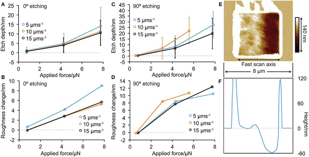
Figure 7. The effect of scan angle and tip speed making five etching passes on 5 μm × 5 μm areas on gold with a diamond-coated probe. (A,B) Etch depth and roughness change, respectively, when scanning at 0°. The slowest speed produces the deepest, roughest trenches. (C,D) Etch depth and roughness change, respectively, when scanning at 90°. The 90° processes produce the deeper trenches with a relatively lower roughness. The middle scan speed produces the deepest, roughest, trenches. We note the large error bars in (A,C), illustrating the large trench roughnesses. (E) Topography of the roughest trench, when etching at 90° and 15 μms−1 with 8 μN applied, demonstrating a deep depression perpendicular to the fast scan axis. (F) Step profile across (E), demonstrating that the deepest part of the trench is over 50 nm below the surface, whilst the shallowest part is raised above the surface.
We next looked at the effect of tip speed and the number of etching passes on etch depth and roughness over 2 μm × 2 μm sampling areas. To try and maximize etch depth and minimize roughening, we scanned at 90° with an applied force of around 1.4 μN. The data are shown in Figure 8. We observe that deeper, smoother trenches are produced at lower tip speeds; applying a force below 2 μN might result in a clearer trend here than that observed in Figure 7. This effect increases linearly with the number of passes, similarly to that in Figure 5. We again note the large error bars on the etch depth, particularly at the highest speed, highlighting the roughening effect. As mentioned in the previous section, nanoscale material removal between sliding contacts results from friction. The coefficient of friction between the probe and sample has been observed to decrease as the tip speed is increased (Huang et al., 2011), thus it follows that greater speeds produce shallower trenches. For completeness, we also looked at the probe following these processes (Supplementary Figure 5). The apex was still sharp and clear of debris, with grain detail present. Thus, it appears that the tip speed and large travel distance did not cause significant damage, if any, at the relatively low applied force.
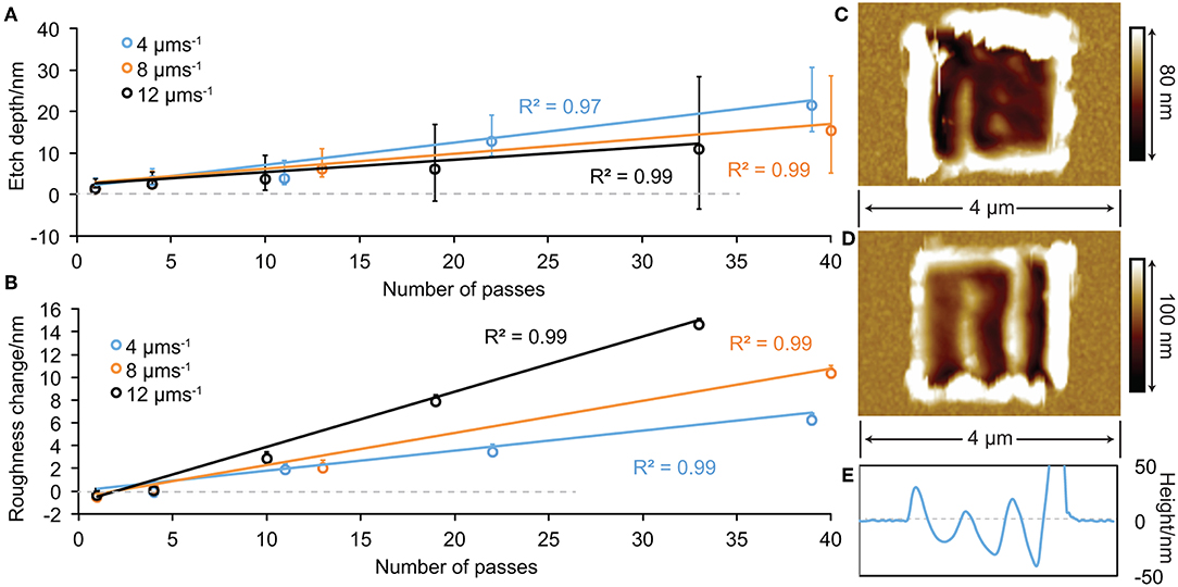
Figure 8. The effect of tip speed and number of passes when etching gold at 1.4 μN with a diamond-coated probe. (A,B) Etch depth and roughness change, respectively. The lowest speed produces the deepest and smoothest trench, though the roughness is always significant in comparison to the depth. (C) Topography of the trench produced for 39 passes at 4 μms−1. There is a distinct wave-like pattern perpendicular to the fast scan axis. (D,E) Topography and step profile, respectively, of the trench produced for 33 passes at 12 μms−1. This was the roughest trench and displays a severe wave-like pattern perpendicular to the fast scan axis.
The roughening of the sample is not small in comparison to the depth at any tip speed or scan angle. This is illustrated well in Figure 8C, where the trench corresponding to 39 passes at 4 μms−1 is shown. There is a clear wave-like pattern perpendicular to the fast scan axis; evidently, the base of the trench is not level and some regions extend tens of nanometers above the surrounding material. However, roughly the same depth is reached for 33 passes at 12 μms−1, which corresponds to the roughest trench produced in this set of processes, as shown in Figures 8D,E. Thus, although etching at 90° with a low tip speed and applied force demonstrates some efficacy in reducing gold roughening, the roughness is always significant relative to the trench depth.
To determine whether instrumental gain affected the gold roughening process, we performed two sets of measurements on 2 μm × 2 μm areas at 1.2 μN, varying the number of etching passes. In one set, we employed typical imaging gain settings as used throughout the work presented here. In the other, we turned the integral and proportional gains to zero, effectively switching off the instrumental feedback. As we see in Figure 9 this results in deeper, smoother trenches than when the feedback is on. We note that the etch depth is always much greater with the feedback off, though it shows a poorer linear fitting; the R2 value when the gain is on is 0.93, compared to 0.56 when the gain is off. This suggests that the etch depth might be even less predictable with the gain off on gold than with the gain on, despite the roughening effect being alleviated. It is not immediately clear why this occurs, because the force applied to the sample should be the same regardless of whether the gain is on or off.
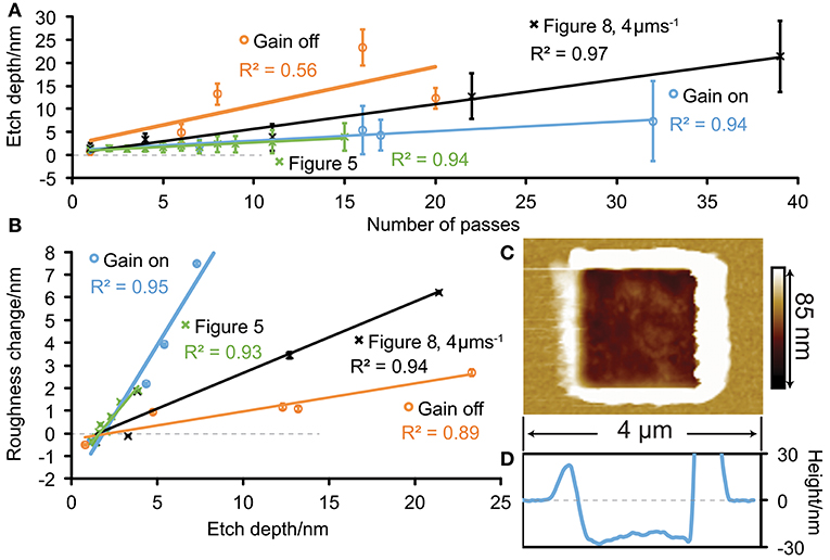
Figure 9. The contrast in gold etching between standard gain settings and turning the gain channels off, compared to previous data presented herein. (A) Etch depth with number of passes, demonstrating a steeper increase in etch depth with number of passes when the gain is off, though with a relatively poor linear fitting. (B) Roughness change with etch depth, demonstrating that switching the gain off significantly reduces the roughening effect. (C,D) Topography and step profile, respectively, of the deepest trench produced with the gain off, for 15 passes. The base is relatively smooth.
We monitored the AFM photodiode voltage (the raw cantilever deflection signal) and noted that the signal for each pass was lower when the gain was off (Supplementary Figure 6); this would correspond to the tip being pressed with greater force into the sample surface. In addition, the signal fluctuated more both within and between passes with the gain off. We surmise that when the deflection setpoint is initially increased to the desired value with the feedback off, the tip is pressed more deeply into surface, as the probe is not retracted to account for the increasing contact force. Following this, the probe scans with little change in height, readily plastically deforming the sample surface and removing material. This ultimately creates a smoother trench, though the depth might be less predictable. Nevertheless, the trench produced is much better suited to tomography.
We also assessed the effect of changes to the process protocol on etching our hard SiOx sample but did not detect a significant effect on either the trench depth or roughness change (Supplementary Figure 7). The lack of variation in etch depth with tip speed is also consistent with other observations (Tseng et al., 2009; Tseng, 2010; Guo et al., 2017). This is thought to be due to invariance in the friction above a threshold speed of around 2 μms−1 (Huang et al., 2012) and is consistent with a plastic material removal process rather than atomic attrition at low applied force (Jacobs and Carpick, 2013). Crucially, the trench is always smoother than its surroundings, suggesting that changes to the scan angle, tip speed or gain would still be appropriate for capturing planar tomography information. Thus, if protocol changes were to be made in order to better etch a softer film, we could expect the same parameters to be suitable for etching neighboring, harder layers.
We suppose that the SiOx is not affected as significantly as the gold by changes in the etching protocol due to its relative hardness and lower adhesion to the diamond probe. The latter was particularly evident when the gain was switched off; the probe periodically lost contact with the surface, so it was necessary to switch the gain on briefly to make contact again (Supplementary Figure 6). The absolute tip height at the chosen deflection setpoint might remain unchanged, such that the shear strength decreases as the surface is worn. Thus, less material would be removed with each consecutive pass. We surmise here that, for both hard and soft samples, the gain might optimally be set low, rather than turned off, in order to ensure surface contact is maintained and shear force induced. We also note that none of the protocol changes appear to have a significant effect on probe wear (Supplementary Figure 7); the appearance of the apices of these probes is similar to those observed elsewhere in this work.
We often encountered one final issue when etching SiOx, namely that a narrow edge region of the sampling volume would be rapidly worn. Typically, this was at one or other bound of the fast scan axis, as shown in Figures 10A,B. This resulted in rapid substrate exposure and thus an undesirable sampling area topography. One approach to this issue is to reduce the scan size, to avoid removing further material from the deep edge, as shown in Figures 10C,D. However, though the measurement may thus progress, either the initial scan area must be larger than the desired size or the final sampling area is reduced. This requires additional instrument time.
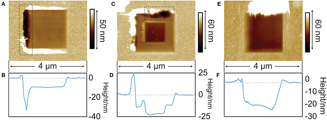
Figure 10. Edging effect, highlighted by dashed boxes, on SiOx when etching with a diamond-coated probe. (A,B) Topography and cross section, respectively, showing the edging effect on a trench. (C,D) Topography and cross section, respectively, showing a trench in which the scan size has been reduced in order to alleviate the edging effect. (E,F) Topography and cross section, respectively, for a trench in which the deflection setpoint was gradually increased to the desired value, eliminating the edging effect.
We looked at whether the edging effect resulted from our experimental protocol, as we would initially position a probe at one edge of the scan area, pause its movement and then increase the deflection setpoint to reach the desired force. Etching would therefore begin from an edge, so we instead tried gradually increasing the deflection setpoint at a rate of around 0.2 V per pass while the probe was in motion, starting from one or other bound of the slow scan axis. As can be seen in Figures 10E,F, this significantly reduces the edging effect, producing a much more consistent trench. Notably, reports have previously been made on such a phenomenon, termed sudden loading (Bourne et al., 2010). Not only is depth inconsistency possible when statically increasing the deflection setpoint to reach the desired force, but there is also a risk of damage to the probe, which would reduce its lifetime. Thus, gradually increasing the force produces a more controlled etch and minimizes probe wear.
General Considerations and Suggestions
We now discuss some final considerations based on our more general observations made during etching measurements, along with a suggested protocol for applying tomography to a new sample material. Here, we hope to provide the reader with a practical foundation for future experimental work, based more directly on our hands-on experience with this technique.
Firstly, one of our aims in this study was to use relatively accessible instrumentation and techniques, in the hope that the results would be generally applicable to other systems. We used only the resonant frequency of the cantilever to estimate its spring constant, as this is a straightforward tapping-mode measurement that should be available on most, if not all, AFM instruments. All measurements were performed in air, as vacuum AFM systems are less common and thus not readily accessible to many research groups. As far as we are aware, there is nothing unique about our microscope and the way in which we operated it is that would prevent our results from being generally applicable; assuming one is able to obtain images of a good quality on their microscope, they should also be able to perform etching measurements without any additional instrumentation (though conductance tomography will of course require a microscope capable of performing conductive AFM).
An important general comment is that our study of full-diamond probes is notably not as thorough as that of diamond-coated probes, so we are unable to comment definitively on which is better suited for etching processes (i.e., produces more consistent, sustained behavior). Furthermore, variations in the fabrication processes between probes, even of the same nominal type (e.g., diamond-coated or full-diamond) cannot be discounted. For example, the grain size and characteristics of any asperities present at the apex might significantly affect the wear rate and etching behavior of a probe. Diamond-coated probes are also typically much less expensive than full-diamond probes, so this is a further accessibility consideration. However, the diamond-coated probes used in this work performed well, giving consistent trends in etching performance and pronounced wear only in the early stages of etching. Thus, we would favor their use in future measurements, until we are able to more thoroughly study the behavior of full-diamond probes.
A further observation is the effect of instrumental drift over the course of long experiments. In this work, each data point (and so each value for depth and roughness) corresponds to a measurement of up to around 1 h. In fact, a single etching pass generally required between 4 and 5 min to complete. However, we have observed lateral drift in previous work and noted that it can have a non-negligible effect on the conductive AFM current mapping and trench geometry (Buckwell et al., 2015a). We note that some interesting work has recently been carried out on accounting for drift by comparing topography images captured at different depths during a conductance tomography measurement (Anderson, 2018). This approach improved the correlation of current mapping with depth, producing a better-aligned conductivity tomogram. In some measurements (not reported here) we have had success with the rather more coarse method of periodically scanning a larger area at an applied force suitable for imaging, then re-aligning the etch with the center of the trench. Of course, this does increase the likelihood of debris adhering to the probe apex.
The above discussion on adjusting the scan area to account for drift extends to an observation on debris accumulation. We note that each data point presented in this work corresponds to a different sample location, suggesting that the trends in etching behavior do not depend strongly on whether the probe maintains contact with the sample or is moved to a new location. However, moving the probe between locations necessarily increases the chance of debris adhering to the apex. Typically, one might suspect debris adherence if significant changes to the topography imaging are observed, such as a pronounced tip artifact (assuming that this is not a result of blunting). In this case, an additional wearing-in or cleaning step might be required in order to restore the etching behavior of the probe. Although we did not find it necessary to clean the probe between any measurements presented herein, in other etching experiments (not reported here) we have found this additional process necessary.
We have not performed a full investigation of our probe cleaning method, but we have noted that using a high contact force to scratch the probe on a ductile material, such as gold, can be effective at removing debris. Typically, we switch off the slow scan axis and scan at 0, 90, and 135° for tens of micrometers travel distance, repeating the process with increasing force until we either note an improvement in the condition of the probe or determine that it is significantly blunted or otherwise rendered unusable. We often need to apply relatively high forces, sometimes tens of micronewtons, though we reason that the risk of further damage to the probe is offset by the possibility of restoring its usefulness. Using this approach we have observed marked improvements in imaging quality (reduction of tip artifacts and an increase in lateral resolution) and electrical properties (greater stability of current-voltage measurements and more consistent current mapping on conductive materials). Thus, we are sometimes able to improve the lifetime of a used probe.
We recognize that the challenge of smoothly etching gold has implications for tomography of ductile materials. We have discussed the improvements observed when the feedback gain is off, but this approach is also limited. As we note, sometimes the probe loses contact with the sample, thus the gain must either be periodically switched on or the scan performed at low gain. Thus, for long measurements on ductile materials, etching with no gain might not be feasible. Furthermore, when the roughening effect is reduced, the etch rate becomes much less predictable. It is reasonable to caution that this etching technique might be inherently limited in its application to ductile materials. However, there are approaches that we have not explored so far. For example, more extreme speed and force combinations might be effective, such as scanning at <1 μms−1 with tens of micronewtons applied, or tens of μms−1 with less than a micronewton applied. We also suppose that alternating between multiple scan angles or using a blunted probe might help smooth out the roughened region. For heterostructures whose ductile layers are not the region of interest (e.g., thick, homogeneous metal contact pads), such methods might be considered pre-treatment steps, wherein the material is thinned, rather than removed. Subsequently, the scan parameters or probe could be changed to remove the remaining material and progress into the layer of interest.
A further consideration for material removal is the combination of conductance tomography with other methods. For example, ion milling or wet etching might be better suited than AFM to removing some materials. Thus, an effective approach to some measurements, particularly for very thick or hard to etch materials, might be to perform a pre-treatment with another technique, before using AFM to study the region or layer of interest. This would also reduce the wear of the probe. It should be noted, however, that care must be taken with any alternative etches that the region of interest is not adversely affected and that the sample does not become more difficult to etch with AFM.
It is reasonable to suggest that a new probe might be tempered for use, in order to stabilize its behavior for better prediction of etch depth, particularly for measurements on heterostructures. For example, by etching briefly at or just above the force that will subsequently be used for tomography. This process likely depends on the sample; harder materials should cause more rapid, pronounced wear. Therefore, we finally combine our observations in order to provide a recommended calibration protocol for researchers interested in carrying out tomography; we stress that this is a generic starting point, such as we might use in our own study of a new sample.
Firstly, initial calibration etches might be made on the hardest material to be sampled during tomography. We suggest starting with a single pass of around a micronewton at a few μms−1, in order to minimize wear and maintain shear force. We would recommend scanning at 90° with the feedback gain set suitably for imaging. The etched trench should then be examined in order to determine whether a reasonable depth has been reached (i.e., that some material has been removed, but not so much that the depth resolution of a measurement at this force would be poor). If necessary, the force might be adjusted and the measurement repeated in order to reach an appropriate depth for a single pass; around 1 nm is likely suitable for thin film samples.
With a suitable force selected, a set of etches might be made with an increasing number of passes to determine how rapidly material would be removed over the course of a tomography measurement. Ideally, the depth should depend linearly on the number of passes; this would suggest that no wear is occurring and that the sample material is removed at a consistent rate. If the trend is non-linear then we would suggest repeating these calibration measurements until linearity is achieved, which would indicate that the probe has been worn-in and thus tempered for stable use.
Once the probe has been suitably worn-in, the chosen force should be applied to each material that composes the sample, if applicable. In each case, multiple passes should be performed in order to confirm that sufficient material is removed at the chosen force. Notably, if any material is challenging to etch, then we would recommend firstly reducing the feedback gain and then adjusting the scan speed in order to etch more effectively. If these adjustments are unsuccessful, we would suggest changing the force applied. We note that in the course of these processes it is possible that the probe becomes significantly blunted, particularly if the applied force is increased. As such, multiple probes might be required in order to prepare a full understanding of the necessary scan parameters for a given sample. Thus, in case only a few probes are available, we highlight that it would be a reasonable to compromise between carrying out a full calibration and performing a measurement with a fresh probe after only a basic calibration or no calibration at all.
Conclusion
The work we present here contributes to the application of AFM in tomography. Our studies on process consistency and comparisons of etching hard and soft materials provide a better understanding of the practicability of this technique. We have shown that probes produce reasonably consistent results with repeated use, although there is a wearing-in process that must be accounted for. Correspondingly, the diamond coating grains of probe apices are observably worn by etching, in particular on the harder sample, for which the wear is concentrated to the wearing-in process. We suppose, also, that continued, more gradual wear occurs.
Importantly, we have not studied here the effect of probe wear on the acquisition of other AFM data types, such as current when operating in conductive mode. Although an increasingly stable apex might be desirable for material removal, gradual changes in its shape and size would surely have a significant impact on other tip-sample interactions, such as the electrical contact area.
Etching processes are consistent between different probes of the same type, demonstrating that there is some predictability to the method. This was particularly true of our SiOx sample. However, our softer gold sample yielded less predictable results at higher applied forces. We suggest initial calibration processes on sample materials would provide insight into achieving a desirable tomography protocol. The greater stability and predictability of etching harder material is encouraging in applying AFM tomography to electronic devices; addressing the issues of etching through softer material should not have a significant impact on neighboring harder layers. Finally, it is important to highlight that there remains an intrinsic variability in processing, even following consideration of the above precautions. Investigation of the applicability of this method to a diversity of sample types is required in order to determine the limits of its reliability.
Data Availability
The datasets generated for this study are available on request to the corresponding author.
Author Contributions
MB designed the study, performed the experimental work, interpreted the data, and wrote the manuscript. WN and AM fabricated the samples. SH assisted with experimental work and data interpretation. ML assisted with study design and writing of the manuscript. AK oversaw the work and assisted with writing of the manuscript.
Funding
This work was supported by the Engineering and Physical Sciences Research Council, UK (grant no. EP/K01739X/1) Leverhulme Trust (grant no. RPG-2016-135), The Worshipful Company of Scientific Instrument Makers, the Young 1000 Global Talent Recruitment Program of the Ministry of Education of China, the National Natural Science Foundation of China (grant nos. 61502326, 41550110223, 11661131002), the Jiangsu Government (grant no. BK20150343), and the Ministry of Finance of China (grant no. SX21400213).
Conflict of Interest Statement
The authors declare that the research was conducted in the absence of any commercial or financial relationships that could be construed as a potential conflict of interest.
Acknowledgments
We also acknowledge The Collaborative Innovation Center of Suzhou Nano Science and Technology, the Jiangsu Key Laboratory for Carbon-Based Functional Materials and Devices, the Priority Academic Program Development of Jiangsu Higher Education Institutions and the 111 Project from the State Administration of Foreign Experts Affairs.
Supplementary Material
The Supplementary Material for this article can be found online at: https://www.frontiersin.org/articles/10.3389/fmats.2019.00203/full#supplementary-material
References
Aghababaei, R., Warner, D. H., and Molinari, J. F. (2016). Critical length scale controls adhesive wear mechanisms. Nat. Commun. 7, 1–8. doi: 10.1038/ncomms11816
Anderson, J. P. (2018). An Alignment Scheme for Atomic Force Tomograms of Conductive Filaments in Resistance Switching Devices. Undergraduate Research Scholars Program. Available online at: http://hdl.handle.net/1969.1/166536 (accessed July 11, 2019).
Arda Gozen, B., and Burak Ozdoganlar, O. (2014). Wear of ultrananocrystalline diamond AFM tips during mechanical nanomanufacturing by nanomilling. Wear 317, 39–55. doi: 10.1016/j.wear.2014.04.024
Bhushan, B., and Marti, O. (2017). “Scanning probe microscopy—principle of operation, instrumentation, and probes,” in Nanotribology and Nanomechanics: An Introduction, 4th Edn., ed B. Bhushan (Cham: Springer), 21–25.
Bourne, K., Kapoor, S. G., and DeVor, R. E. (2010). Study of a high performance AFM probe-based microscribing process. J. Manuf. Sci. Eng. 132:030906. doi: 10.1115/1.4001414
Bousoulas, P., Giannopoulos, J., Giannakopoulos, K., Dimitrakis, P., and Tsoukalas, D. (2015). Memory programming of TiO2–x films by conductive atomic force microscopy evidencing filamentary resistive switching. Appl. Surf. Sci. 332, 55–61. doi: 10.1016/j.apsusc.2015.01.133
Brivio, S., Tallarida, G., Cianci, E., and Spiga, S. (2014). Formation and disruption of conductive filaments in a HfO2/TiN structure. Nanotechnology 25:385705. doi: 10.1088/0957-4484/25/38/385705
Bruker Nano Surfaces (2018). Application Note # 128 Quantitative Mechanical Property Mapping at the Nanoscale with PeakForce QNM. Available online at: http://nanoscaleworld.bruker-axs.com/nanoscaleworld/media/p/418.aspx (accessed June 9, 2018).
Buckwell, M., Montesi, L., Hudziak, S., Mehonic, A., and Kenyon, A. J. (2015a). Conductance tomography of conductive filaments in intrinsic silicon-rich silica RRAM. Nanoscale 7, 18030–18035. doi: 10.1039/C5NR04982B
Buckwell, M., Montesi, L., Mehonic, A., Reza, O., Garnett, L., Munde, M., et al. (2015b). Microscopic and spectroscopic analysis of the nature of conductivity changes during resistive switching in silicon-rich silicon oxide. Phys. Status Solidi 12, 211–217. doi: 10.1002/pssc.201400160
Buckwell, M., Zarudnyi, K., Montesi, L., Ng, W. H., Hudziak, S., Mehonic, A., et al. (2016). Conductive AFM topography of intrinsic conductivity variations in silica based dielectrics for memory applications. ECS Trans. 75, 3–9. doi: 10.1149/07505.0003ecst
Buijnsters, J. G., Tsigkourakos, M., Hantschel, T., Gomes, F. O., Nuytten, T., Favia, P., et al. (2016). Effect of boron doping on the wear behavior of the growth and nucleation surfaces of micro- and nanocrystalline diamond films. ACS Appl. Mater. Interfaces 8, 26381–26391. doi: 10.1021/acsami.6b08083
Celano, U., Goux, L., Belmonte, A., Opsomer, K., Franquet, A., Schulze, A., et al. (2014). Three-dimensional observation of the conductive filament in nanoscaled resistive memory devices. Nano Lett. 14, 2401–2406. doi: 10.1021/nl500049g
Celano, U., Hsia, F.-C., Vanhaeren, D., Paredis, K., Nordling, T. E. M., Buijnsters, J. G., et al. (2018). Mesoscopic physical removal of material using sliding nano-diamond contacts. Sci. Rep. 8:2994. doi: 10.1038/s41598-018-21171-w
Celano, U., and Vandervorst, W. (2017). “Nanoscale three dimensional characterization with scalpel SPM,” in Conductive Atomic Force Microscopy: Applications in Nanomaterials, ed M. Lanza (Weinhein: Wiley), 187–210.
Chen, S., Jiang, L., Buckwell, M., Jing, X., Ji, Y., Grustan-Gutierrez, E., et al. (2018). On the limits of scalpel AFM for the 3D electrical characterization of nanomaterials. Adv. Funct. Mater. 28:1802266. doi: 10.1002/adfm.201802266
Duchamp, M., Migunov, V., Tavabi, A., Mehonic, A., Buckwell, M., Munde, M., et al. (2016). Advances in in-situ TEM characterization of silicon oxide resistive switching memories. Resol. Discov. 1, 27–33. doi: 10.1556/2051.2016.00036
Fang, F. Z., Zhang, X. D., Gao, W., Guo, Y. B., Byrne, G., and Hansen, H. N. (2017). Nanomanufacturing—perspective and applications. CIRP Ann. Manuf. Technol. 66, 683–705. doi: 10.1016/j.cirp.2017.05.004
Fang, T.-H., Weng, C.-I., and Chang, J.-G. (2000). Machining characterization of the nano-lithography process using atomic force microscopy. Nanotechnology 11, 181–187. doi: 10.1088/0957-4484/11/3/308
Fang, T. H., Chang, W. J., and Weng, C. I. (2006). Nanoindentation and nanomachining characteristics of gold and platinum thin films. Mater. Sci. Eng. A 430, 332–340. doi: 10.1016/j.msea.2006.05.106
Garcia, R., Knoll, A. W., and Riedo, E. (2014). Advanced scanning probe lithography. Nat. Nanotechnol. 9, 577–587. doi: 10.1038/nnano.2014.157
García, R., and Perez, R. (2002). Dynamic atomic force microscopy methods. Surf. Sci. Rep. 47, 197–301. doi: 10.1016/S0167-5729(02)00077-8
Geng, Y. Q., Yan, Y. D., Zhao, X. S., Hu, Z. J., Liang, Y. C., Sun, T., et al. (2013). Fabrication of millimeter scale nanochannels using the AFM tip-based nanomachining method. Appl. Surf. Sci. 266, 386–394. doi: 10.1016/j.apsusc.2012.12.041
Gerber, C., and Lang, H. P. (2006). How the doors to the nanoworld were opened. Nat. Nanotechnol. 1, 3–5. doi: 10.1038/nnano.2006.70
Guo, Z., Tian, Y., Liu, X., Wang, F., Zhou, C., and Zhang, D. (2017). Experimental investigation of the tip based micro/nano machining. Appl. Surf. Sci. 426, 406–417. doi: 10.1016/j.apsusc.2017.07.181
Hammock, S. M. (2017). 3D c-AFM Imaging of Conductive Filaments in HfO2 Resistive Switching Devices. Undergraduate Research Scholars Program. Available online at: http://hdl.handle.net/1969.1/164580 (accessed June 26, 2019).
Huang, J.-C., Li, C.-L., and Lee, J.-W. (2012). The study of nanoscratch and nanomachining on hard multilayer thin films using atomic force microscope. Scanning 34, 51–59. doi: 10.1002/sca.20280
Huang, J. C., Lee, J. W., and Li, C. L. (2011). Nano-scratching and nano-machining in different environments on Cr2N/Cu multilayer thin films. Thin Solid Films 519, 4992–4996. doi: 10.1016/j.tsf.2011.01.067
Hui, F., and Lanza, M. (2019). Scanning probe microscopy for advanced nanoelectronics. Nat. Electron. 2, 221–229. doi: 10.1038/s41928-019-0264-8
Jacobs, T. D., and Carpick, R. W. (2013). Nanoscale wear as a stress-assisted chemical reaction. Nat. Nanotechnol. 8, 108–112. doi: 10.1038/nnano.2012.255
Kamaludin, M. S., Thompson, R. J., Hudziak, S., Mitrofanov, O., and Curson, N. J. (2018). Local anodic oxidation lithography on organic semiconductor crystals: oxide depth revealed by conductance tomography. Org. Electron. 63, 231–236. doi: 10.1016/j.orgel.2018.09.041
Kawasegi, N., Takano, N., Oka, D., Morita, N., Yamada, S., Kanda, K., et al. (2006). Nanomachining of silicon surface using atomic force microscope with diamond tip. J. Manuf. Sci. Eng. 128, 723–729. doi: 10.1115/1.2163364
Khurshudov, A. G., Kato, K., and Koide, H. (1996). Nano-wear of the diamond AFM probing tip under scratching of silicon, studied by AFM. Tribol. Lett. 2, 345–354. doi: 10.1007/BF00156907
Landman, U., Luedtke, W. D., Burnham, N. A., and Colton, R. J. (1990). Atomistic mechanisms and dynamics of adhesion, nanoindentation, and fracture. Science 248, 454–461. doi: 10.1126/science.248.4954.454
Lanza, M. (2014). A review on resistive switching in high-k dielectrics: a nanoscale point of view using conductive atomic force microscope. Material 7, 2155–2182. doi: 10.3390/ma7032155
Lanza, M., Celano, U., and Miao, F. (2017). Nanoscale characterization of resistive switching using advanced conductive atomic force microscopy based setups. J. Electroceramics 39, 94–108. doi: 10.1007/s10832-017-0082-1
Lanza, M., Reguant, M., Zou, G., Lv, P., Li, H., Chin, R., et al. (2014). High-performance piezoelectric nanogenerators using two-dimensional flexible top electrodes. Adv. Mater. Interfaces 1:1300101. doi: 10.1002/admi.201300101
Lanza, M., Zhang, K., Porti, M., Nafría, M., Shen, Z. Y., Liu, L. F., et al. (2012). Grain boundaries as preferential sites for resistive switching in the HfO2 resistive random access memory structures. Appl. Phys. Lett. 100:123508. doi: 10.1063/1.3697648
Li, Y., Goyal, A., Chernatynskiy, A., Jayashankar, J. S., Kautzky, M. C., Sinnott, S. B., et al. (2016). Nanoindentation of gold and gold alloys by molecular dynamics simulation. Mater. Sci. Eng. A 651, 346–357. doi: 10.1016/j.msea.2015.10.081
Luria, J., Kutes, Y., Moore, A., Zhang, L., Stach, E. A., and Huey, B. D. (2016). Charge transport in CdTe solar cells revealed by conductive tomographic atomic force microscopy. Nat. Energy 1, 1–6. doi: 10.1038/nenergy.2016.150
Mehonic, A., Buckwell, M., Montesi, L., Munde, M. S., Gao, D., Hudziak, S., et al. (2016). Nanoscale transformations in metastable, amorphous, silicon-rich silica. Adv. Mater. 28, 7549–7549. doi: 10.1002/adma.201670241
Mehonic, A., and Kenyon, A. J. (2016). Emulating the electrical activity of the neuron using a silicon oxide RRAM cell. Front. Neurosci. 10:57. doi: 10.3389/fnins.2016.00057
Mehonic, A., Munde, M. S., Ng, W. H., Buckwell, M., Montesi, L., Bosman, M., et al. (2017). Intrinsic resistance switching in amorphous silicon oxide for high performance SiOx ReRAM devices. Microelectron. Eng. 178, 98–103. doi: 10.1016/j.mee.2017.04.033
Mehonic, A., Shluger, A. L., Gao, D., Valov, I., Miranda, E., Ielmini, D., et al. (2018). Silicon oxide (SiOX): a promising material for resistance switching? Adv. Mater. 30, 1–21. doi: 10.1002/adma.201801187
Merkle, A. P., and Marks, L. D. (2008). Liquid-like tribology of gold studied by in situ TEM. Wear 265, 1864–1869. doi: 10.1016/j.wear.2008.04.032
Mo, Y., Turner, K. T., and Szlufarska, I. (2009). Friction laws at the nanoscale. Nature 457, 1116–1119. doi: 10.1038/nature07748
Moore, P., and Booth, G. (2015). “Failure modes and analysis in metals,” in The Welding Engineer's Guide to Fracture and Fatigue (Cambridge: Woodhead Publishing), 95–110. doi: 10.1533/9781782423911.1.95
Munde, M. S., Mehonic, A., Ng, W. H., Buckwell, M., Montesi, L., Bosman, M., et al. (2017). Intrinsic resistance switching in amorphous silicon suboxides: the role of columnar microstructure. Sci. Rep. 7:9274. doi: 10.1038/s41598-017-09565-8
Ng, W. H., Mehonic, A., Buckwell, M., Montesi, L., and Kenyon, A. (2018). High performance resistance switching memory devices using spin-on silicon oxide. IEEE Trans. Nanotechnol. 17, 884–888. doi: 10.1109/TNANO.2017.2789019
Ogino, T., Nishimura, S., and Shirakashi, J. I. (2008). Scratch nanolithography on Si surface using scanning probe microscopy: influence of scanning parameters on groove size. Jpn. J. Appl. Phys. 47, 712–714. doi: 10.1143/JJAP.47.712
Ohler, B. (2007). Practical Advice on the Determination of Cantilever Spring Constants. Available online at: http://nanoscaleworld.bruker-axs.com/ (accessed June 9, 2018).
O'Shea, S. J., Atta, R. M., Murrell, M. P., and Welland, M. E. (1995). Conducting atomic force microscopy study of silicon dioxide breakdown. J. Vac. Sci. Technol. B Microelectron. Nanom. Struct. 13:1945. doi: 10.1116/1.588113
Palacio, M. L. B., and Bhushan, B. (2010). Normal and lateral force calibration techniques for AFM cantilevers. Crit. Rev. Solid State Mater. Sci. 35, 73–104. doi: 10.1080/10408430903546691
Pan, C., Shi, Y., Hui, F., Grustan-Gutierrez, E., and Lanza, M. (2017). “History and Status of the CAFM,” in Conductive Atomic Force Microscopy: Applications in Nanomaterials, ed M. Lanza (Weinhein: Wiley), 1–28.
Peguiron, A., Moras, G., Walter, M., Uetsuka, H., Pastewka, L., and Moseler, M. (2016). Activation and mechanochemical breaking of C–C bonds initiate wear of diamond (110) surfaces in contact with silica. Carbon 98, 474–483. doi: 10.1016/j.carbon.2015.10.098
Piétrement, O., and Troyon, M. (2001). Study of the interfacial shear strength pressure dependence by modulated lateral force microscopy. Langmuir 17, 6540–6546. doi: 10.1021/la010458u
Pirrotta, O., Larcher, L., Lanza, M., Padovani, A., Porti, M., Nafría, M., et al. (2013). Leakage current through the poly-crystalline HfO2: trap densities at grains and grain boundaries. J. Appl. Phys. 114:134503. doi: 10.1063/1.4823854
Polspoel, W., and Vandervorst, W. (2007). Evaluation of trap creation and charging in thin SiO2 using both SCM and C-AFM. Microelectron. Eng. 84, 495–500. doi: 10.1016/j.mee.2006.10.074
Porti, M., Aguilera, L., Blasco, X., Nafría, M., and Aymerich, X. (2007). Reliability of SiO2 and high-k gate insulators: a nanoscale study with conductive atomic force microscopy. Microelectron. Eng. 84, 501–505. doi: 10.1016/j.mee.2006.10.073
Porti, M., Avidano, M., Nafria, M., Aymerich, X., Carreras, J., and Garrido, B. (2005). Charge storage in Si nanocrystals embedded in SiO2 with enhanced C-AFM. Proc. SPIE 5838, 43–51. doi: 10.1117/12.608206
Pradeep, N., Kim, D. I., Grobelny, J., Hawa, T., Henz, B., and Zachariah, M. R. (2007). Ductility at the nanoscale: deformation and fracture of adhesive contacts using atomic force microscopy. Appl. Phys. Lett. 91, 1–3. doi: 10.1063/1.2815648
Ren, J., Dong, Z., Zhao, J., and Liu, P. (2016). A novel approach for determining the minimum feed in nanochannels processing via molecular dynamics simulation. Appl. Surf. Sci. 369, 584–594. doi: 10.1016/j.apsusc.2016.02.024
Rolandi, M., Quate, C. F., and Dai, H. (2002). A new scanning probe lithography scheme with a novel metal resist. Adv. Mater. 14, 191–194. doi: 10.1002/1521-4095(20020205)14:3<191::AID-ADMA191>3.0.CO;2-7
Sarid, D. (1991). “1.8. Lumped systems,” in Scanning Force Microscopy With Applications to Electric, Magnetic, and Atomic Forces (New York, NY: Oxford University Press), 1–18.
Schulze, A., Hantschel, T., Dathe, A., Eyben, P., Ke, X., and Vandervorst, W. (2012). Electrical tomography using atomic force microscopy and its application towards carbon nanotube-based interconnects. Nanotechnology 23:305707. doi: 10.1088/0957-4484/23/30/305707
Stan, G., Mays, E., Yoo, H. J., and King, S. W. (2016). Nanoscale tomographic reconstruction of the subsurface mechanical properties of low-k high-aspect ratio patterns. Nanotechnology 27:485706. doi: 10.1088/0957-4484/27/48/485706
Tennyson, E. M., Gong, C., and Leite, M. S. (2017). Imaging energy harvesting and storage systems at the nanoscale. ACS Energy Lett. 2, 2761–2777. doi: 10.1021/acsenergylett.7b00944
Tseng, A. A. (2010). A comparison study of scratch and wear properties using atomic force microscopy. Appl. Surf. Sci. 256, 4246–4252. doi: 10.1016/j.apsusc.2010.02.010
Tseng, A. A., Shirakashi, J., Nishimura, S., Miyashita, K., and Notargiacomo, A. (2009). Scratching properties of nickel-iron thin film and silicon using atomic force microscopy. J. Appl. Phys. 106:044314. doi: 10.1063/1.3197313
Wang, Z. Q., Jiao, N. D., Tung, S., and Dong, Z. L. (2011). Atomic force microscopy-based repeated machining theory for nanochannels on silicon oxide surfaces. Appl. Surf. Sci. 257, 3627–3631. doi: 10.1016/j.apsusc.2010.11.091
Wang, Z. Q., Tung, S., and Dong, Z. L. (2012). Material removal model for AFM-based nanochannel fabrication. Wear 278–279, 71–76. doi: 10.1016/j.wear.2012.01.005
Xie, X. N., Chung, H. J., Sow, C. H., and Wee, A. T. S. (2006). Nanoscale materials patterning and engineering by atomic force microscopy nanolithography. Mater. Sci. Eng. R Rep. 54, 1–48. doi: 10.1016/j.mser.2006.10.001
Yan, Y., Geng, Y., and Hu, Z. (2015). Recent advances in AFM tip-based nanomechanical machining. Int. J. Mach. Tools Manuf. 99, 1–18. doi: 10.1016/j.ijmachtools.2015.09.004
Yang, J., Mou, J., and Shao, Z. (1994). Molecular resolution atomic force microscopy of soluble proteins in solution. Biochim. Biophys. Acta 1199, 105–114.
Yang, Y., Huang, L., and Shi, Y. (2016). Adhesion suppresses atomic wear in single-asperity sliding. Wear 352–353, 31–41. doi: 10.1016/j.wear.2016.02.002
Keywords: atomic force microscopy, tomography, etching, lithography, machining, scratching, wear, electronic devices
Citation: Buckwell M, Ng WH, Hudziak S, Mehonic A, Lanza M and Kenyon AJ (2019) Improving the Consistency of Nanoscale Etching for Atomic Force Microscopy Tomography Applications. Front. Mater. 6:203. doi: 10.3389/fmats.2019.00203
Received: 26 March 2019; Accepted: 06 August 2019;
Published: 22 August 2019.
Edited by:
Federico Bosia, University of Turin, ItalyReviewed by:
Hugo Bender, Interuniversity Microelectronics Centre (IMEC), BelgiumPatrick Jacob Shamberger, Texas A&M University, United States
Copyright © 2019 Buckwell, Ng, Hudziak, Mehonic, Lanza and Kenyon. This is an open-access article distributed under the terms of the Creative Commons Attribution License (CC BY). The use, distribution or reproduction in other forums is permitted, provided the original author(s) and the copyright owner(s) are credited and that the original publication in this journal is cited, in accordance with accepted academic practice. No use, distribution or reproduction is permitted which does not comply with these terms.
*Correspondence: Mark Buckwell, bS5idWNrd2VsbEBlZS51Y2wuYWMudWs=