 B. Claflin
 G. J. Grzybowski2
 M. E. Ware
 S. Zollner
- 1Air Force Research Laboratory, Sensors Directorate, Wright-Patterson Air Force Base, Dayton, OH, United States
- 2KBR, Dayton, OH, United States
- 3Department of Electrical Engineering, University of Arkansas, Fayetteville, AR, United States
- 4Department of Physics, New Mexico State University, Las Cruces, NM, United States
A remote plasma enhanced chemical vapor deposition (CVD) process using GeH4, SiH4, and SnCl4 precursors has been developed for epitaxial growth of group-IV alloys directly on Si (100) substrates, without the need for buffer layers. X-ray diffraction measurements of a representative Ge1–xSnx sample which is 233 nm thick, with x = 9.6% show it to be highly oriented along the [001] direction and nearly relaxed, with 0.37% compressive strain. Ellipsometry measurements provide a pseudo-dielectric function which is well fitted by a 3-layer (substrate/alloy/surface oxide) model. Cross-sectional transmission-electron-microscope images show a highly defective interface layer, ∼ 60 nm thick, containing edge dislocations and stacking faults; above this layer, the lattice is well-ordered, with a much lower density of defects. Atomic force microscopy measurements show an RMS roughness of 1.2 nm for this film.
Introduction
Semiconductor devices based on the group-IV elements Si and Ge, as well as their alloys, have dominated many applications in the electronics industry, such as microprocessors for logic circuits, cell phones, global positioning systems (GPS), and wireless communications (WiFi). However, similar progress in optical and electro-optical devices has been limited by the indirect nature of the fundamental energy gap in these materials. In contrast, cubic α-Sn is a zero bandgap, group-IV semiconductor which, when combined in sufficient concentration with Ge, results in a Ge1–xSnx alloy with a direct bandgap (Mathews et al., 2010; Moontragoon et al., 2012; Gupta et al., 2013; Tonkikh et al., 2013; Zaima et al., 2015; Fernando et al., 2018). These Ge1–xSnx alloys have attracted attention as potential low-cost detectors (Chang et al., 2016; Maczko et al., 2016; Tsai and Chang, 2017) and emitters (Wirths et al., 2015; Zhou et al., 2016; Margetis et al., 2018) in the short- and mid-wave-infrared (SWIR and MWIR) spectral regions and can be incorporated into a variety of components (Sun et al., 2007; Soref, 2014; Wirths et al., 2016) for Si-based integrated photonics. Further alloying Ge1–xSnx with Si produces a ternary alloy, Ge1–x–ySiySnx, which allows independent control of lattice constant and bandgap energy (Kouvetakis et al., 2006, 2008).
One significant challenge in the synthesis of Sn-containing group-IV alloys is that the solubility of Sn is ∼ 1% in Ge (Olesinski and Abbaschian, 1984a) and ∼ 0.1% in Si (Olesinski and Abbaschian, 1984b). As a result of these limitations, low temperature, non-equilibrium growth methods are required to deposit Ge1–xSnx and Ge1–x–ySiySnx alloys. Early attempts to produce Ge1–xSnx films by sputtering (Shah et al., 1987; Ishida et al., 1989; Maruyama and Akagi, 1998) or molecular beam epitaxy (Asom et al., 1989; Höchst et al., 1989; Pukite et al., 1989; Piao, 1990; Fitzgerald et al., 1991; Rojas-López et al., 1998; Bratland et al., 2005; Kasper et al., 2012; Oehme et al., 2013) showed limited success, with growth on different substrates (Ge, GaAs) to minimize the lattice mismatch. Many of these samples were amorphous or the crystalline quality was not very high, and film growth was susceptible to Sn segregation.
A major advance in Sn-containing group-IV alloy synthesis was the development of a chemical vapor deposition (CVD) process (Taraci et al., 2001; Bauer et al., 2002, 2003) using SnD4 as the Sn precursor. High quality samples were prepared and characterized, and photoluminescence (PL) was demonstrated for the first time (Soref et al., 2007; Mathews et al., 2010). Higher order germanes and silanes have subsequently been used to increase the reactivity of the precursors, allowing growth at lower temperatures (Beeler et al., 2012; Grzybowski et al., 2012a, b). However, the lack of a commercial supplier for SnD4 and its limited thermal stability led to the identification of SnCl4, a liquid with a reasonably high vapor pressure, as an alternate (Vincent et al., 2011) CVD Sn precursor.
Reduced pressure CVD using SnCl4 has become the preferred method of Ge1–xSnx growth and has attracted interest in these alloys. High quality Ge1–xSnx films with Sn concentrations as high as x = 0.3 have been reported (Wirths et al., 2014; Aubin and Hartmann, 2018; Imbrenda et al., 2018; Zheng et al., 2018; Xu et al., 2019) and optically pumped lasers have been demonstrated (Wirths et al., 2015; Al-Kabi et al., 2016; Stange et al., 2016; Reboud et al., 2017; Margetis et al., 2018; Chrétien et al., 2019; Zhou et al., 2019) at temperatures up to 273 K. Still, this reduced pressure CVD process requires a very high precursor partial pressure ratio (Wirths et al., 2016), PGe2H6/PSnCl4 > 100, to achieve substitutional Sn incorporation with a high degree of crystallinity. In addition, this approach typically requires growth of one or more buffer layers (Ge and/or Ge1–xSnx), sometimes referred to as a virtual substrate, especially for samples with the highest Sn content.
A variation of this method of growth, remote plasma enhanced chemical vapor deposition (RPECVD) (Bàrdoš, 1988), has been used previously to synthesize Si (Lucovsky et al., 1986; Rudder et al., 1986), Ge (Heintze et al., 1990), and Si1–xGex (Kinosky et al., 1991; Qian et al., 1992) films at lower temperatures than those used in conventional CVD processes. In the RPECVD process, an inert gas, typically He or Ar, is excited using an inductively coupled plasma source, and the plasma excited species subsequently interacts with precursor gases introduced downstream, activating them for growth on the substrate. This alternative process for precursor activation allows for thin-film deposition of group-IV alloys at reduced substrate temperatures.
This work describes a process for synthesizing Sn-containing group-IV alloys, directly on Si substrates, using RPECVD to activate GeH4, SiH4 and SnCl4 precursors. The physical, structural, and optical characteristics of a representative Ge1–xSnx sample grown using this RPECVD process are also presented. A more detailed study of the properties of Sn-containing group-IV alloys grown by RPECVD as a function of composition will be reported separately (Grzybowski et al., unpublished).
Experiment
Epitaxy of group-IV alloys containing Sn, grown directly on 2-inch Si substrates, without buffer layers, has been performed via an RPECVD process in a custom designed, ultra-high-vacuum (UHV) chamber using a top-mounted Advanced Energy Litmas RPS 3001 inductively coupled remote plasma tube, as shown schematically in Figure 1. Equipment details for this RPECVD reactor will be published separately (Grzybowski et al., unpublished). Growths of Sn-containing group-IV alloy films have been demonstrated over a range of substrate temperatures, from 295 to 340°C as measured by a thermocouple, and chamber pressures, from 200 to 800 mTorr. X-ray photoelectron spectroscopy (XPS) measurements using a PHI 5500 ESCA system were used to confirm the growth of different Sn-containing alloys. The Si substrates receive a dilute (2.5%) HF:H2O dip to remove their native surface oxide prior to loading into the growth chamber and are heated to the deposition temperature in flowing He prior to flowing precursor gases and initiating the remote plasma.
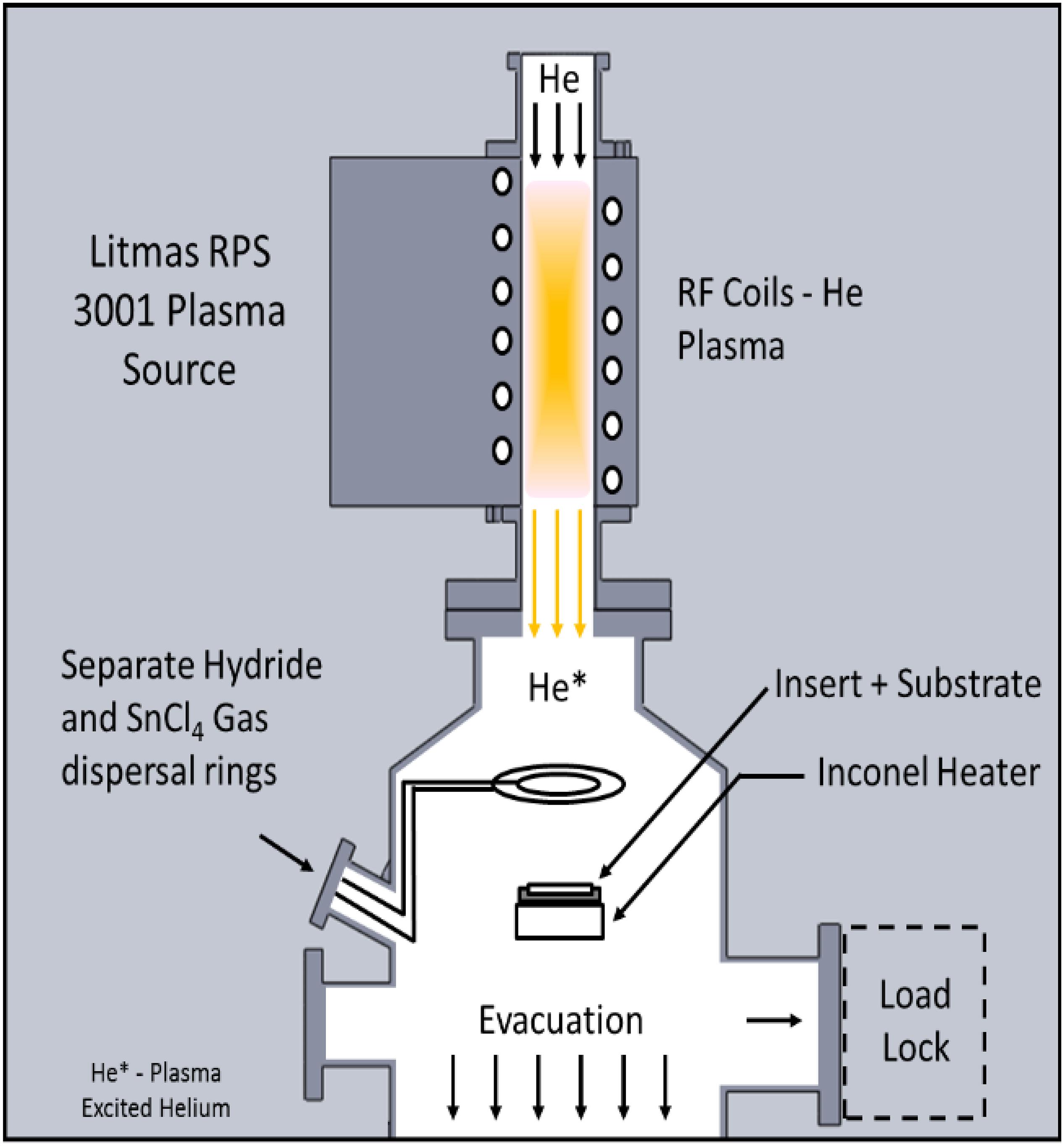
Figure 1. Equipment configuration of RPECVD growth chamber.
For a representative Ge1–xSnx film growth on a 2-inch, p-type, Si (100) substrate, a flow of He gas at 50 SCCM was injected upstream of the RF coil and excited with 1 kW of plasma power. A 50 SCCM flow of 2% GeH4 diluted in He was introduced through a gas dispersal ring, downstream from the plasma as shown in Figure 1. Similarly, a 12.5 SCCM flow of He carrier gas was used to entrain liquid SnCl4 vapor through a bubbler, resulting in a ∼ 2% concentration which was injected through a separate gas injector ring, downstream of the He plasma. A substrate temperature of 325°C and a chamber pressure of 535 mTorr were maintained throughout this film growth.
Film thickness and uniformity of this Ge1–xSnx sample were measured by optical interference with a Filmetrics F50 Thin Film Mapper tool. The pseudo-dielectric function of the film was determined at a 70° angle of incidence from 0.6 to 4.7 eV in 0.01 eV steps using a Jobin Yvon Horiba UVISEL phase modulated spectroscopic ellipsometer. The data were fitted in a three-layer (substrate/alloy/surface oxide) model using the WVASE32 software of the J. A. Woolam Company. The optical constants of the alloy were described using a parametric semiconductor model (Fernando et al., 2018). Reciprocal space maps (RSM) of the (4) reflection and 2θ–ω scans of the (004) reflection were performed using a PANanalyical Empyrean X-ray diffractometer. Film composition and strain were determined (McSkimin, 1953; Xu et al., 2017) using these measured values of lattice parameters and the elastic constants for Ge and Sn. Cross-sectional, bright field, transmission-electron-microscopy (TEM) along the <110> direction was used to evaluate the crystalline structure of the layer as well as to investigate the substrate/film interface. Finally, surface roughness of the sample was measured using a Bruker Dimension atomic force microscope (AFM) in tapping-mode.
Results and Discussion
The RPECVD process provides a robust and reproducible method to synthesize group-IV alloys containing Sn over a range of compositions: Ge1–xSnx films have been produced with Sn concentrations as high as 10%, without surface Sn segregation, as well as Ge1–x–ySiySnx and Si1–xSnx layers. Examples of each of these alloys films as measured by XPS are shown in Figure 2. The relative incorporation of each constituent generally reflects the gas flow ratios of the corresponding precursors. Furthermore, RPECVD provides considerable flexibility in process development to optimize specific material properties of interest.
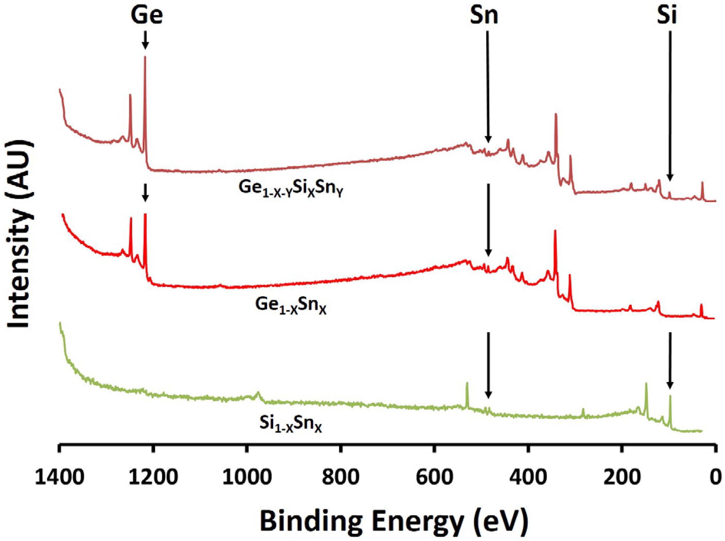
Figure 2. XPS spectra of Ge1–x–ySixSny, Ge1–xSnx, and Si1–xSnx films grown by RPECVD. Peaks corresponding to Ge, Si, and Sn are noted in each spectrum.
A representative example using this RPECVD process is a Ge1–xSnx sample with a thickness of 233 nm, grown at a rate of 2.2 nm/min. Thickness uniformity is typically better than 10% across a 2 inch wafer as a result of the flow dynamics of the reactor, even without the use of sample rotation. It should be noted that without plasma excitation, there is no film deposition under the growth conditions used. Ellipsometry data were well fitted with a 3-layer model (substrate/alloy/surface oxide), as shown in Figure 3, giving an alloy thickness of 217 nm and a surface oxide thickness of 3.9 nm. The oscillations below 2 eV in the pseudo-dielectric function are the result of interference fringes from the film.
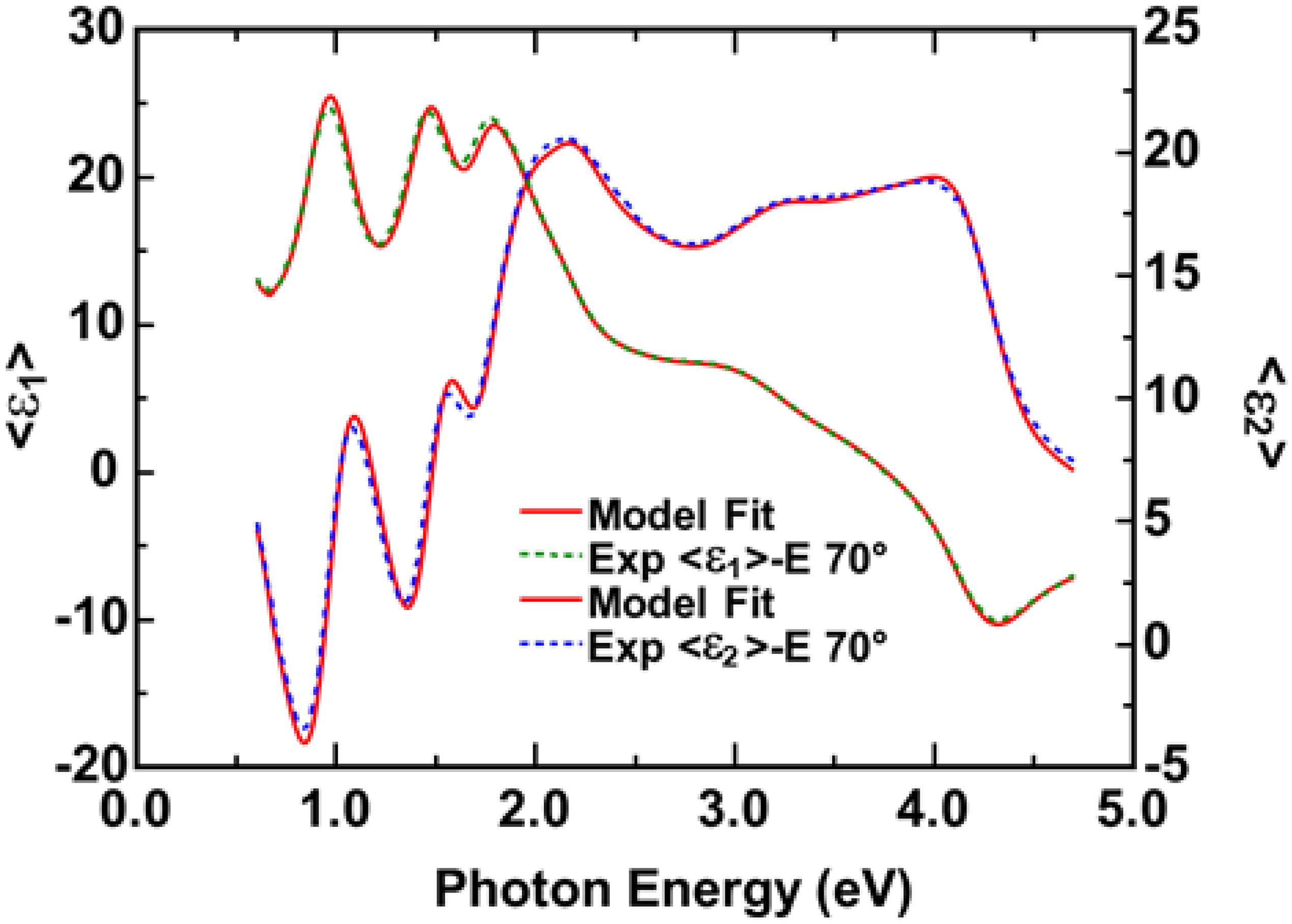
Figure 3. Pseudo-dielectric function of a representative Ge1–xSnx film with x = 9.6% Sn incorporation measured by UV spectroscopic ellipsometry. The solid line shows a 3-layer model fit (substrate/alloy/surface oxide).
An X-ray 2θ–ω scan along [001] superimposed on a corresponding (4) RSM for the representative Ge1–xSnx sample are shown in Figure 4. A (004) Ge1–xSnx peak at 2θ = 64.85° is observed and the RSM shows an asymmetrical (4) reflection that lies close to the relaxation line, indicating that the film is nearly strain relaxed. From the measured lattice constant values, a 9.6% Sn content and 0.37% compressive strain are inferred for this sample. Quantitative values of Sn content derived from X-ray measurements for Ge1–xSnx films grown by RPECVD have been confirmed by Rutherford backscattering (RBS) measurements (not shown) on a number of separate samples.
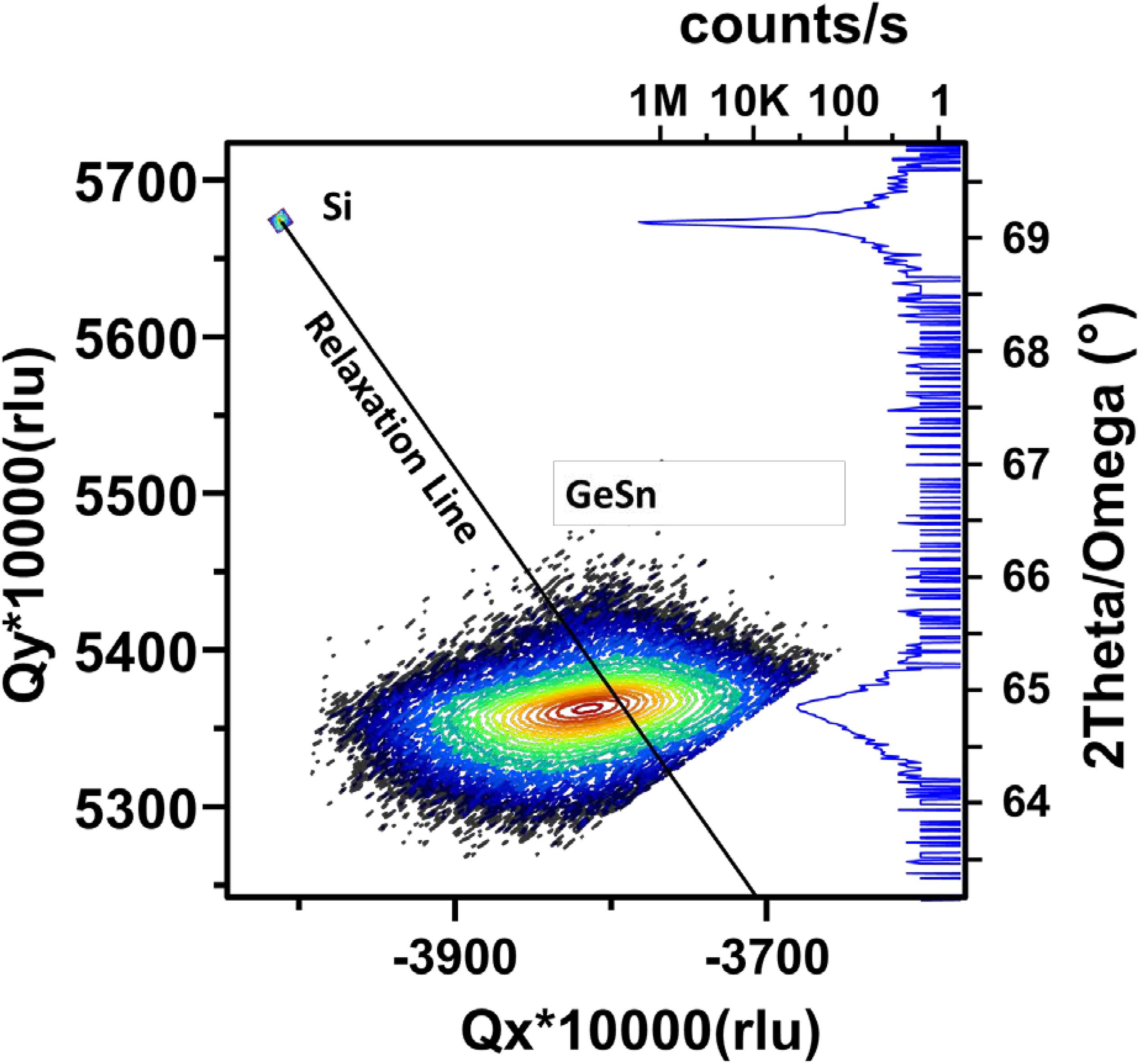
Figure 4. X-ray diffraction 2θ–ω scan along (004) and RSM map around (4) reflection of a representative Ge1–xSnx film grown directly on Si.
A cross-sectional TEM image of the representative Ge1–xSnx alloy is shown in Figure 5. An ∼ 60 nm thick interface layer contains a high density of stacking faults as well as edge dislocations at the substrate interface. Above this interface layer, the crystalline quality of the film improves dramatically and the defect density decreases so that individual threading dislocations can be imaged. The defective interface layer accommodates much of the strain due to the lattice mismatch of Ge1–xSnx and Si, allowing the bulk of the film to relax, consistent with the X-ray results. Most of the stacking faults within this ∼ 60 nm layer appear to annihilate, resulting in the improved crystallinity and lower defect density observed above it. The electrical an optical properties of this interface layer require further investigation since the defects may serve as non-radiative recombination centers or as electrical traps which could impact device applications.
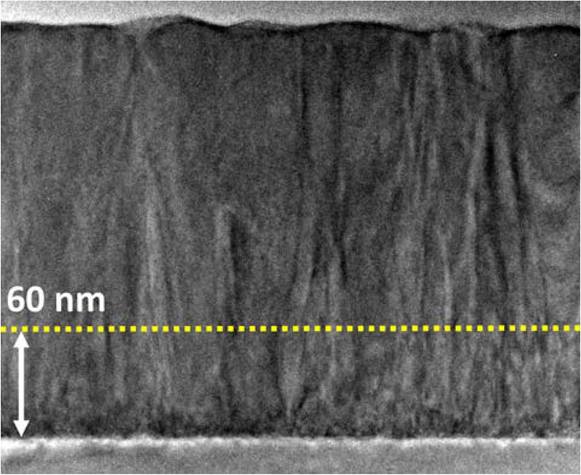
Figure 5. Cross-sectional, bright field, TEM image taken along the <110> direction of a representative Ge1–xSnx film shows a ∼ 60 nm thick interface layer with a high density of stacking faults as well as misfit dislocations at the interface with the substrate. Above this interface layer, the crystalline quality improves dramatically and the defect density is greatly reduced.
Figure 6 shows a 10 μm × 10 μm AFM image of the sample surface. The film is quite smooth, with an RMS roughness of 1.2 nm. There is no indication of the crosshatching which is typically seen in the growth of thick Ge films on Si as a result of strain relaxation from misfit dislocation formation and motion along the Ge/Si interface. This lack of structure on the surface indicates that a different strain relief mechanism dominates in RPECVD alloy films, consistent with the TEM results.
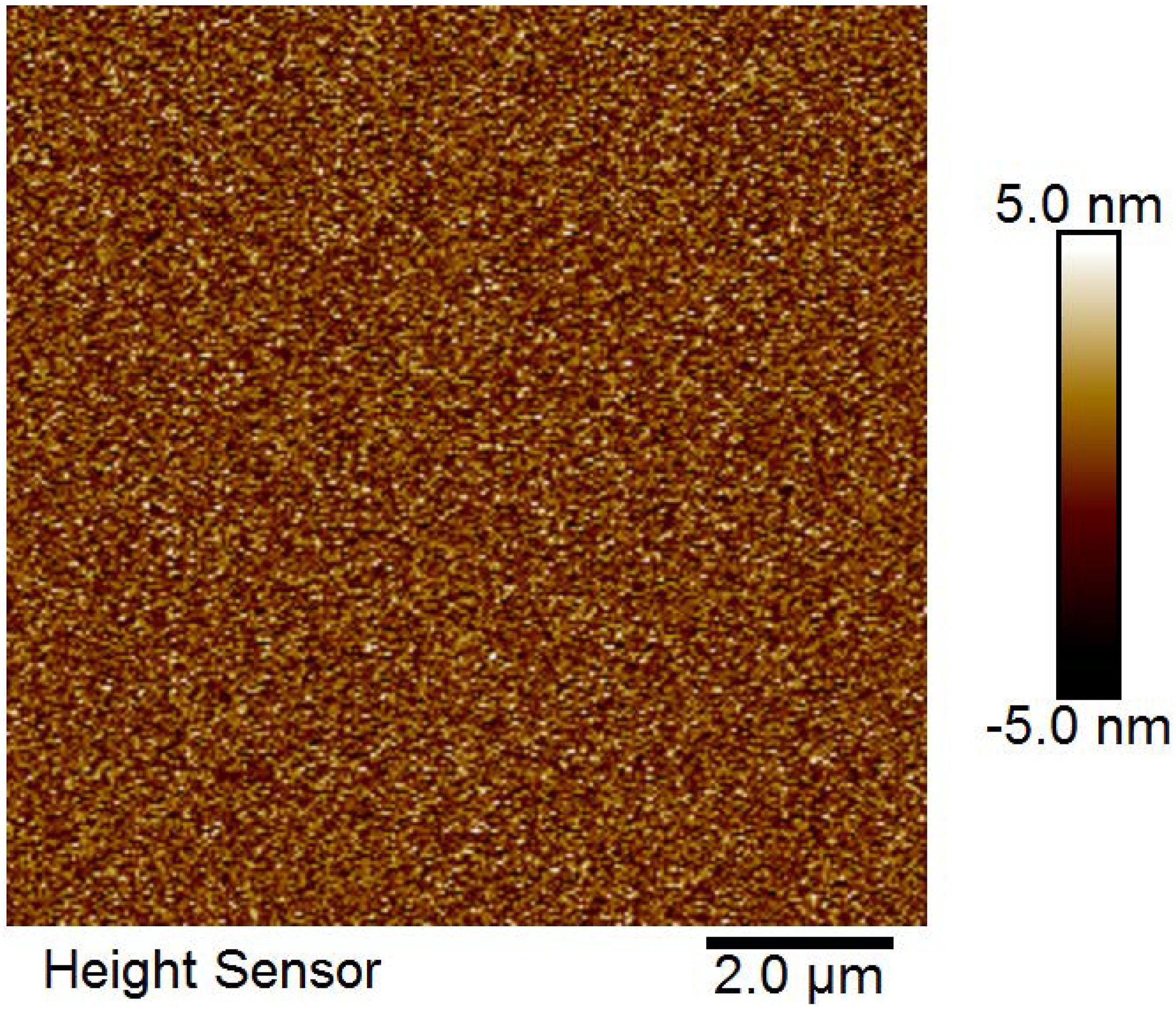
Figure 6. 10 μm × 10 μm AFM image of a representative Ge1–xSnx film shows a smooth surface (1.2 nm RMS roughness). The cross-hatch pattern typically seen for Ge films grown on Si is not observed.
Conclusion
An RPECVD process using GeH4, SiH4, and SnCl4 precursors has been developed for growth of nearly strain relaxed, group-IV alloys containing Sn, directly on Si substrates, without the need for buffer layers. Single crystal alloy films with up to 10% Sn incorporation have been demonstrated without surface segregation of Sn. This remote plasma process uses energy transfer from plasma-excited He to activate the chemical precursors, thereby removing the need for their thermal activation on the substrate surface. This decoupling of the substrate temperature from precursor decomposition allows for independent control of the growth temperature to optimize desired film characteristics. In addition, RPECVD provides a simple process for group-IV alloy growth on Si since buffer layers are not required to produce good structural quality. Finally, the RPECVD process uses a precursor partial pressure ratio that is commensurate with the target film composition, resulting in a much more efficient use of these precursors.
A representative Ge1–xSnx sample synthesized using this RPECVD process has x = 9.6% Sn incorporation and is nearly strain relaxed. Cross-sectional TEM shows a highly defective interface layer ∼ 60 nm thick resulting in a nearly strain relaxed film. The sample surface is very smooth, with an RMS roughness of 1.2 nm as measured by AFM.
Data Availability Statement
The datasets generated for this study are available on request to the corresponding author.
Author Contributions
BC, GG, and AK contributed to conception and design of the study. BC, GG, MW, and SZ provided the analysis and interpretation of data for the work. BC wrote the first draft of manuscript. GG, SZ, MW, and BC made substantial contributions to acquisition, analysis, and interpretation of data for the work. All authors contributed to manuscript revision, read and approved the submitted version.
Funding
This work was supported by AFOSR LRIR 16RYCOR333 and 19RYCOR032 (G. Pomrenke).
Conflict of Interest
The authors declare that the research was conducted in the absence of any commercial or financial relationships that could be construed as a potential conflict of interest.
Acknowledgments
The authors would like to thank Malak Refaei for preparation of the TEM samples and Mourad Benamara for performing the TEM measurements.
References
Al-Kabi, S., Ghetmiri, S., Margetis, J., Pham, T., Zhou, Y., Dou, W., et al. (2016). An optically pumped 2.5?μm GeSn laser on Si operating at 110?K. Appl. Phys. Lett. 109:171105. doi: 10.1063/1.4966141
Asom, M., Fitzgerald, E., Kortan, A., Spear, B., and Kimerling, L. (1989). Epitaxial growth of metastable SnGe alloys. Appl. Phys. Lett. 55:578. doi: 10.1063/1.101838
Aubin, J., and Hartmann, J. (2018). GeSn growth kinetics in reduced pressure chemical vapor deposition from Ge2H6 and SnCl4. J. Cryst. Growth 482:30. doi: 10.1016/j.jcrysgro.2017.10.030
Bàrdoš, L. (1988). Afterglow and decaying plasma CVD systems. Vacuum 38, 637–642. doi: 10.1016/0042-207X(88)90433-2
Bauer, M., Ritter, C., Crozier, P., Ren, J., Menendez, J., Wolf, G., et al. (2003). Synthesis of ternary SiGeSn semiconductors on Si(100) via SnxGe1-x buffer layers. J, Appl. Phys. Lett. 83:2163. doi: 10.1063/1.1606104
Bauer, M., Taraci, J., Tolle, J., Chizmeshya, A., Zollner, S., Smith, D., et al. (2002). Ge–Sn semiconductors for band-gap and lattice engineering. J. Appl. Phys. Lett. 81:2992. doi: 10.1063/1.1515133
Beeler, R., Xu, C., Smith, D., Grzybowski, G., Menéndez, J., and Kouvetakis, J. (2012). Compositional dependence of the absorption edge and dark currents in Ge1-x-ySixSny/Ge(100) photodetectors grown via ultra-low-temperature epitaxy of Ge4H10. Si4H10, and SnD4. Appl. Phys. Lett 101:221111. doi: 10.1063/1.4768217
Bratland, K., Foo, Y., Spila, T., Seo, H.-S., Haasch, R., Desjardins, P., et al. (2005). Sn-mediated Ge / Ge (001) growth by low-temperature molecular-beam epitaxy: surface smoothening and enhanced epitaxial thickness. J. Appl. Phys. 97:044904. doi: 10.1063/1.1848188
Chang, C., Li, H., Ku, C.-T., Yang, S.-G., Cheng, H., Hendrickson, J., et al. (2016). Ge0.975Sn0.025 320 × 256 imager chip for 1.6–1.9 μm infrared vision. Appl. Opt. 55:10170. doi: 10.1364/AO.55.010170
Chrétien, J., Pauc, N., Pilon, F., Bertrand, M., Thai, Q.-M., Casiez, L., et al. (2019). GeSn lasers covering a wide wavelength range thanks to uniaxial tensile strain. ACS Photonics 6, 2462–2469. doi: 10.1021/acsphotonics.9b00712
Fernando, N., Carrasco, R., Hickey, R., Hart, J., Hazbun, R., Schoeche, S., et al. (2018). Band gap and strain engineering of pseudomorphic Ge12x2ySixSny alloys on Ge and GaAs for photonic applications. J. Vac. Sci. Technol. B 36:021202. doi: 10.1116/1.5001948
Fitzgerald, E., Freeland, P., Asom, M., Lowe, W., Macharrie, R., Weir, B., et al. (1991). Epitaxially stabilized GexSnl-x diamond cubic alloys. J. Electron. Mater. 20:489. doi: 10.1007/bf02657831
Grzybowski, G., Beeler, R., Jiang, L., Smith, D., Kouvetakis, J., and Menéndez, J. (2012a). Next generation of Ge1-ySny (y=0.01-0.09) alloys grown on Si(100) via Ge3H8 and SnD4: reaction kinetics and tunable emission. Appl. Phys. Lett. 101:072105. doi: 10.1063/1.4745770
Grzybowski, G., Jiang, L., Beeler, R., Watkins, T., Chizmeshya, A., Xu, C., et al. (2012b). Ultra-low-temperature epitaxy of Ge-based semiconductors and optoelectronic structures on Si(100): introducing higher order germanes (Ge3H8. Ge4H10). Chem. Mater. 24, 1619–1628. doi: 10.1021/cm3002404
Gupta, S., Magyari-Köpe, B., Nishi, Y., and Saraswat, K. (2013). Achieving direct band gap in germanium through integration of Sn alloying and external strain. J. Appl. Phys. 113:073707. doi: 10.1063/1.4792649
Heintze, M., Nebel, C., and Bauer, G. (1990). Deposition of a-Ge:H in a remote plasma ssystem. Mat. Res. Soc. Symp. Proc. 192:565. doi: 10.1557/PROC-192-565
Höchst, H., Engelhardt, M., and Hernandez-Calderon, I. (1989). Angle-resolved photoemission study of thin molecular-beam-epitaxy-grown α-Sn1-xGex films with x 0.5. Phys. Rev. B 40:9703. doi: 10.1103/PhysRevB.40.9703
Imbrenda, D., Hickey, R., Carrasco, R., Fernando, N., VanDerslice, J., Zollner, S., et al. (2018). Infrared dielectric response, index of refraction, and absorption of germanium-tin alloys with tin contents up to 27% deposited by molecular beam epitaxy. Appl. Phys. Lett. 113:122104. doi: 10.1063/1.5040853
Ishida, K., Myoren, H., Yamamoto, M., Imura, T., and Osaka, Y. (1989). Synthesis of metastable GexSn1-x alloys by chemical sputtering in H2. Jap. J. Appl. Phys. 28:L125. doi: 10.1143/JJAP.28.L125
Kasper, E., Werner, J., Oehme, M., Escoubas, S., Burle, N., and Schulze, J. (2012). Growth of silicon based germanium tin alloys. Thin. Solid Films 520:3195. doi: 10.1016/j.tsf.2011.10.114
Kinosky, D., Qian, R., Irby, J., Hsu, T., Anthony, B., Banerjee, S., et al. (1991). Low temperature growth of GexSi1-x/Si heterostructures on Si(100) by remote plasma enhanced chemical vapor deposition. Appl. Phys. Lett. 59:817. doi: 10.1063/1.105272
Kouvetakis, J, D’Costa, V, Fang, Y-Y, Tolle, J, Chizmeshya, A, Xie, J, and Menéndez, J (2008). Independently tunable electronic and structural parameters in ternary Group IV semiconductors for optoelectronic applications. in Proceedings of the Science 5th International Symposium, “Advanced Science and Technology of Silicon Materials” (Kona: The Japan Society for Promotion), 352–356.
Kouvetakis, J., Menendez, J., and Chizmeshya, A. G. V. (2006). Tin-based group IV semiconductors: new platforms for Opto- and microelectronics on silicon. Ann. Rev. Mater. Res. 36, 497–554. doi: 10.1146/annurev.matsci.36.090804.095159
Lucovsky, G., Richard, P., Tsu, D., Un, S., and Markunas, R. (1986). Deposition of silicon dioxide and silicon nitride by remote plasma enhanced chemical vapor deposition. J. Vac. Sci. Technol. A 4, 681. doi: 10.1116/1.573832
Maczko, H., Kudrawiec, R., and Gladysiewicz, M. (2016). Material gain engineering in GeSn/Ge quantum wells integrated with an Si platform. Sci. Rep. 6:34082. doi: 10.1038/srep34082
Margetis, J., Al-Kabi, S., Du, W., Dou, W., Zhou, Y., Pham, T., et al. (2018). Si-Based GeSn lasers with wavelength coverage of 2–3 μm and operating temperatures up to 180 K. ACS Photonics 5, 827. doi: 10.1021/acsphotonics.7b00938
Maruyama, T., and Akagi, H. (1998). Thin films of amorphous germanium-tin alloys prepared by radio-frequency magnetron sputtering. J. Electrochem. Soc. 145:1303. doi: 10.1149/1.1838455
Mathews, J., Beeler, R., Tolle, J., Xu, C., Roucka, R., Kouvetakis, J., et al. (2010). Direct-gap photoluminescence with tunable emission wavelength in Ge1-ySny alloys on silicon. Appl. Phys. Lett. 97:221912. doi: 10.1063/1.3521391
McSkimin, H. (1953). Measurement of elastic constants at low temperatures by means of ultrasonic waves–data for silicon and germanium single crystals, and for fused silica. J. Appl. Phys. 24:988. doi: 10.1063/1.1721448
Moontragoon, P., Soref, R., and Ikonic, Z. (2012). The direct and indirect bandgaps of unstrained SixGe1xySny and their photonic device applications. J. Appl. Phys. 112:073106. doi: 10.1063/1.4757414
Oehme, M., Buca, D., Kostecki, K., Wirths, S., Holländer, B., Kasper, E., et al. (2013). Epitaxial growth of highly compressively strained GeSn alloys up to 12.5% Sn. J. Cryst. Growth 384:71. doi: 10.1016/j.jcrysgro.2013.09.018
Olesinski, R., and Abbaschian, G. (1984a). The Ge-Sn (Germanium-Tin) System. Bull. Alloy Phase Diagr. 5, 265–271. doi: 10.1007/BF02868550
Olesinski, R., and Abbaschian, G. (1984b). The Si-Sn (Silicon-Tin) System. Bull. Alloy Phase Diagr. 5, 273–276. doi: 10.1007/BF02868552
Piao, J. (1990). Molecular-beam epitaxial growth of metastable Ge1-xSnx alloys. J. Vac. Sci. Technol. B 8:221. doi: 10.1116/1.584814
Pukite, P., Harwit, A., and Iyer, S. (1989). Molecular beam epitaxy of metastable, diamond structure SnxGe1-x alloys. Appl. Phys. Lett. 54:2142. doi: 10.1063/1.101152
Qian, R., Kinosky, D., Hsu, T., Irby, J., Mahajan, A., Thomas, S., et al. (1992). Growth of GexSi1-x/Si heteroepitaxial films by remote plasma chemical vapor deposition. J. Vac. Sci. Technol. A 10:1920. doi: 10.1116/1.578116
Reboud, V., Gassenq, A., Pauc, N., Aubin, J., Milord, L., Thai, Q., et al. (2017). Optically pumped GeSn micro-disks with 16% Sn lasing at 3.1 μm up to 180?K. Appl. Phys. Lett. 111:092101. doi: 10.1063/1.5000353
Rojas-López, M., Navarro-Contreras Desjardins, H., Gurdal, O., Taylor, N., Carlsson, J., and Greene, J. (1998). Raman scattering from fully strained Ge 1-x Sn x (x0.22) alloys grown on Ge (001)2×1by low-temperature molecular beam epitaxy. J. Appl. Phys. 84:2219. doi: 10.1063/1.368286
Rudder, R., Fountain, G., and Markunas, R. (1986). Remote plasmaenhanced chemicalvapor deposition of epitaxial Ge films. J. Appl. Phys. 60:3519. doi: 10.1063/1.337604
Shah, S., Greene, J., Abels, L., Yao, Q., and Raccah, P. (1987). Growth of single-crystal metastable Ge1-xSnx Alloys on Ge(100) and GaAs(100) substrates. J. Cryst. Growth 83, 3–10. doi: 10.1016/0022-0248(87)90495-7
Soref, R. (2014). Silicon-based silicon–germanium–tin heterostructure photonics. Phil. Trans. R. Soc. A 372:20130113. doi: 10.1098/rsta.2013.0113
Soref, R., Kouvetakis, J., Menéndez, J., Tolle, J., and D’Costa, V. (2007). Advances in SiGeSn technology. J. Mater. Res. 22, 3281–3291. doi: 10.1557/JMR.2007.0415
Stange, D., Wirths, S., Geiger, R., Schulte-Braucks, C., Marzban, B., von den Driesch, N., et al. (2016). Optically pumped gesn microdisk lasers on Si. ACS Photonics 3:1279. doi: 10.1021/acsphotonics.6b00258
Sun, G., Cheng, H., Menéndez, J., Khurgin, J., and Soref, R. (2007). Strain-free Ge/GeSiSn quantum cascade lasers based on L-valley intersubband transitions. Appl. Phys. Lett. 90:251105. doi: 10.1063/1.2749844
Taraci, J., Zollner, S., McCartney, M., Menendez, J., Santana-Aranda, M., Smith, D., et al. (2001). Synthesis of silicon-based infrared semiconductors in the Ge-Sn system using molecular chemistry methods. J. Am. Chem. Soc. 123, 10980–10987. doi: 10.1021/ja0115058
Tonkikh, A., Eisenschmidt, C., Talalaev, V., Zakharov, N., Schilling, J., Schmidt, G., et al. (2013). Pseudomorphic GeSn/Ge(001) quantum wells: examining indirect band gap bowing. Appl. Phys. Lett. 103:032106. doi: 10.1063/1.4813913
Tsai, C.-H., and Chang, G.-E. (2017). Proceedings of SPIE 10231, GeSn/Ge quantum well photodetectors for short-wave infrared photodetection: experiments and modeling. Optical Sensors 10231:10231J. doi: 10.1117/12.2265185
Vincent, B., Gencarelli, F., Bender, H., Merckling, C., Douhard, B., Petersen, D., et al. (2011). Undoped and in-situ B doped GeSn epitaxial growth on Ge by atmospheric pressure-chemical vapor deposition. Appl. Phys. Lett. 99:152103. doi: 10.1063/1.3645620
Wirths, S., Buca, D., and Mantl, S. (2016). Si–Ge–Sn alloys: from growth to applications. Prog. Cryst. Prog. Cryst. Growth Charact. 62:1. doi: 10.1016/j.pcrysgrow.2015.11.001
Wirths, S., Buca, D., Ikonic, Z., Harrison, P., Tiedemann, A., Holländer, B., et al. (2014). SiGeSn growth studies using reduced pressure chemical vapor deposition towards optoelectronic applications. Thin. Solid Films 557:183. doi: 10.1016/j.tsf.2013.10.078
Wirths, S., Geiger, R., Von Den, Driesch, N., Mussler, G., Stoica, T., et al. (2015). Lasing in direct-bandgap GeSn alloy grown on Si. Nat. Photon. 9:88. doi: 10.1038/NPHOTON.2014.321
Xu, C., Senaratne, C., Culbertson, R., Kouvetakis, J., and Menéndez, J. (2017). Deviations from Vegard’s law in semiconductor thin films measured with X-ray diffraction and Rutherford backscattering: the Ge1-ySny and Ge1-xSix cases. J. Appl. Phys. 12:125702. doi: 10.1063/1.4996306
Xu, C., Wallace, P., Ringwala, D., Chang, S., Poweleit, C., Kouvetakis, J., et al. (2019). Mid-infrared (3–8 μm) Ge1-ySny alloys (0.15 < y < 0.30): synthesis, structural, and optical properties. Appl. Phys. Lett. 114:212104. doi: 10.1063/1.5100275
Zaima, S., Nakatsuka, O., Taoka, N., Kurosawa, M., Takeuchi, W., and Sakashita, M. (2015). Growth and applications of GeSn-related group-IV semiconductor materials. Sci. Technol. Adv. Mater. 16:043502. doi: 10.1088/1468-6996/16/4/043502
Zheng, J., Liu, Z., Zhang, Y., Zuo, Y., Li, C., Xue, C., et al. (2018). Growth of high-Sn content (28%) GeSn alloy films by sputtering epitaxy. J. Cryst. Growth 492:29. doi: 10.1016/j.jcrysgro.2018.04.008
Zhou, Y., Dou, W., Du, W., Ojo, S., Tran, H., Ghetmiri, S., et al. (2019). “Si-based mid-infrared GeSn-Edge-emitting laser with operating temperature up to 260 K,” in Proceedings of the Conference on Lasers and Electro-Optics, OSA Technical Digest, AW3P.3, San Jose, CA, doi: 10.1364/CLEO_AT.2019.AW3P.3
Keywords: RPECVD, characterization, growth process, GeSn and GeSiSn alloys, crystalline
Citation: Claflin B, Grzybowski GJ, Ware ME, Zollner S and Kiefer AM (2020) Process for Growth of Group-IV Alloys Containing Tin by Remote Plasma Enhanced Chemical Vapor Deposition. Front. Mater. 7:44. doi: 10.3389/fmats.2020.00044
Received: 17 December 2019; Accepted: 11 February 2020;
Published: 18 March 2020.
Edited by:
Wei Du, Wilkes University, United StatesReviewed by:
Josep Albero, Instituto de Tecnología Química (ITQ), SpainYun Zheng, Jianghan University, China
Copyright © 2020 Claflin, Grzybowski, Ware, Zollner and Kiefer. This is an open-access article distributed under the terms of the Creative Commons Attribution License (CC BY). The use, distribution or reproduction in other forums is permitted, provided the original author(s) and the copyright owner(s) are credited and that the original publication in this journal is cited, in accordance with accepted academic practice. No use, distribution or reproduction is permitted which does not comply with these terms.
*Correspondence: B. Claflin, YnJ1Y2UuY2xhZmxpbi4xQHVzLmFmLm1pbA==