 Changjiao Ke
 Chunling Tian1*
- 1School of Physical Science and Technology, Southwest University, Chongqing, China
- 2Xi'an Modern Chemistry Research Institute, Xi'an, China
To develop an efficient photocatalyst with intense visible light absorption and high charge mobility is important but still remains a problem. In this work, we have explored the electronic properties of C-monodoped, C-Ge, and C-Sn codoped GaN nanosheets by the hybrid density functional theory in order to find the excellent photocatalytic materials. Results indicate the monodoping of C introduces unoccupied impurity states inside the band gap that serve on recombination centers. Thus, the C monodoping is not suitable to ameliorate visible light absorption. Moreover, the C-Ge and C-Sn codoping not only successfully reduce the band gap of nanosheet GaN but also avoid the unoccupied impurity states. The charge-compensated C-Ge and C-Sn codoped GaN nanosheets are energetically favorable for hydrogen evolution but not insufficient to produce oxygen, indicating that they could serve as Z-scheme photocatalysts. In particular, the minimum defect formation energy of C-Ge is negative and lowest. The C-Ge codoped GaN system has dynamic stability. So, the C-Ge codoped nanosheet GaN is one of the most prospective candidates for the decomposition of hydrogen from water.
1. Introduction
Gallium nitride (GaN) has attracted considerable interest in recent years for its excellent photoelectric properties. With a large band gap (3.04 eV) (Bastos et al., 2018), GaN is widely used as short-wavelength light-emitting diodes (Ha et al., 2007) and room-temperature laser diodes (Feng et al., 2017). The conduction band edge of bulk GaN is at 0.5 eV higher than the redox potential of H+/H2, which implies that the GaN can decompose hydrogen from water (Maeda et al., 2005; Kida et al., 2006). Its wide band gap, however, makes GaN photochemically active only under UV light irradiation. In order to extend the visible light response of GaN, some efforts have been made based on band gap engineering strategies. It was found that Cr-O codoping significantly narrows the band gap of GaN, but this leads to an intermediate band entering the band gap (Pan et al., 2010), which increases the probability of carrier capture. Similar results were obtained for V-O codoped GaN (Meng et al., 2012).
According to the recent theoretical calculations (Freeman et al., 2006), the monolayer GaN has a honeycomb structure similar to that of graphene (Castro Neto et al., 2009), and boron nitride nanosheets (Golberg et al., 2010). These two-dimensional (2D) atomic-layer nanomaterials are interesting topics for their picturesque properties, which would have advantages over bulk structures in many cases (Onen et al., 2016). Particularly, the 2D GaN has a large specific surface area and shorter carrier migration distance etc., and it can remain in high-temperature environments (Sun et al., 2017). The unique properties of nanosheets GaN motivate our research into whether a tunable band gap could be obtained via chemical modification. In this work, the C-monodoping and C-Ge and C-Sn codoping were used to modulate the band structure of GaN nanosheet. We focused our studies on the structure, electronic properties, and minimum defect formation energies of the doped GaN nanosheets.
2. Computational Method
Our first-principles calculations were executed by using density functional theory (DFT) within generalized gradient approximation (GGA) (White and Bird, 1994) parameterized by Perdew, Burke, and Ernzerhof (PBE) (Ernzerhof and Scuseria, 1999), as realized in VASP code (Kresse and Furthmüller, 1996; Kresse and Joubert, 1999). Projector augmented wave (PAW) (Blöchl, 1994) potentials were employed to treat interactions between ions and valance electrons. The electron configuration of N (2s2p3), Ga (3d104s24p1), C (2s22p2), Ge (3d104s24p2), and Sn (5s25p2) were chosen to construct the potential function, respectively. All the calculations were carried out with a plan-wave cutoff energy of 550 eV. We adopted vacuum space of 20 Å along the z-direction in order to wipe out the interaction between the periodic images. All the atomic structure energy convergence tolerance for self-consistent iteration was set to 1.0 × 10⁻⁵ eV, and the convergence criteria force was set to 0.01 eVÅ−1. The Brillouin zone integrations were approximated with a 9 × 9 × 1 k-point (Monkhorst and Pack, 1976) for the GaN nanosheet structure relaxation and electronic properties calculations. The GGA-PBE algorithm will underrate the band gap value of the semiconductor. The accurate electronic structure was calculated by the Heyd-Scuseria-Ernzerhof (HSE06) (Heyd et al., 2003; Heyd and Scuseria, 2004) hybrid functional method. The HSE06 expression for the exchange-correlation energy was written a:
The exchange-correlation energy includes the short- and long-ranged parts. Here, the SR is the short-range parts, and LR stands for the long-ranged. χ represents the mixing coefficient and is set to 0.25. μ indicates the screening parameter and is set to 0.2. In addition, the total density of states (TDOS) and the projected density of states (PDOS) are calculated by the tetrahedral method with Blöchl correction (Blöchl et al., 1994).
3. Results and Discussion
3.1. Pure GaN Nanosheet
The GaN nanosheet is the (001) facet of the optimized bulk, which has a honeycomb graphite structure. This structure is shown in Figures 1A,B. The Ga-N bond length is 1.849 Å and is smaller than in the bulk GaN case (1.966 Å) (Sahin et al., 2009). Since the sp2 bond is stronger than the sp3 bond, the bond length in the GaN nanosheet becomes shorter. The Figure 1C displays the band structure of the GaN nanosheet with the band gap of 3.41 eV using the HSE06 functional. The VBM is located at the k point while the CBM is at the Γ point, which means that the GaN nanosheet is the indirect band gap semiconductor. According to the Figure 1D, the GaN nanosheet has non-magnetic semiconducting character, and the VBM and CBM are predominantly derived from N 2p, Ga 4p, and Ga 3d orbits. The hybridization between the N 2p, Ga 4p, and Ga 3d orbits are located at the bottom of the conduction band. The bond length dGa−N, lattice constant a, and band gaps calculated by the PBE and HSE06 functionals are given in Table 1. Our theoretical data have exhibited good agreement with previous studies (Maruska and Tietjen, 1969; Armstrong et al., 2005; Zeyan et al., 2008; Sahin et al., 2009; Xia et al., 2013; Bastos et al., 2018), which indicates that the calculation methods in this study are reasonable. It can be found that the PBE algorithm will underestimate the band gap of GaN nanosheet. Therefore, the HSE06 algorithm is adopted to study the electronic structures of the GGA-PBE optimized phases.
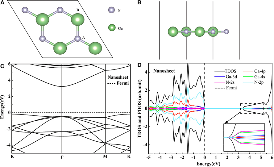
Figure 1. The top (A) and side (B) views of GaN nanosheet. The HSE06 calculated band structure (C) and DOS (D) of the pure GaN nanosheet.
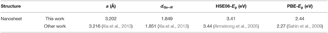
Table 1. The obtained lattice constant a, bond length dGa−N, and band gap Eg with the PBE and HSE06 functional.
3.2. Monodoping in the GaN Nanosheet
In this section, we studied the effect of C doping on the electronic properties of the nanosheet GaN. For GaN1−xCx, the nanosheets (with x = 0.125) were modeled by replacing aneutral N atom (A site in Figure 1A) with a C atom in the 2 × 2 × 1 supercell of the GaN nanosheet. Because the charge number of the doping system is less than that of the pure system, we considered the spin-polarization effect in the calculation.
For the C modoped GaN nanosheet, the bond distance between the C atom and the nearest-neighboring Ga atom is 1.911 Å, which is close to the bond distance (1.849 Å) of Ga-N in nanosheet GaN. The minor difference may be explained by the ionic radius difference between C and N atom. The DOS and band structure of GaN nanosheets with the C doping presented in Figures 2A,B. For both C monodoped systems, the VBM is mainly contributed by mixing of the N 2p, C 2p, Ga 4p, and Ga 3d states, whereas the CBM is primarily contributed by the mixing of the between Ga 4p, N 2p, Ga 3d, and C 2p states. C dopant introduces the unoccupied impurity states on the spin down direction. The impurity state formed by a strong hybrid of C 2p and Ga 4p is very close to the conduction band of GaN. The generation of the impurity state may be due to the fact that the C and N are elements of the same cycle, and the p-orbital energy of C is thus higher than that of N. Electrons in the valence band can easily migrate to the conduction band through these impurity states. Although the band gaps for C doping GaN nanosheet decrease to 1.84 eV, the monodoped system has partially unoccupied impurity states at top of Fermi level. These impurity states can facilitate electron-hole recombination and have destructive influence on the photocatalytic activity. It indicates that C monodoped GaN nanosheet is not suitable for a visible light photocatalyst.
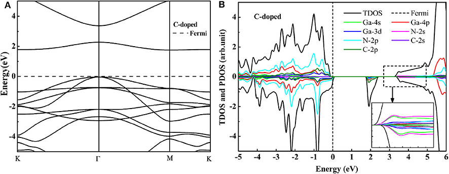
Figure 2. The HSE06 calculated band structure (A) and DOS (B) of the C monodoped GaN nanosheet.
3.3. Codoping in the GaN Nanosheet
To overcome the unoccupied impurity states, the anion-cation passivated codoping was utilized to maintain the charge balance (Gai et al., 2009). In this section, we have discussed the influence of codoping C-Ge and C-Sn on the electronic properties of the supercell 2 × 2 × 1 GaN nanosheet. The C atom substitutes the N atom (A site in Figure 1A), and the Ge (or Sn) atom substitutes the Ga atom (B site in Figure 1A), respectively. For C-Ge and C-Sn codoping, the N-Ge bond length is 1.829 Å, and the N-Sn bond distance is 2.00 Å, decreasing 0.02 Å, and increasing 0.151Å, respectively, with comparison with the N-Ga bond length (1.849 Å). The C-Ge bond length is 1.810 Å and the C-Sn bong length is 1.986 Å. The DOS and band structure for the C-Ge are plotted in Figure 3. According to the DOS, we found that the VBM is dominated by C 2p, Ga 4p, N 2p, and Ga 3d states, whereas the CBM is dominated by N 2s, Ge 4s, Ga 4s, and N 2p states. Since the band structures display that the VBM and CBM are located at the Γ point, the C-Ge system is the direct band gap semiconductor. The calculated band gap of C-Ge codoped GaN nanosheet is 1.83 eV. The DOS of C-Sn doping is plotted in Figure 4B. It indicates that the VBM is dominated by C 2p, Ga 4p, N 2p, and Ga 3d, whereas the CBM is dominated by Sn 5s, N 2p, Ga 4p, and Sn 4d. These configurations have strong hybridization at the top of the valence band and at the bottom the conduction band. According to Figure 4A, the calculated band gap of C-Sn codoped GaN nanosheet is 1.85 eV. The interesting phenomenon is that the impurity states are completely occupied for codoped GaN nanosheets.
Figure 3. The HSE06 calculated band structure (A) and DOS (B) of the C-Ge codoped GaN nanosheet.
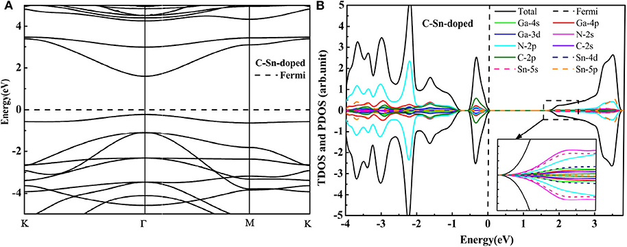
Figure 4. The HSE06 calculated band structure (A) and DOS (B) of the C-Sn codoped GaN nanosheet.
As discussed above, those results indicate that the nanosheet GaN changes from an indirect band gap to a direct band gap by C-Ge and C-Sn codoping. The nanosheet GaN band gap decreases from 3.41 to 1.83 eV in the C-Ge codoping case and to 1.85 eV in the C-Sn codoping one. Smaller band gap values and a direct band gap are beneficial for excited state electronics, as they allow for greater ease with which to jump to the conduction band. At the same time, the smaller band gap value is favorable for moving the absorption spectrum to the visible light region. Therefore, the C-Ge and C-Sn codoped nanosheets GaN are likely to remarkable candidates for visible light photocatalyst.
3.4. Defect Formation Energy
We have calculated the defect formation energy (Ef) for evaluating the stability of doping system in each case. The defect formation energy is defined as (Van de Walle and Neugebauer, 2004; Castleton et al., 2006):
Here, E(doped) and E(GaN) indicate the total energies of doped and pure nanosheet GaN, respectively. ni represents the number of the atoms that has been added to (ni>0) or removed from (ni<0) the pure system for the construction doped nanosheet GaN, while μi is the chemical potential of the element i, and its value μi rests with the synthetic environment
Here, μGaN(nanosheet) represents the chemical potential, which is equal to the energy of the unit cell. As the chemical potential of Ga and N cannot exceed that of the Ga bulk μGa(bulk) and N gas μN(gas), the following rules must be obeyed
To form the nanosheet GaN naturally, the minima of μGa and μN will satisfy
Here, E(GanNn) is the total energy of perfect system with n primitive cells, E(Gan−1Nn) the total energy with Ga defect, and E(GanNn−1) the total energy with N defect. We set the ΔμGa=μGa−μGa(bulk) and ΔμN=μN−μN(gas). In this article, only the minimum defect formation energies of doped GaN nanosheets have been estimated; e.g., the defect formation energy take the minimum value when μGa equals μGa(bulk). The minimum formation energies for doping GaN nanosheets are shown in Figure 5, and the results are outlined in Table 2.
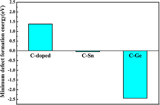
Figure 5. The obtained minimum defect formation energies for monodoped and codoped GaN nanosheets.
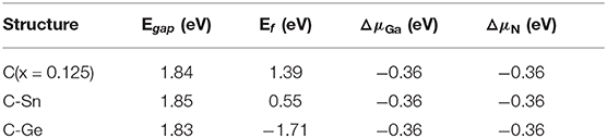
Table 2. The calculated band gaps (Egap), minimum defect formation energies (Ef), and chemical potentials of N and Ga.
From the above discussion, we know that the minimum defect formation energy for the C monodoping is positive, which means that the C monodoping is more difficult to form because the electronegativity of C is less than that of N. The C-Ge and C-Sn codoping minimum defect formation energies are significantly lower than C monodoping. Importantly, the minimum defect formation energy of the C-Ge codoped is negative and lowest, which is greatly reduced by the opposite charge states of C-Ge atoms.
3.5. Band Edge Alignment
It is well-known that an excellent photocatalyst should not only have an appropriate band gap but also suitable band edge positions, i.e., The water reduction level and oxidation level must lie between the CBM and VBM in order to thermodynamically allow for both the hydrogen evolution reaction and oxygen evolution. On the basis of the band edge positions, some photocatalysts are suitable for only hydrogen evolution, and some photocatalysts are good for only oxygen evolution, which is called the Z-scheme photocatalysis system. Here, we have considered the situation of the standard water reduction level (−4.44 eV) and oxidation level (−5.67 eV) with respect to the vacuum level (Chakrapani et al., 2007). A large vacuum space has been used to calculate the absolute position of the band edge for quantitatively comparing with the water redox potentials. As the calculated vacuum level is a relative value, we have shifted the energy value of the CBM (VBM) for each system by subtracting this value to obtain the absolute band edge position.
The calculated positions of the CBM and VBM of the pure and doped GaN nanosheets with respect to the standard hydrogen electrode potentials are indicated in Figure 6. Compared to the band edge potentials of pure GaN, both CB and VB edges of codoped systems are increased. The calculated CBM and VBM of C-Ge (C-Sn) codoped nanosheet are located at −3.50 eV (−3.55 eV) and −5.33 eV (−5.40 eV), respectively. The CBM of C-Ge (C-Sn) is 0.90 eV (0.85 eV) above the water reduction level, and the VBM of C-Ge (C-Sn) is 0.34 eV (0.27 eV) above the water oxidation level. Thus, the C-Sn and C-Ge codoped GaN nanosheets are energetically favorable for hydrogen evolution but not insufficient to produce oxygen, indicating that they could serve as Z-scheme photocatalysts.
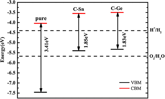
Figure 6. The calculated VBM and CBM positions of pure and codoped GaN nanosheets with respect to the water redox potentials.
3.6. Optical Properties
Optical properties play a critical role in evaluating the performance of photocatalysts in the visible light region. Thus, we have investigated the optical absorption spectra of the pure and codoped GaN nanosheets. The absorption coefficient α(ω) satisfies the following relation (Onen et al., 2016)
where ε1(ω) is the real part that is obtained using the Kramers-Kronig transformation, and ε2(ω) is the imaginary part, which has been calculated by summing over a large amount of empty states. Figure 7 shows the obtained absorption coefficient of pure and codoped GaN nanosheets. It can be seen that the C-Sn and C-Ge codoped can harvest a longer wavelength of visible light spectrum compared to the pure GaN nanosheet for visible light photocatalysis, which can be attributed to the reasonable band gap reduction.
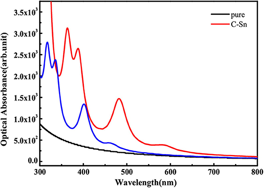
Figure 7. The optical absorption spectra of pure and codoped GaN nanosheets.
3.7. Dynamical Stability
Phonon calculations provide a criterion for the stability of one structure and indicate, through soft modes, structural instability (Ahmad Khandy et al., 2019; Xuan et al., 2019; Ahmad Khandy and Chai, 2020). We therefore calculated phonon dispersion curves for the codoped GaN nanosheet. The C-Ge codoping system was considered, as it has a negative formation energy and can be stably formed. Figure 8 shows the phonon dispersion curves (PDCs) of C-Ge codoping system obtained using GGA scheme, which contains 24 phonon branches composed of Ga3GeN3C cell, including three acoustic modes and 21 optical modes. It is obvious from the figure that there is no virtual frequency in this doping system. It can therefore be concluded that the C-Ge codoped GaN system has dynamic stability.
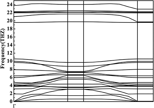
Figure 8. Phonon dispersion for C-Ge codoped GaN nanosheet.
4. Conclusions
The electronic properties of C monodoped, C-Ge, and C-Sn codoped GaN nanosheets have been investigated at the HSE06 level of theory. For C monodoping, the effective band gap values of the GaN1−xCx(x = 0.125) nanosheet can be decreased. However, the C monodoping will introduce the unoccupied impurity states, which leads to the decrease of carrier concentration. The band gap values for the C-Ge and C-Sn codoping GaN nanosheets are 1.83 and 1.85 eV, respectively. Narrow band gap semiconductors can absorb and utilize visible light, and semiconductors can thus be used in solar energy conversion and photocatalysis. The C-Ge and C-Sn codoping GaN nanosheets are direct band gap semiconductors, which make them more advantageous over other materials. Anionic (C) and cationic (Ge or Sn) compensated cooping, greatly reducing the minimum formation energy of doping. However, the minimum defect formation energy of the C-Ge codoping GaN nanosheet is the smallest. The C-Ge and C-Sn codoped systems may be a potential candidate for photocatalytic water splitting to generate hydrogen because of their appropriate band gap and band edge positions. More importantly, the result of the optical absorption spectral analysis shows that the C-Ge and C-Sn codoped GaN nanosheets absorb a longer wavelength of the visible light spectrum as compared to the pure GaN nanosheet. Those results imply that the C-Ge codoping GaN nanosheet could be promising candidate as a visible light photocatalyst for water splitting.
Data Availability Statement
All datasets generated for this study are included in the article/supplementary material.
Author Contributions
CK: acquisition, analysis, and interpretation of data for the work. CT: drafting the work or revising it critically for important intellectual content. All authors contributed to the article and approved the submitted version.
Conflict of Interest
The authors declare that the research was conducted in the absence of any commercial or financial relationships that could be construed as a potential conflict of interest.
References
Ahmad Khandy, S., and Chai, J.-D. (2020). Robust stability, half-metallic ferrimagnetism and thermoelectric properties of new quaternary Heusler material: a first principles approach. J. Magn. Magn. Mater. 502:166562. doi: 10.1016/j.jmmm.2020.166562
Ahmad Khandy, S., Islam, I., Gupta, D. C., Khenata, R., and Laref, A. (2019). Lattice dynamics, mechanical stability and electronic structure of Fe-based Heusler semiconductors. Sci. Rep. 9:1475. doi: 10.1038/s41598-018-37740-y
Armstrong, A., Arehart, A. R., Green, D., Mishra, U. K., and Ringel, S. A. (2005). Impact of deep levels on the electrical conductivity and luminescence of gallium nitride codoped with carbon and silicon. J. Appl. Phys. 98, 1145–1127. doi: 10.1063/1.2005379
Bastos, C. M. O., Sabino, F. P., Sipahi, G. M., and Da Silva, J. L. F. (2018). A comprehensive study of g-factors, elastic, structural and electronic properties of III-V semiconductors using hybrid-density functional theory. J. Appl. Phys. 123:065702. doi: 10.1063/1.5018325
Blöchl, P. E. (1994). Projector augmented-wave method. Phys. Rev. B Condens. Matter 50, 17953–17979. doi: 10.1103/PhysRevB.50.17953
Blöchl, P. E., Jepsen, O., and Andersen, O. K. (1994). Improved tetrahedron method for Brillouin-zone integrations. Phys. Rev. B 49, 16223–16233. doi: 10.1103/PhysRevB.49.16223
Castleton, C. W. M., Höglund, A., and Mirbt, S. (2006). Managing the supercell approximation for charged defects in semiconductors: finite-size scaling, charge correction factors, the band-gap problem, and the ab initio dielectric constant. Phys. Rev. B 73:035215. doi: 10.1103/PhysRevB.73.035215
Castro Neto, A. H., Guinea, F., Peres, N. M. R., Novoselov, K. S., and Geim, A. K. (2009). The electronic properties of graphene. Rev. Mod. Phys. 81, 109–162. doi: 10.1103/RevModPhys.81.109
Chakrapani, V., Angus, J. C., Anderson, A. B., Wolter, S. D., Stoner, B. R., and Sumanasekera, G. U. (2007). Charge transfer equilibria between diamond and an aqueous oxygen electrochemical redox couple. Science 318, 1424–1430. doi: 10.1126/science.1148841
Ernzerhof, M., and Scuseria, G. E. (1999). Assessment of the Perdew-Burke-Ernzerhof exchange-correlation functional. J. Chem. Phys. 110, 5029–5036. doi: 10.1063/1.478401
Feng, L., Zhao, D., Jiang, D., Liu, Z., Zhu, J., Ping, C., et al. (2017). Suppression of optical field leakage to GaN substrate in GaN-based green laser diode. Superlatt. Microstruct. 102, 484–489. doi: 10.1016/j.spmi.2017.01.012
Freeman, C. L., Claeyssens, F., Allan, N. L., and Harding, J. H. (2006). Graphitic nanofilms as precursors to wurtzite films: theory. Phys. Rev. Lett. 96:066102. doi: 10.1103/PhysRevLett.96.066102
Gai, Y., Li, J., Li, S.-S., Xia, J.-B., and Wei, S.-H. (2009). Design of narrow-gap TiO2: a passivated codoping approach for enhanced photoelectrochemical activity. Phys. Rev. Lett. 102:036402. doi: 10.1103/PhysRevLett.102.036402
Golberg, D., Bando, Y., Huang, Y., Terao, T., Mitome, M., Tang, C., et al. (2010). Boron nitride nanotubes and nanosheets. ACS Nano 4, 2979–2993. doi: 10.1021/nn1006495
Ha, G. Y., Park, T. Y., Kim, J. Y., Kim, D. J., Min, K. I., and Park, S. J. (2007). Improvement of reliability of GaN-based light-emitting diodes by selective wet etching with p-GaN. IEEE Photon. Technol. Lett. 19, 813–815. doi: 10.1109/LPT.2007.897291
Heyd, J., and Scuseria, G. E. (2004). Efficient hybrid density functional calculations in solids: assessment of the Heyd-Scuseria-Ernzerhof screened Coulomb hybrid functional. J. Chem. Phys. 121, 1187–1192. doi: 10.1063/1.1760074
Heyd, J., Scuseria, G. E., and Ernzerhof, M. (2003). Hybrid functionals based on a screened Coulomb potential. J. Chem. Phys. 118, 8207–8215. doi: 10.1063/1.1564060
Kida, T., Minami, Y., Guan, G., Nagano, M., Akiyama, M., Yoshida, A., et al. (2006). Photocatalytic activity of gallium nitride for producing hydrogen from water under light irradiation. J. Mater. Sci. 41, 3527–3534. doi: 10.1007/s10853-005-5655-8
Kresse, G., and Furthmüller, J. (1996). Efficient iterative schemes for ab initio total-energy calculations using a plane-wave basis set. Phys. Rev. B 54, 11169–11186. doi: 10.1103/PhysRevB.54.11169
Kresse, G., and Joubert, D. (1999). From ultrasoft pseudopotentials to the projector augmented-wave method. Phys. Rev. B 59, 1758–1775. doi: 10.1103/PhysRevB.59.1758
Maeda, K., Takata, T., Hara, M., Saito, N., Inoue, Y., Kobayashi, H., et al. (2005). GaN:ZnO solid solution as a photocatalyst for visible-light-driven overall water splitting. J. Am. Chem. Soc. 127, 8286–8287. doi: 10.1021/ja0518777
Maruska, H. P., and Tietjen, J. J. (1969). The preparation and properties of vapor-deposited single-crystal-line GaN. Appl. Phys. Lett. 15, 327–329. doi: 10.1063/1.1652845
Meng, G., Ying, D., and BaiBiao, H. (2012). Tailoring the band gap of GaN codoped by VO for enhanced solar energy conversion from first-principles calculations. Comput. Mater. Sci. 54, 101–104. doi: 10.1016/j.commatsci.2011.10.019
Monkhorst, H. J., and Pack, J. D. (1976). Special points for Brillouin-zone integrations. Phys. Rev. B 13, 5188–5192. doi: 10.1103/PhysRevB.13.5188
Onen, A., Kecik, D., Durgun, E., and Ciraci, S. (2016). GaN: from three- to two-dimensional single-layer crystal and its multilayer van der Waals solids. Phys. Rev. B 93:085431. doi: 10.1103/PhysRevB.93.085431
Pan, H., Gu, B., Eres, G., and Zhang, Z. (2010). Ab initio study on noncompensated CrO codoping of GaN for enhanced solar energy conversion. J. Chem. Phys. 132:104501. doi: 10.1063/1.3337919
Sahin, H., Cahangirov, S., Topsakal, M., Bekaroglu, E., Aktrk, E., Senger, R. T., et al. (2009). Monolayer honeycomb structures of group IV elements and III-V binary compounds. Phys. Rev. B 80:155453. doi: 10.1103/PhysRevB.80.155453
Sun, M., Chou, J. P., Yu, J., and Tang, W. (2017). Electronic properties of blue phosphorene/graphene and blue phosphorene/graphene-like gallium nitride heterostructures. Phys. Chem. Chem. Phys. 19:17324. doi: 10.1039/C7CP01852E
Van de Walle, C. G., and Neugebauer, J. (2004). First-principles calculations for defects and impurities: applications to III-nitrides. J. Appl. Phys. 95, 3851–3879. doi: 10.1063/1.1682673
White, J. A., and Bird, D. M. (1994). Implementation of gradient-corrected exchange-correlation potentials in Car-Parrinello total-energy calculations. Phys. Rev. B 50, 4954–4957. doi: 10.1103/PhysRevB.50.4954
Xia, C., Peng, Y., Wei, S., and Jia, Y. U. (2013). The feasibility of tunable p-type Mg doping in a GaN monolayer nanosheet. Acta Mater. 61, 7720–7725. doi: 10.1016/j.actamat.2013.09.010
Xuan, F., Chai, J.-D., and Su, H. (2019). Local density approximation for the short-range exchange free energy functional. ACS Omega 4, 7675–7683. doi: 10.1021/acsomega.9b00303
Keywords: photocatalysis, hybrid density functional, doped, band structural calculation, GaN nanosheet
Citation: Ke C, Tian C and Gan Y (2020) Tailoring the Band Gap in Codoped GaN Nanosheet From First Principle Calculations. Front. Mater. 7:124. doi: 10.3389/fmats.2020.00124
Received: 08 February 2020; Accepted: 17 April 2020;
Published: 16 June 2020.
Edited by:
Zhenxiang Cheng, University of Wollongong, AustraliaReviewed by:
Guangzhao Wang, Yangtze Normal University, ChinaShakeel Ahmad Khandy, National Taiwan University, Taiwan
Copyright © 2020 Ke, Tian and Gan. This is an open-access article distributed under the terms of the Creative Commons Attribution License (CC BY). The use, distribution or reproduction in other forums is permitted, provided the original author(s) and the copyright owner(s) are credited and that the original publication in this journal is cited, in accordance with accepted academic practice. No use, distribution or reproduction is permitted which does not comply with these terms.
*Correspondence: Chunling Tian, dGNsc3duQDE2My5jb20=