 Jian-Zhong Sun1
 Jiu-Sheng Li1,2*
- 1Centre for THz Research, China Jiliang University, Hangzhou, China
- 2Key Laboratory of Electromagnetic Wave Information Technology and Metrology of Zhejiang Province, College of Information Engineering, China Jiliang University, Hangzhou, China
We propose a broadband adjustable graphene absorber in terahertz regime. A prototype is designed to verify the terahertz absorption characteristics by a periodic array layer of series asymmetric oval-shaped graphene patterns on polyimide and bottom layer of metal plate. The absorber with 92% absorption and the bandwidth ranging from 3.39 to 5.96 THz is achieved. By changing the Fermi level of graphene, the bandwidth and absorption can be flexibly adjusted. The absorption is more than 92% in the range of 0~40° incident angle. Using these characteristics, the simple absorber has broad application prospects in the fields of filter and switch in terahertz region.
Introduction
With the rapid development of terahertz technology in the potential application prospects fields of imaging, security inspection, wireless communication, and sensing [1, 2], high efficient and convenient terahertz devices becomes more urgent to meet these demands. As one of the key devices of terahertz system, terahertz absorber attracts the attention of many researchers [3–9]. However, the narrow bandwidth of terahertz wave absorber seriously limits its practicality. Different schemes have been proposed to achieve the broadband response such as complex metallic shape [10] or a multilayer structure [11, 12]. These cases face constraints such as complex structure, difficult fabrication, angle dependence, and so on [13–15]. So, a broadband tunable terahertz absorber with actively control bandwidth is the goal pursued by many researchers and is practically useful. Fortunately, we know that a structure width gradient change is conducive to broadening the absorption band. In this work, a terahertz wave absorber consisting of a series asymmetric oval-shaped graphene patterns array layer, polymer layer and metal bottom plate is proposed. The structure parameters and graphene Fermi level Ef having influence on the absorption performance such as working bandwidth and absorbance, was numerically investigated. The magnetic dipole oscillation in the graphene pattern array enhances the absorbance of the proposed structure. The absorption performance was optimized by adjusting the size of the asymmetric oval-shaped graphene pattern and the Fermi level of graphene. The simulation results show the absorber provides above 92% absorption with broadband absorption bandwidth from 3.39 to 5.96 THz.
Device Structure
The schematic of the designed broadband adjustable terahertz absorber is shown in Figure 1. The proposed absorber is composed of series asymmetric oval-shaped graphene structure and metal plate substrate, separated by a polyimide layer. The graphene pattern is formed by the series two asymmetric oval-shaped graphene patterns, and the dielectric layer is polyimide with a dielectric constant ε = 3.5. Gold is used as the bottom metal plate with a conductivity of σgold = 4.56 × 10⁷ S/m. The geometrical parameters of the proposed absorber are designed as a = 5.2 μm, b = 3.5 μm in the x-y plane and the thickness of the graphene sheet is set to 1 nm for easy simulation. The graphene can be fabricated by large-scale transfer techniques, and then the electron beam lithography can be employed to produce oval-shaped graphene patterns. To investigate the performance of the designed terahertz wave absorber, CST software is used to calculate the absorption responses. Floquet periodic boundary conditions are used in x-y plane and TE-polarization mode normal incident is from the top.
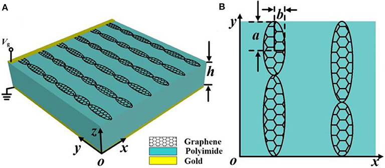
Figure 1. (A) Three-dimensional schematic diagram of the proposed absorber, (B) Top view and geometry of the unit-cell.
Numerical Calculation and Analysis
Figure 2A shows the absorption, transmittance, reflectance spectra in TE-polarized mode under normal incidence. Absorptance can be calculated according to the equation of A = 1-T-R, where T is transmittance T = |S21|2 and R is reflectance R = |S11|2, which can be obtained from simulated S-parameters. From the figure, one can see that the over 90% absorption is from 3.39 to 5.96 THz. Figure 3B displays the real and imaginary parts of the normalized input impedance of the proposed absorber. When the imaginary part of the normalized input impedance of the proposed absorber is zero, the maximum absorption of the absorber can be obtained. At this time, the effective impedance of the absorber matches with the free space impedance (That is to say, the absorber is under impedance matching condition). The effective impedance Z (The impedance is normalized to free space impedance) of the absorber is obtained through the reflection and transmission coefficients and their corresponding phase relationships. The black solid and red solid lines represent the real part and imaginary part of the normalized impedance, respectively. From Figure 2B, one can observed that the real part of the normalized impedance Re(Z) is near 1 and the imaginary part of the normalized impedance Im(Z) is near 0 from 3.39 to 5.96 THz. It indicates that the effective impedance Z of the absorber basically matches the impedance of free space within the bandwidth. The proposed absorber reaches above 92% absorption between 3.39 and 5.96 THz.
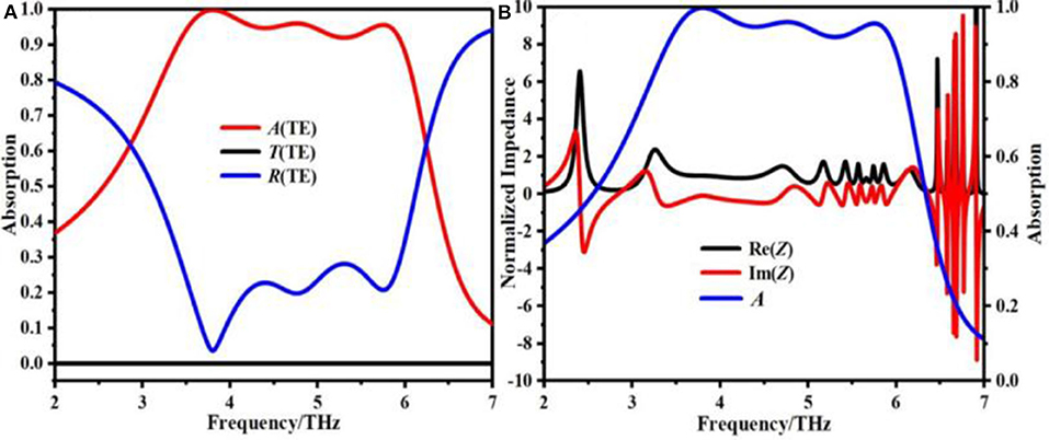
Figure 2. (A) Absorption (A), transmittance (T), and reflectance (R) of the proposed terahertz absorber, (B) real and imaginary parts of the normalized input impedance.
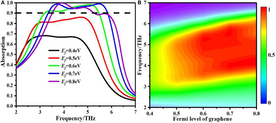
Figure 3. Absorption performance of the absorber with different Fermi levels. (A) Absorption performance of the absorber with different Fermi levels. (B) Absorption spectrum with various Fermi levels.
Figure 3 shows the absorption spectra under different graphene Fermi level Ef. When Fermi level Ef is lower than 0.5 eV, the maximum absorption of the proposed structure is <85%. The average absorption gradually increases when the Fermi level increases to 0.7 eV because of the change of the conductivity. The average absorption performance increases until Ef = 0.7 eV, and it reaches the maximum value of above 95.0%. When Fermi level Ef exceeds 0.7 eV, the absorption effect begins to weaken and average absorption moves downwards. In addition, the bandwidth of the proposed absorber can be tunable by the chemical potentials correspondingly. To study the influence of the structural parameters changes on absorption performance, we systematically change structural parameters (including a, b, and h) to calculate the absorption spectra of the proposed absorber shown in Figure 4. As shown in Figure 4A, with the increase of the semi-major axis a, the absorption peak at 5.0 THz gradually decreases to 88%. When the semi-major axis a equals 5.2 μm, the absorption is above 92% at the frequency range from 3.39 to 5.96 THz. As can be seen from Figure 4B, when the parameter b varies from 2.5 to 4.5 μm, the average absorption has a significant weakening trend. In order to obtain a perfect absorber with above 92% absorption and broad bandwidth from 3.39 to 5.96 THz, we chose the parameter of the semi-minor axis b = 3.5 μm. As depicted in Figure 4C, it is found that as the dielectric layer thickness (h) increases from 8.8 to 9.2 μm, the absorption bandwidth exhibits slightly redshift and average absorption has a slightly weakening trend. When h = 9.0 μm, the absorptance is infinitely close to 100% at f = 6 THz.
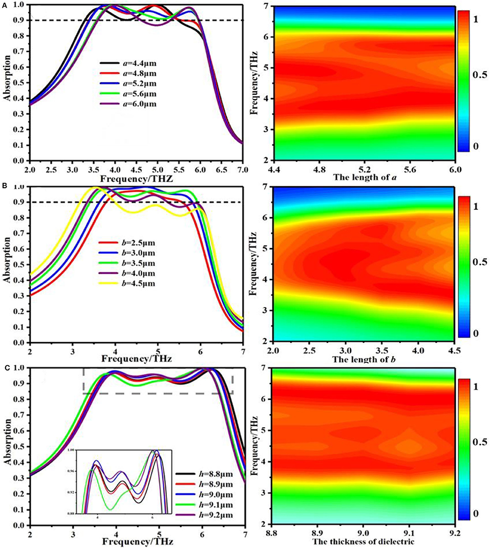
Figure 4. Absorption performance of the absorber with (A) different semi-major axis (B) different semi-minor axis (C) different dielectric layer thicknesses.
Figures 5a,b illustrate the electric field distribution of the absorber under normal incidence of TE-polarization mode terahertz wave at the resonance frequencies of f = 4 THz and f = 6 THz, respectively. It can be observed that the electric field energy is concentrated on both ends of the long axis of the oval-shaped graphene pattern, which means surface plasmon resonances are strongly bounded to both ends of the long axis of the patterned graphene. Figures 6a–h show the magnetic induction lines and magnetic fields of the proposed absorber at f = 4 THz in x-z plane at y = 0 μm, y = 10.4 μm, y = 14.6 μm, and y = 25 μm, respectively. From Figures 6a,g, y = 0 μm and y = 25 μm, one can find that the magnetic induction lines of the graphene layer are symmetrical. Corresponding magnetic field strength diagrams of y = 0 and y = 25 μm are shown in Figures 6b,h. It indicates that the oval-shaped graphene layer generates magnetic resonance and forms two magnetic dipoles, which promotes the terahertz wave absorption. Figures 6c,e depicts the magnetic induction lines of y = 10.4 and y = 14.6 μm, respectively. The corresponding magnetic field diagrams are illustrated in Figures 6d,f, respectively. At y = 10.4 and y = 14.6 μm, the oval-shaped graphene layer forms a single magnetic dipole and promotes the terahertz wave absorption. The magnetic resonance occurs at the long axis of the oval-shaped graphene pattern, and the energy is basically concentrated on the long axis of the oval-shaped graphene pattern.
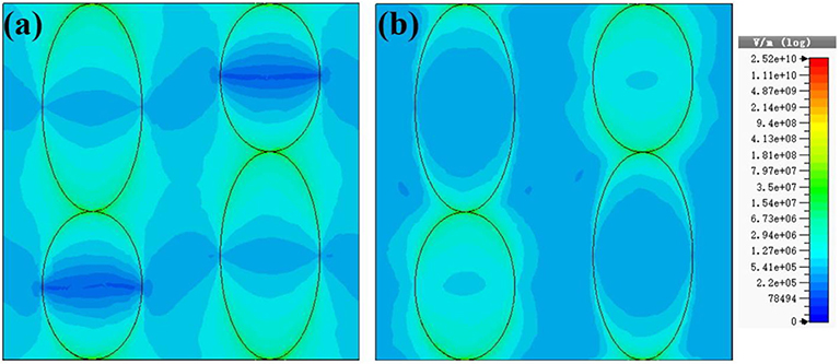
Figure 5. Electric field distribution at (a) f = 4 THz (b) f = 6 THz.
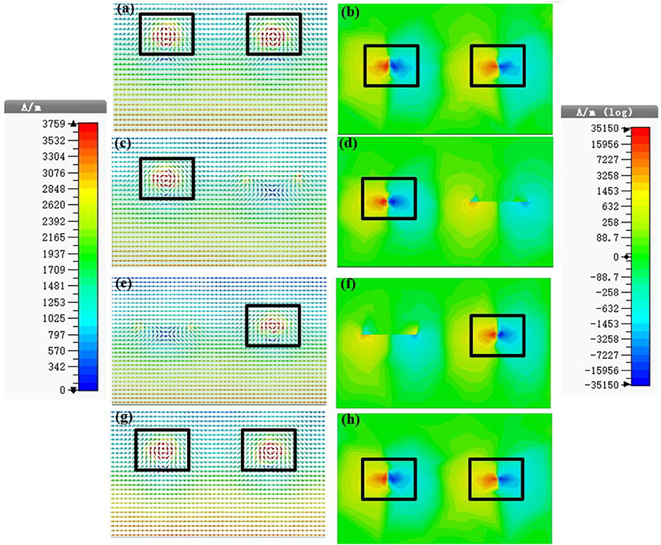
Figure 6. x-z plane and 4 THz, (a,b) are magnetic induction lines and magnetic field diagrams at y = 0 μm, (c,d) are magnetic induction lines and magnetic field diagrams at y = 10.4 μm, (e,f) are magnetic induction lines and magnetic fields at y = 14.6 μm, (g,h) are magnetic induction lines and magnetic fields at y = 25 μm, respectively.
The magnetic induction lines and magnetic field diagrams of the absorber in x-z plane at y = 0, y = 10.4, y = 14.6, and y = 25 μm at a frequency of f = 6 THz are shown in Figure 7. It can be observed that, compared with the Figure 6 (f = 4 THz), the magnetic field strength and magnetic loop position are different. At f = 6 THz, the top graphene pattern has a magnetic resonance but a corresponding magnetic loop is formed in the dielectric layer. Furthermore, the magnetic field strength is weaker than that of f = 4 THz. The absorption spectra of TE polarization mode, operating frequency and incidence angle are plotted in Figures 8A,B. One can see that the absorber has a relatively stable absorptivity (above 92%) with absorption bandwidth from 3.39 to 5.96 THz in the incident angle range of 0–40°. Table 1 shows the performances of our absorber and some reported absorber.
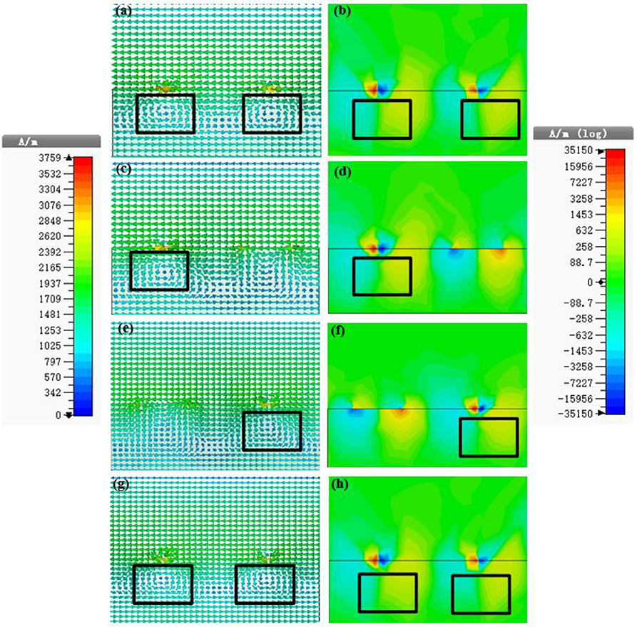
Figure 7. x-z plane and f = 6 THz, (a,b) are magnetic induction lines and magnetic field diagrams at y = 0 μm, (c,d) are magnetic induction line and magnetic field diagrams at y = 14.6 μm, respectively, (e,f) are magnetic induction lines and magnetic field diagrams at y = 10.4 μm, (g,h) are magnetic induction lines and magnetic field diagrams at y = 25 μm, respectively.
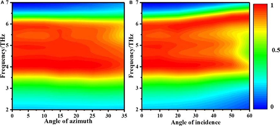
Figure 8. Absorption spectra with different (A) azimuth angles (B) incidence angles.
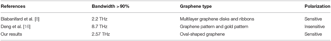
Table 1. Performance comparison of the proposed absorber with some reported absorber.
Conclusion
To sum up, we have numerically studied a broadband tunable absorber based on series asymmetric oval-shaped graphene array. The simulated results indicate that the proposed structure provides a broadband absorption (3.39~5.96 THz) with absorbance higher than 92%. Furthermore, one sees that both the absorption bandwidth and the absorbance of the proposed absorber can be dynamically controlled by changing the Fermi level of the series asymmetric oval-shaped graphene array. The proposed absorber may have potential applications such as filter and switch in terahertz range.
Data Availability Statement
The raw data supporting the conclusions of this article will be made available by the authors, without undue reservation.
Author Contributions
J-ZS performed the calculations. J-SL concerned the devices structure and developed the theoretical model. All authors discussed the results and co-wrote the manuscript.
Funding
This work was sponsored by Natural Science Foundation of Zhejiang Province (LY18F010016), National Natural Science Foundation of China (Grant Nos. 61871355 and 61831012) and Zhejiang Lab (No. 2019LC0AB03).
Conflict of Interest
The authors declare that the research was conducted in the absence of any commercial or financial relationships that could be construed as a potential conflict of interest.
Acknowledgments
We would like to thank X. Chen for his help and support.
References
1. Kuznetsov S, Paulish A, Gelfand A, Lazorskiy P, Fedorinin V. Bolometric THz-to-IR converter for terahertz imaging. Appl Phys Lett. (2011) 99:710. doi: 10.1063/1.3607474
2. Liu N, Mesch M, Weiss T, Hentschel M, Giessen H. Infrared perfect absorber and its application as plasmonic sensor. Nano Lett. (2010) 10:2342–8. doi: 10.1021/nl9041033
3. He G, Stiens J. Enhanced terahertz absorption of graphene composite integrated with double circular metal ring array. Plasmonics. (2017) 9:1–6. doi: 10.1007/s11468-017-0682-2
4. Xu Y, Li E, Wei X, Yi D. A novel tunable absorber based on vertical graphene strips. IEEE Microw Wireless Compon Lett. (2016) 26:10–2. doi: 10.1109/LMWC.2015.2505610
5. Fu P, Liu F, Ren G, Fei S, Dong L, Jian Y. A broadband metamaterial absorber based on multi-layer graphene in the terahertz region. Opt Commun. (2018) 417:62–6. doi: 10.1016/j.optcom.2018.02.034
6. Zhu Z, Guo C, Zhang J, Liu K, Yun X, Qin S. Broadband single-layered graphene absorber using periodic arrays of graphene ribbons with gradient width. Appl Phys Express. (2015) 8:015102. doi: 10.7567/APEX.8.015102
7. Andryieuski Lavrinenko A. Graphene metamaterials based tunable terahertz absorber: effective surface conductivity approach. Opt Express. (2013) 21:9144–55. doi: 10.1364/OE.21.009144
8. Sadegh Mohammad B, Somayyeh A, Shahrouz A, Mustapha Y. Tunable ultra-wideband terahertz absorber based on graphene disks and ribbons. Opt Commun. (2018) 427:418–25. doi: 10.1016/j.optcom.2018.07.008
9. Lei L, Lou F, Tao K, Huang H, Cheng X, Xu P. Tunable and scalable broadband metamaterial absorber involving VO2-based phase transition. Photon Res. (2019) 7:734–41. doi: 10.1364/PRJ.7.000734
10. Kenney M, Grant J, Shah Y, Carranza I, Humphreys M, Cumming D. Octave-spanning broadband absorption of terahertz light using metasurface fractal-cross absorbers. ACS Photonics. (2017) 4:2604–12. doi: 10.1021/acsphotonics.7b00906
11. Grant J, Ma Y, Saha S, Khalid A, Cumming D. Polarization insensitive broadband terahertz metamaterial absorber. Opt Lett. (2011) 36:3476–8. doi: 10.1364/OL.36.003476
12. Wang B, Wang L, Wang G, Huang W, Li X, Zhai X. Metamaterial based low-conductivity alloy perfect absorber. J Lightwave Technol. (2014) 32:2293–8. doi: 10.1109/JLT.2014.2322860
13. Pu M, Wang M, Hu C, Huang C, Zhao Z, Wang Y, et al. Engineering heavily doped silicon for broadband absorber in the terahertz regime. Opt Express. (2012) 20:25513–9. doi: 10.1364/OE.20.025513
14. Cheng YZ, Withayachumnankul W, Upadhyay A, Headland D, Nie Y, Gong R, et al. Ultrabroadband plasmonic absorber for terahertz waves. Adv Opt Mater. (2015) 3:376–80. doi: 10.1002/adom.201400368
15. Rahmanzadeh M, Rajabalipanah H, Abdolali A. Multilayer graphene-based metasurfaces: robust design method for extremely broadband, wide-angle, and polarization-insensitive terahertz absorbers. Appl Opt. (2018) 57:959. doi: 10.1364/AO.57.000959
Keywords: terahertz absorption, asymmetric oval-shaped graphene, wide-incident-angle, graphene, broadband
Citation: Sun J-Z and Li J-S (2020) Broadband Adjustable Terahertz Absorption in Series Asymmetric Oval-Shaped Graphene Pattern. Front. Phys. 8:245. doi: 10.3389/fphy.2020.00245
Received: 02 May 2020; Accepted: 03 June 2020;
Published: 15 July 2020.
Edited by:
Haiyong Gan, National Institute of Metrology, ChinaReviewed by:
Weien Lai, Hefei University of Technology, ChinaFuri Ling, Huazhong University of Science and Technology, China
Shuyun Teng, Shandong Normal University, China
Copyright © 2020 Sun and Li. This is an open-access article distributed under the terms of the Creative Commons Attribution License (CC BY). The use, distribution or reproduction in other forums is permitted, provided the original author(s) and the copyright owner(s) are credited and that the original publication in this journal is cited, in accordance with accepted academic practice. No use, distribution or reproduction is permitted which does not comply with these terms.
*Correspondence: Li Jiu-Sheng, anNobGlAMTI2LmNvbQ==