 Anbo Feng1
 Wei Zhu
- 1State Key Laboratory of Crystal Materials, Institute of Crystal Materials, Shandong University, Jinan, China
- 2Institute of Radiation Medicine, Shandong Academy of Medical Sciences, Shandong First Medical University, Jinan, China
Metal halide perovskite single crystals are a promising candidate for X-ray detection due to their large atomic number and high carrier mobility and lifetime. However, it is still challenging to grow large-area and thin single crystals directly onto substrates to meet real-world applications. In this work, millimeter-thick and inch-sized methylammonium lead tribromide (MAPbBr3) single-crystal wafers are grown directly on indium tin oxide (ITO) substrates through controlling the distance between solution surface and substrates. The single-crystal wafers are polished and treated with O3 to achieve smooth surface, lower trap density, and better electrical properties. X-ray detectors with a high sensitivity of 632 µC Gyair−1 cm−2 under –5 V and 525 µC Gyair−1 cm−2 under –1 V bias can be achieved. This work provides an effective way to fabricate substrate-integrated, large-area, and thickness-controlled perovskite single-crystal X-ray detectors, which is instructive for developing imaging application based on perovskite single crystals.
Introduction
In recent years, metal halide perovskite (MHP) materials have been demonstrated as promising candidates for sensitive X-ray detections due to their superior properties (Li Z et al., 2021), such as large atomic number, high carrier mobility and lifetime, and low-defect density (Wei et al., 2017; Cheng et al., 2019; Chen et al., 2019). There are two kinds of perovskite X-ray detectors: direct and indirect detection modes (Zhou et al., 2020). Compared to indirect detection which converts X-ray to a light signal, the direct detection mode which converts X-ray to an electrical signal has larger spatial resolution and higher sensitivity (Basiricò et al., 2019). Because of the strong stopping power and superior spatial resolution in X-ray, α-Se dominates direct conversion X-ray imaging, such as computed tomography (CT). But α-Se detectors have low sensitivity and require high dose for imaging, which brings cancer risk to the patients (Kasap et al., 2000). In comparison, the sensitivity of perovskite X-ray detectors are several orders of magnitude larger than that of commercial α-Se detectors, especially for hard X-ray (Wang et al., 2020; Deumel et al., 2021; Liu et al., 2021a; Peng et al., 2021).
Current state-of-the-art perovskite X-ray detectors are mainly made of bulk single crystals, which possess better electrical properties and higher stability than their polycrystalline counterparts due to the absence of grain boundaries (Wei et al., 2017; Liu et al., 2018; Yao et al., 2020; Liu et al., 2021b). Perovskite single crystals can be grown by the low-cost solution-based method, which is compatible with Si-based application-specific integrated circuits for signal readout (Wei et al., 2017; Geng et al., 2020). In general, perovskite single crystals with millimeter-sized thickness are in principle enough to fully attenuate the incident hard X-ray that is predominantly applied in medical imaging areas (Song et al., 2020). However, perovskite single crystals show weak anisotropic growth, leading to large crystal thickness, which not only reduces the vertical carrier collection yield but can also cause undesired cross-talk between pixels (Zhuang et al., 2019). To avoid these drawbacks, high-working bias is required to strengthen the vertical carrier collection (Li et al., 2020). Nevertheless, the monovalent ions in perovskite materials are prone to migrate under bias, which can cause fluctuation of dark and signal currents (Shao et al., 2016; Pan et al., 2017). Recently, highly sensitive and self-powered perovskite X-ray detectors are achieved through finely controlling crystal thickness and optimizing the carrier transport properties, which represents an effective way to eliminate ion migration and cross-talk between pixels (Wu et al., 2021). Another challenge comes from the lack of an established method to grow thin single crystals with size comparable to bulk crystals (Kim et al., 2017). In this case, it is important to develop an effective method to grow inch-sized thin perovskite single crystals and integrate them with substrates to meet real-world applications.
In this work, we report sensitive X-ray detectors made of millimeter-thick and inch-sized MAPbBr3 single-crystal wafers. The MAPbBr3 single-crystal wafers are directly grown on indium tin oxide (ITO) substrates, and the thickness is controlled by the distance between solution surface and substrates. O3-UV exposure has been used for the post-procedure in order to passivate traps on the single-crystal surface (Wei et al., 2016; Yao et al., 2021). Eventually, X-ray detectors with a high sensitivity of 632 µC Gyair−1 cm−2 under −5 V and 525 µC Gyair−1 cm−2 under −1 V bias can be achieved. This work provides an effective way to fabricate substrate-integrated, large-area, and thickness-controlled perovskite single-crystal X-ray detectors, which is beneficial to meet real-world applications.
Materials and Methods
Chemicals and reagents: Methylamine (CH3NH2) (40 wt% in water), hydrobromic acid (HBr) (40 wt% in water), and lead bromide were obtained from stannic iodide produced by Xi’an Polymer Light Technology. N, N-Dimethylformamide (DMF, 99%) was purchased from Aladdin Reagent Ltd. Fullerene (C60), and 2,9-dimethyl-4,7-diphenyl-1,10-phenathroline (BCP) and poly (3,4-ethylenedioxythiophene)/poly (styrenesulfonate) PEDOT: PSS were purchased from Xi’an Polymer Light Technology.
Synthesis of Methylammonium Bromide (CH3NH3Br): CH3NH3Br was synthesized on the basis of the previously reported method in which HBr and CH3NH2 were reacted with the molar ratio of 1:1.2. To be specific, 125 ml of methylamine (40% in ethanol) was first put in a 1,000-ml round bottom flask under an ice bath; subsequently, 125 ml hydrobromic acid (40 wt% in water) was added drop by drop; in case a severe reaction took place between them, the mixture was made to react under constant stirring for 6 h. The initial CH3NH3Br product was collected by evaporating the mixture using the rotary evaporator at 60°C. Then, the initial powder was washed by absolute ethyl alcohol three times and anhydrous ethyl ether three times. Finally, the white CH3NH3Br powder was obtained by recrystallization in anhydrous diethyl ether for half an hour and then dried in a vacuum oven at 60°C for 12 h.
Growth of substrate-integrated MAPbBr3 thin single-crystal wafers: Initially, a small MAPbBr3 crystal seed was grown by the inverse temperature crystallization (ITC) method. Subsequently, the crystal seed was put on PEDOT: PSS-covered ITO substrates and then immersed into a saturated solution to promote further growth of the crystal seed until the desired size was reached. The crystal thickness was controlled by the distance between the substrate and solution surface precisely.
X-ray Detector Device Fabrication: C60 (40 nm) and BCP (3 nm) were thermally evaporated at a rate of 0.2 Å/s to form the charge transport layer. Cu (80 nm) was thermally evaporated at a rate of 0.8 Å/s to form the electrode.
Characterizations
Powder X-ray diffraction (PXRD) patterns were measured on a SmartLab SE High-Resolution Diffraction System with Cu Kα1 radiation (λ = 1.54186Å) in the range of 5–90°(2θ) with a single-crystal thin film of 2 × 1 × 0.02 mm3 in size. Scanning electron microscope (SEM): The surface and cross morphology images were taken from a field emission microscope (Phenom Pharos). Steady-state absorption: Absorption spectra were determined using a U3500 Hitachi UV/Vis Spectrophotometer with the self-made testing mold. Device I-V characteristics were collected by using a Keithley 2,400 analyzer. AM 1.5-G irradiation (100 mW/cm2) was produced by a xenon-lamp–based solar simulator. X-ray was generated by an Amptek Mini-X2 tube with an Ag target, whose characteristic Kα peak is 22 keV. The X-ray dose rate was calibrated by a Radcal Accu-Gold+ 10X6-180 ion chamber dosimeter.
Results and Discussion
MAPbBr3 is a prototype perovskite material for X-ray detection application and therefore was selected for our investigation. To grow thickness-controlled perovskite single crystals, a space-confined strategy has been widely adopted (Liu et al., 2016; Chen et al., 2017; Alsalloum et al., 2021). But, the slow ion diffusion rate in the confined space can cause small crystal size and poor crystal quality (Cheng et al., 2019). Here, we try to control the crystal thickness by adjusting the distance between the solution surface and substrate, as illustrated in Figure 1A. Initially, a small MAPbBr3 crystal seed was obtained by the ITC method in which solubility decreases with increasing temperature. Subsequently, the crystal seed was put on PEDOT: PSS-covered ITO substrates and then immersed into a saturated solution to promote further growth of the crystal seed. To obtain high-quality single crystals, the temperature was increased slowly with a rate of 1°C/h to ensure the solution concentration was located in the metastable region. The vertical growth will stop when the single crystal is close to the solution surface while the lateral growth is not limited, thus resulting in thickness-controlled and inch-sized single-crystal wafers.
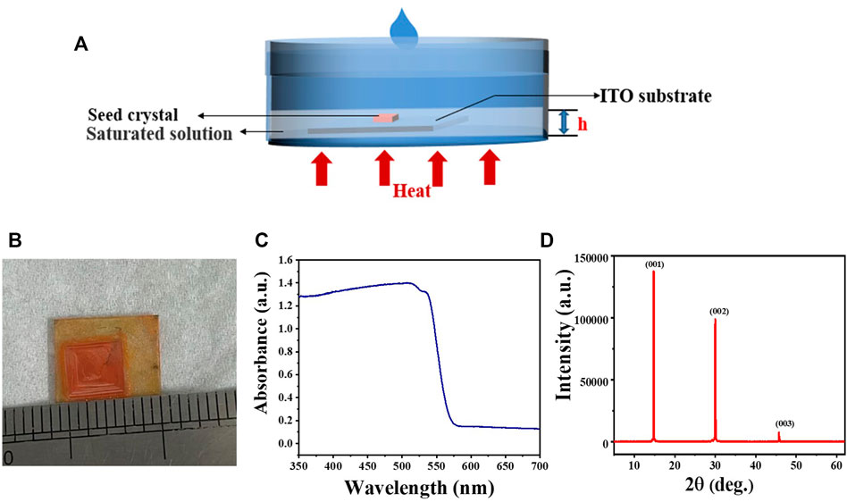
FIGURE 1. (A) Schematic illustration of the MAPbBr3 single-crystal wafer growth process. (B) Photograph of the as-grown single-crystal wafer attached to the ITO glass. (C) UV-Vis–NIR absorption spectra. (D) XRD pattern of the MAPbBr3 single-crystal wafer.
As shown in Figure 1B, the as-grown MAPbBr3 single-crystal wafers are square and semitransparent, indicating their high crystal quality. The lateral size of the single-crystal wafer is nearly 1 cm, and the thickness can be controlled at millimeter scale. The basic properties of the single-crystal wafers are characterized by UV-vis absorption and X-ray diffraction (XRD). As shown in Figure 1C, the absorption onset is 575 nm, which is consistent with previously reported values (Zhang et al., 2020). The XRD patterns show sharp diffraction peaks at 14.92°, 30.07°, and 45.77°, which can be assigned to (001), (002), and (003) planes (Figure 1D), suggesting that the exposed face of the single-crystal wafers is the (001) crystal plane. These results clearly show the successful growth of thin MAPbBr3 single-crystal wafers.
X-ray with different photon energy levels has different penetration depths and requires different crystal thicknesses (Wei et al., 2016). To adjust the thickness of the single-crystal wafers, the distance between the substrate and solution surface is tuned. Figure 2A shows the photographs of MAPbBr3 single-crystal wafers with different thickness, which have similar shape and lateral size (Figure 2B). The crystal thickness can be controlled from ∼1 to ∼3.5 mm, satisfying full attenuation of soft and hard X-ray, respectively (Wei et al., 2016). Intimate interface contact is necessary for effective interface carrier injection and high X-ray response. To investigate the interface contact between the MAPbBr3 single-crystal wafers and ITO substrates, cross-sectional SEM measurement is conducted. As shown in Figure 2C, no voids and rain boundaries are observed between the MAPbBr3 single-crystal wafers and ITO substrates, confirming an intimate contact and single-crystalline character.
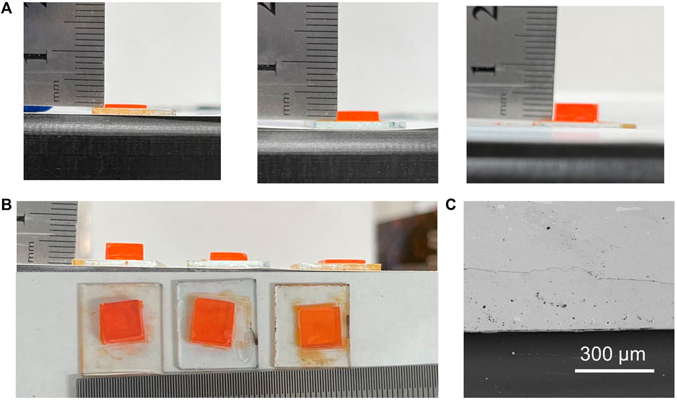
FIGURE 2. (A) Photographs of the as-grown MAPbBr3 single crystals with thicknesses differing from 1 to 3.5 mm. (B) Different thicknesses of the single crystal with similar size. (C) Cross-sectional SEM images of the MAPbBr3 single-crystal wafer.
From the photograph and top-view SEM image (Figures 3A,B), we find that a deep valley is observed on the surface of the as-grown MAPbBr3 single-crystal wafers, which will make it challenging for the continuous electrode. To overcome this problem, the crystal surface is polished by using 10,000-mesh sandpaper. It can be found that the crystal surface becomes relatively smooth after the polishing process, and the single-crystal wafers are still semitransparent (Figures 3C,D). The smooth surface can ensure deposition of the continuous electrode, which is important for electrical characterization and device fabrication.
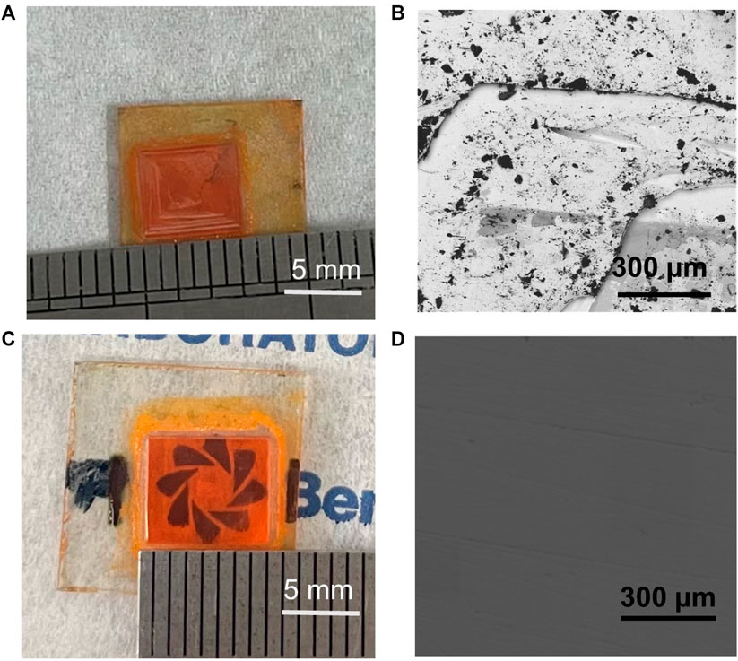
FIGURE 3. (A)–(B) Photograph and top view SEM of the as-grown single crystal. (C)–(D) Photograph and top view SEM of the polished single crystal.
Low-defect density and superior carrier transport properties are important for high sensitivity of the detector devices. The surface trap passivation of the polished MAPbBr3 single-crystal wafers is conducted by O3–UV treatment. Photoluminescence was first conducted to preliminarily assess the trap passivation, as shown in Figure 4A; the PL intensity of the single-crystal wafer after 5 min of O3–UV exposure is stronger than that of the untreated sample, which can be attributed to the decrease of uncoordinated Pb atoms on the crystal surface; O3–UV exactly acts the role of the trap passivation during this process. Nevertheless, long-time exposure of O3–UV may bring about severe ion migration that is why PL intensity decreases after 10 min of O3–UV exposure (Li W et al., 2021). To obtain further analysis, the hole carrier mobility and carrier lifetime were measured by the transient time-resolved photoluminescence method (Figure 4B) and space charge limited current (SCLC) (Figures 4C,D). The hole-only devices with the structure of ITO/PEDOT: PSS/single crystals/Au were fabricated (Figures 4C,D inset). The carrier mobility and trap density are calculated based on Equation 1 and Equation 2, respectively (Kim et al., 2020):
where JD is the dark current density, ε is the dielectric constant of perovskite single crystals, ε0 is the dielectric constant of vacuum, μ is the mobility, Vb is the bias, and L is the crystal thickness (Zhang et al., 2018).
where VTFL is the voltage at which all the traps are filled, e is the elementary charge, and nt is the hole trap density. Without O3 treatment, the hole mobility and trap density are calculated to be 51 cm2 V−1 s−1 and 2.59
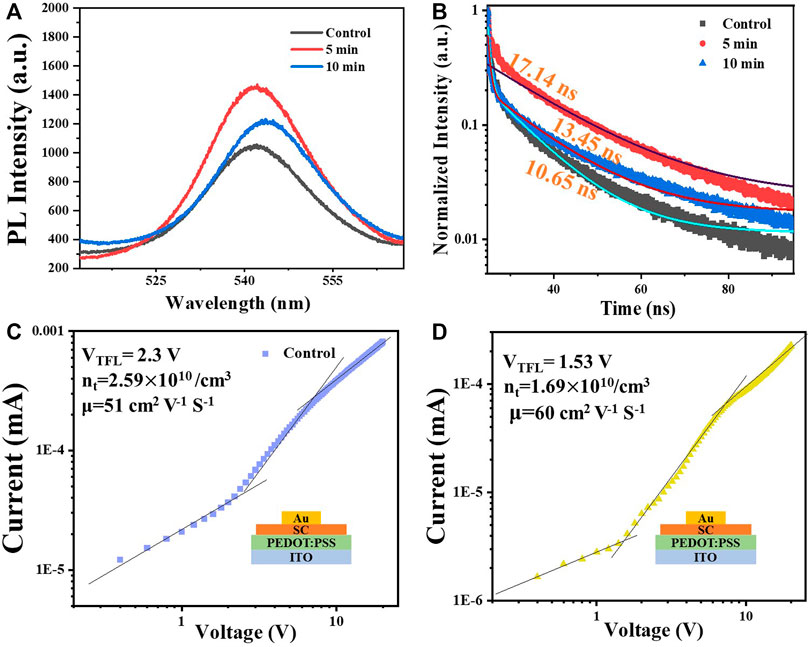
FIGURE 4. (A) Photoluminescence spectra and (B) time-resolved photoluminescence of the control sample and sample after O3–UV exposure for 5 and 10 min. (C)–(D) Space charge limited current (SCLC) measurement for the control and 5 min O3–UV-treated sample, and the structures of hole-only devices are displayed inset.
It is obvious that O3 treatment enhances the optoelectronic properties of MAPbBr3 single-crystal wafers, which will improve the detector performance. To confirm this point, detectors with a structure of ITO/PEDOT: PSS/single crystals/C60/BCP/copper (Cu) are constructed (Figure 5A). The energy diagram of the device is shown in Figure 5B, which indicates that the insertion of the PEDOT: PSS hole transport layer and C60/BCP electron transport layer can facilitate the charge extraction. The detectors show a narrowband photo-response with a peak value in the below-bandgap absorption, similar to previously reported photodetectors based on bulk perovskite crystals. The relatively low response in the above-bandgap region is due to small penetration length and surface charge recombination. Figures 5C,D show the current density–voltage (J–V) curves of the detectors under dark and AM 1.5 illumination. Compared to the control detectors, the detectors with O3 treatment show a lower dark current and larger photocurrent, which is consistent with the results of lower trap density.
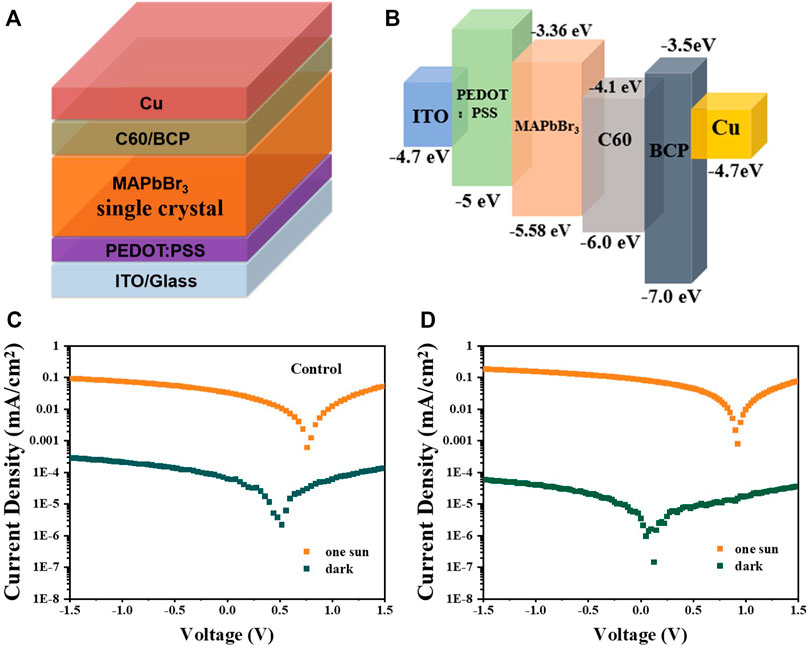
FIGURE 5. (A) Schematic structure and (B) energy band diagram of the MAPbBr3 single crystal–based device. Control (C) and O3–UV-treated (D) detectors under dark and AM 1.5 illumination.
Finally, the X-ray response properties of the detectors by continuously turning on and off the X-ray source are evaluated. The X-ray response performance of the single-crystal devices was tested under an X-ray source with energy up to 50 keV and peak intensity at 50 keV. Due to their better electrical transport properties, the X-ray response of detectors with O3 treatment is distinctly stronger than that of control devices under various bias (Figures 6A,B). Besides, it is worth noting that the dark current and photocurrent of detectors with O3 treatment are more stable than those of control devices, especially when the bias is increased. The smaller drift of the dark and signal current indicates ion migration is weakened after O3 treatment, which is consistent with the reduced trap density. Figures 6C,D summarize the photocurrent of the two single-crystal detectors under various dose rates and bias. A high sensitivity of 632 µC Gyair−1 cm−2 under –5 V and 525 µC Gyair−1 cm−2 under –1 V is obtained for the optimal devices, which surpasses that of commercial α-Se X-ray detectors.
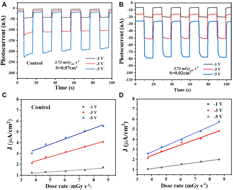
FIGURE 6. X-ray response of the control device (A) and O3–UV-treated device (B) under various bias. (C)–(D) Summary of the photocurrent of the two single-crystal detectors under various dose rates and bias.
Conclusion
In conclusion, we develop an effective method to grow substrate-integrated, thickness-controlled, and inch-sized perovskite single crystals, which can help to reduce cross-talk between pixels and enhance vertical carrier collection. The crystal thickness can be adjusted to satisfy full attenuation of soft and hard X-ray. After polishing and O3 treatment, the optoelectronic properties can be improved, leading to an enhanced X-ray response. A high sensitivity of 632 µC Gair−1 cm−2 under –5V and 525 µC Gyair−1 cm−2 under –1 V is obtained for the optimal devices.
Data Availability Statement
The original contributions presented in the study are included in the article/Supplementary Material; further inquiries can be directed to the corresponding author.
Author Contributions
ZC, XF, and WZ devised the project and proof outline. AF and SX grew the MAPbBr3 single-crystal wafers directly on the ITO glass and conducted all mentioned characterizations. All authors contributed to manuscript revision and read and approved the submitted version.
Funding
This work was funded by the National Natural Science Foundation of China (Grant No. 52002221), Natural Science Foundation of Jiangsu Province (BK20200230), and Natural Science Foundation of Shandong Province (ZR2020QE059).
Conflict of Interest
The authors declare that the research was conducted in the absence of any commercial or financial relationships that could be construed as a potential conflict of interest.
Publisher’s Note
All claims expressed in this article are solely those of the authors and do not necessarily represent those of their affiliated organizations, or those of the publisher, the editors, and the reviewers. Any product that may be evaluated in this article, or claim that may be made by its manufacturer, is not guaranteed or endorsed by the publisher.
References
Alsalloum, A. Y., Turedi, B., Almasabi, K., Zheng, X., Naphade, R., Stranks, S. D., et al. (2021). 22.8%-efficient Single-crystal Mixed-Cation Inverted Perovskite Solar Cells with a Near-Optimal Bandgap. Energ. Environ. Sci. 14, 2263–2268. doi:10.1039/d0ee03839c
Basiricò, L., Senanayak, S. P., Ciavatti, A., Abdi‐Jalebi, M., Fraboni, B., and Sirringhaus, H. (2019). Detection of X‐Rays by Solution‐Processed Cesium‐Containing Mixed Triple Cation Perovskite Thin Films. Adv. Funct. Mater. 29, 1902346. doi:10.1002/adfm.201902346
Chen, Z., Turedi, B., Alsalloum, A. Y., Yang, C., Zheng, X., Gereige, I., et al. (2019). Single-crystal Mapbi3 Perovskite Solar Cells Exceeding 21% Power Conversion Efficiency. ACS Energ. Lett. 4, 1258–1259. doi:10.1021/acsenergylett.9b00847
Chen, Z., Dong, Q., Liu, Y., Bao, C., Fang, Y., Lin, Y., et al. (2017). Thin Single crystal Perovskite Solar Cells to Harvest Below-Bandgap Light Absorption. Nat. Commun. 8, 1890. doi:10.1038/s41467-017-02039-5
Cheng, X., Yang, S., Cao, B., Tao, X., and Chen, Z. (2019). Single crystal Perovskite Solar Cells: Development and Perspectives. Adv. Funct. Mater. 30, 1905021. doi:10.1002/adfm.201905021
Deumel, S., van Breemen, A., Gelinck, G., Peeters, B., Maas, J., Verbeek, R., et al. (2021). High-sensitivity High-Resolution X-ray Imaging with Soft-Sintered Metal Halide Perovskites. Nat. Electron. 4, 681–688. doi:10.1038/s41928-021-00644-3
Geng, X., Wang, F., Tian, H., Feng, Q., Zhang, H., Liang, R., et al. (2020). Ultrafast Photodetector by Integrating Perovskite Directly on Silicon Wafer. ACS nano 14, 2860–2868. doi:10.1021/acsnano.9b06345
Kasap, S. O., Haugen, C., Nesdoly, M., and Rowlands, J. A. (2000). Properties of A-Se for Use in Flat Panel X-ray Image Detectors. J. Non-Crystalline Sol. 266-269, 1163–1167. doi:10.1016/s0022-3093(99)00954-0
Kim, H., Lee, J. W., Han, G. R., Kim, S. K., and Oh, J. H. (2020). Synergistic Effects of Cation and Anion in an Ionic Imidazolium Tetrafluoroborate Additive for Improving the Efficiency and Stability of Half‐Mixed Pb‐Sn Perovskite Solar Cells. Adv. Funct. Mater. 31, 2008801. doi:10.1002/adfm.202008801
Kim, Y. C., Kim, K. H., Son, D.-Y., Jeong, D.-N., Seo, J.-Y., Choi, Y. S., et al. (2017). Printable Organometallic Perovskite Enables Large-Area, Low-Dose X-ray Imaging. Nature 550, 87–91. doi:10.1038/nature24032
Li, H., Song, J., Pan, W., Xu, D., Zhu, W. a., Wei, H., et al. (2020). Sensitive and Stable 2D Perovskite Single‐Crystal X‐ray Detectors Enabled by a Supramolecular Anchor. Adv. Mater. 32, 2003790. doi:10.1002/adma.202003790
Li W, W., Li, H., Song, J., Guo, C., Zhang, H., Wei, H., et al. (2021). Fine-control-valve of Halide Perovskite Single crystal Quality for High Performance X-ray Detection. Sci. Bull. 66, 2199–2206. doi:10.1016/j.scib.2021.06.016
Li Z, Z., Zhou, F., Yao, H., Ci, Z., Yang, Z., and Jin, Z. (2021). Halide Perovskites for High-Performance X-ray Detector. Mater. Today 48, 155–175. doi:10.1016/j.mattod.2021.01.028
Liu, Y., Zhang, Y., Yang, Z., Yang, D., Ren, X., Pang, L., et al. (2016). Thinness- and Shape-Controlled Growth for Ultrathin Single-Crystalline Perovskite Wafers for Mass Production of superior Photoelectronic Devices. Adv. Mater. 28, 9204–9209. doi:10.1002/adma.201601995
Liu, Y., Zhang, Y., Zhao, K., Yang, Z., Feng, J., Zhang, X., et al. (2018). A 1300 mm2Ultrahigh-Performance Digital Imaging Assembly Using High-Quality Perovskite Single Crystals. Adv. Mater. 30, 1707314. doi:10.1002/adma.201707314
Liu, Y., Zhang, Y., Zhu, X., Feng, J., Spanopoulos, I., Ke, W., et al. (2021b). Triple‐Cation and Mixed‐Halide Perovskite Single Crystal for High‐Performance X‐ray Imaging. Adv. Mater. 33, 2006010. doi:10.1002/adma.202006010
Liu, Y., Zheng, X., Fang, Y., Zhou, Y., Ni, Z., Xiao, X., et al. (2021a). Ligand Assisted Growth of Perovskite Single Crystals with Low Defect Density. Nat. Commun. 12, 1686. doi:10.1038/s41467-021-21934-6
Pan, W., Wu, H., Luo, J., Deng, Z., Ge, C., Chen, C., et al. (2017). Cs2agbibr6 Single-crystal X-ray Detectors with a Low Detection Limit. Nat. Photon 11, 726–732. doi:10.1038/s41566-017-0012-4
Peng, J., Xia, C. Q., Xu, Y., Li, R., Cui, L., Clegg, J. K., et al. (2021). Crystallization of Cspbbr3 Single Crystals in Water for X-ray Detection. Nat. Commun. 12, 1531. doi:10.1038/s41467-021-21805-0
Shao, Y., Fang, Y., Li, T., Wang, Q., Dong, Q., Deng, Y., et al. (2016). Grain Boundary Dominated Ion Migration in Polycrystalline Organic-Inorganic Halide Perovskite Films. Energy Environ. Sci. 9, 1752–1759. doi:10.1039/c6ee00413j
Song, Y., Li, L., Bi, W., Hao, M., Kang, Y., Wang, A., et al. (2020). Atomistic Surface Passivation of CH3NH3PbI3 Perovskite Single Crystals for Highly Sensitive Coplanar-Structure x-Ray Detectors. Research, 10. doi:10.34133/2020/5958243
Wang, X., Li, Y., Xu, Y., Pan, Y., Zhu, C., Zhu, D., et al. (2020). Solution-processed Halide Perovskite Single Crystals with Intrinsic Compositional Gradients for X-ray Detection. Chem. Mater. 32, 4973–4983. doi:10.1021/acs.chemmater.9b05000
Wei, H., Fang, Y., Mulligan, P., Chuirazzi, W., Fang, H.-H., Wang, C., et al. (2016). Sensitive X-ray Detectors Made of Methylammonium lead Tribromide Perovskite Single Crystals. Nat. Photon 10, 333–339. doi:10.1038/nphoton.2016.41
Wei, W., Zhang, Y., Xu, Q., Wei, H., Fang, Y., Wang, Q., et al. (2017). Monolithic Integration of Hybrid Perovskite Single Crystals with Heterogenous Substrate for Highly Sensitive X-ray Imaging. Nat. Photon 11, 315–321. doi:10.1038/nphoton.2017.43
Wu, J., Wang, L., Feng, A., Yang, S., Li, N., Jiang, X., et al. (2021). Self‐Powered FA 0.55 MA 0.45 PbI 3 Single‐Crystal Perovskite X‐Ray Detectors with High Sensitivity. Adv. Funct. Mater., 2109149. doi:10.1002/adfm.202109149
Yao, F., Peng, J., Li, R., Li, W., Gui, P., Li, B., et al. (2020). Room-temperature Liquid Diffused Separation Induced Crystallization for High-Quality Perovskite Single Crystals. Nat. Commun. 11, 1194. doi:10.1038/s41467-020-15037-x
Yao, M., Jiang, J., Xin, D., Ma, Y., Wei, W., Zheng, X., et al. (2021). High-temperature Stable Fapbbr3 Single Crystals for Sensitive X-ray and Visible Light Detection toward Space. Nano Lett. 21, 3947–3955. doi:10.1021/acs.nanolett.1c00700
Zhang, L., Cui, S., Guo, Q., Ge, C., Han, Q., Lin, Q., et al. (2020). Anisotropic Performance of High-Quality Mapbbr3 Single-crystal Wafers. ACS Appl. Mater. Inter. 12, 51616–51627. doi:10.1021/acsami.0c14582
Zhang, P., Zhang, G., Liu, L., Ju, D., Zhang, L., Cheng, K., et al. (2018). Anisotropic Optoelectronic Properties of Melt-Grown Bulk Cspbbr3 Single crystal. J. Phys. Chem. Lett. 9, 5040–5046. doi:10.1021/acs.jpclett.8b01945
Zhou, F., Li, Z., Lan, W., Wang, Q., Ding, L., and Jin, Z. (2020). Halide Perovskite, a Potential Scintillator for X‐Ray Detection. Small Methods 4, 2000506. doi:10.1002/smtd.202000506
Keywords: perovskite single crystals, X-ray detectors, single-crystal wafers, sensitivity, integration
Citation: Feng A, Xie S, Fu X, Chen Z and Zhu W (2022) Inch-Sized Thin Metal Halide Perovskite Single-Crystal Wafers for Sensitive X-Ray Detection. Front. Chem. 9:823868. doi: 10.3389/fchem.2021.823868
Received: 28 November 2021; Accepted: 10 December 2021;
Published: 05 January 2022.
Edited by:
Dianxing Ju, Qingdao University of Science and Technology, ChinaCopyright © 2022 Feng, Xie, Fu, Chen and Zhu. This is an open-access article distributed under the terms of the Creative Commons Attribution License (CC BY). The use, distribution or reproduction in other forums is permitted, provided the original author(s) and the copyright owner(s) are credited and that the original publication in this journal is cited, in accordance with accepted academic practice. No use, distribution or reproduction is permitted which does not comply with these terms.
*Correspondence: Wei Zhu, ZnNzendAMTYzLmNvbQ==; Zhaolai Chen, emhhb2wuY2hlbjg5MDlAZ21haWwuY29t; Xiuwei Fu, Znh3QHNkdS5lZHUuY24=