 Muhammad Rizwan Saleem
 Rizwan Ali
 Mohammad Bilal Khan
 Seppo Honkanen1
- 1Institute of Photonics, University of Eastern Finland, Joensuu, Finland
- 2Center for Energy Systems (CES), USAID Center for Advance Studies, National University of Sciences and Technology (NUST), Islamabad, Pakistan
We review the significance of optical thin films by Atomic Layer Deposition (ALD) method to fabricate nanophotonic devices and structures. ALD is a versatile technique to deposit functional coatings on reactive surfaces with conformal growth of compound materials, precise thickness control capable of angstrom resolution, and coverage of high aspect ratio nano-structures using wide range of materials. ALD has explored great potential in the emerging fields of photonics, plasmonics, nano-biotechnology, and microelectronics. ALD technique uses sequential reactive chemical reactions to saturate a surface with a monolayer by pulsing of a first precursor (metal alkoxides or covalent halides), followed by reaction with second precursor molecules such as water to form the desired compound coatings. The targeted thickness of the desired compound material is controlled by the number of ALD-cycles of precursor molecules that ensures the self-limiting nature of reactions. The conformal growth and filling of TiO2 and Al2O3 optical materials on nano-structures and their resulting optical properties have been described. The low temperature ALD-growth on various replicated sub-wavelength polymeric gratings is discussed.
1. Introduction
Thin film deposition techniques have been significantly stimulated by the advancement in the high-tech applications in optical systems (Pedrotti, 1993; Macleod, 2001). Dielectric transparent optical thin films in conventional optical filters select a spectral range of transmitted or reflected light such as anti reflecting coatings, pass band filters, athermal optical filters, edge filters, lenses etc., for several precision instruments (Spiller, 1984; Dobrowolski et al., 1996; Szeghalmi et al., 2009; Huber et al., 2014). Analogously, the rapidly developing advanced applications include narrow band filters for dense wavelength division multiplexing, low laser damage devices, optical elements for deep ultraviolet, and extreme ultraviolet lithography (Weber et al., 2012b), optical waveguides (slot waveguides, resonant waveguide structures, plasmonic structures, etc.) for optical signal processing in optical communications, optical quantum computations (Jia et al., 2011; Weber et al., 2012b; Jalaluddin and Magnusson, 2013).
All such advanced applications require optical coatings of precise thickness control and of high quality (high packing density, good surface uniformity, low defect density, good adhesion with underlying substrate, etc.), which depends on choice of deposited film material and method being employed (Martinu et al., 2014). The optical films must exhibit good mechanical properties such as good adhesion, acceptable scratch, abrasion resistance, low stress, low crack density, and thermally and environmentally stable are suitable for various applications in nanophotonics. Traditionally, optical coatings have been fabricated by Physical Vapor Deposition (PVD) techniques from solid material sources through evaporation (resistive heating and electron beam evaporation), sputtering (Chung et al., 2009; Jalaluddin and Magnusson, 2013), laser assisted evaporation, and ion assisted deposition with typically high deposition rates. In order to confine waveguide modes in dielectric films over tight tolerances, the control of films homogeneity, composition, thickness uniformity, adhesion with underlying substrate, and better control of microstructure (high packing density) are highly desirable and can be achieved by employing Atomic Layer Deposition (ALD) (Riihelä et al., 1996;Saleem et al., 2012b, 2013c). ALD operates in cycles consisting of four essential steps: (1) exposure of first precursor material, (2) evacuation or purging of additional precursor material and reaction byproducts from the chamber, (3) exposure of second precursor material, typically oxidants or reagents, and (4) evacuation or purging of the reaction byproduct molecules from the chamber as shown schematically in Figure 1.
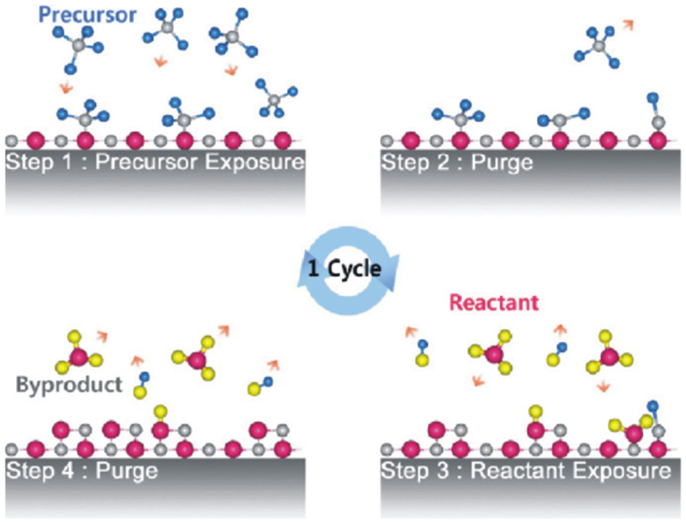
Figure 1. Schematic of ALD-growth process [reproduced with permission (Kim et al., 2009)]. Copyright 2009, Elsevier.
Atomic layer deposition is a modified form of Chemical Vapor Deposition (CVD) technique, which possesses angstrom level resolution, layer-by-layer growth of ultra-thin compound films on planar, and high aspect ratio micro- and nano-structures employed in various potential applications (Kim et al., 2009). It distinguishes from CVD in terms that the precursor material pulses are introduced in the reactor on to the substrate alternately, once at a time (Ponraj et al., 2013). The reactor is continuously purged with a commonly used inert gas such as nitrogen after each precursor pulse, which extracts all the reaction byproducts except those which are chemisorbed on the substrate. As a result, film growth proceeds through sequential surface reactions and enable self-limiting and self-controlled growth (Im et al., 2012). Owing to the self-controlled film growth, the extremely accurate film thickness in angstroms depends on the number of ALD-cycles (Riihelä et al., 1996). Another important consequence of self-controlled ALD-growth is that complex shaped high aspect ratio structures are uniformly coated over large-area substrates (George, 2010; Wang et al., 2014). ALD-Al2O3 is employed to uniformly coat silica spheres in synthetic opals (Sechrist et al., 2006). The wavelength of photonic crystals was investigated to shift progressively to longer wavelengths as a function of filled opal volume fraction by Al2O3 with pinhole defect free characteristics (Sechrist et al., 2006). This is worth emphasizing that films grown by ALD exhibit high density (Saleem et al., 2012b, 2013c, 2014d) e.g., the measured hydrogen contents in ALD-grown TiO2 (Ritala and Leskelä, 1993; Ritala et al., 1993) films are of lowest compared to those prepared by other techniques (Bennett et al., 1989). The high density consequently verifies, relative low concentrations of penetrated H2O molecules into ALD-grown films (Saleem et al., 2012b, 2013c, 2014d).
Typically, ALD-growth proceeds in slow fashion and produces sub-monolayer per cycle, which is a drawback of ALD technology. On the other hand, slow growth rates facilitate several high-tech processes as advantage and are paramount to ensure uniform high quality and pinhole defect free films over large areas. Since the origin of ALD technology is to deposit epitaxial layers on semiconductor substrates and were known as Atomic Layer Epitaxy (ALE) (Pimbley and Lu, 1985; Goodman and Pessa, 1986; Ide et al., 1988; Gong et al., 1990; Yu, 1993; Bedair, 1994), which demands thin dielectric gate oxide films (barrier layers) to control leakage current at minimum film thickness (Puurunen, 2005). Furthermore, in photonics high quality and dense thin films are of significant importance to confine propagating modes via lithographically fabricated nano-structured topographies (Riyanto et al., 2012). ALD-growth on such nano-structures proceeds as an independent process in order to mitigate any dimensional inaccuracies (Saleem et al., 2011a). Such nano-structural inaccuracies are possibly be adjusted by the thickness of ALD-growth as a function of number of ALD controlled cycles to deposit films of the order of Å.
2. Characteristics of ALD Films for the Fabrication of Nanophotonic Structures
Nanophotonic structures consist of periodic alternation of refractive index as high-low-high-low contrast that can change the state of polarization, amplitude, or phase of an incident light (Knop, 1978). The waveguide layer confines, propagates, and emerges the light as narrow spectral peaks by resonance of light modes within the structure. ALD-coated thin films play a significant role in the fabrication of nanophotonic structures to provide the following:
i. Excellent conformality of high aspect ratio nano-structures.
ii. Excellent step coverage uniformity and thickness control over large scale smooth surfaces.
iii. Low temperature growth, in particular on polymer materials below their glass transition temperatures as well as to deposit optical materials in amorphous phase.
iv. Reasonably good precursor material properties with minimum damage to substrate materials.
v. Self-saturative growth when the surface binding sites are filled and/or deposited film thickness is highly reproducible after each ALD-cycle.
2.1. Low Temperature ALD-Growth
One of the important feature of ALD is to grow high quality thin films at low growth temperatures 50–250°C (Triani et al., 2009; Im et al., 2012). Precursor molecules are thermally activated to react on the substrate surface and chemisorbed. Low temperature ALD-growth is extremely important for heat-sensitive materials such as polymers, biomaterials, and heat-sensitive structures: self-assembly of molecules, self-rolled microtubes with ultra-thin wall thickness (Purniawan et al., 2010; Im et al., 2012). TiO2 films at 80°C are deposited on plasma-treated polycarbonate substrate, which shows enhanced adhesion to ALD-coated films (Latella et al., 2007). Uniformly smooth thin amorphous ALD-TiO2 films possessing high refractive index are coated on replicated nano-structures on various polymer substrates such as polycarbonate, OrmoComp, Cyclic-Olefin-copolymer (COC) at low deposition temperature of 120°C and have been employed as Resonant Waveguide Gratings (RWGs) or Guided Mode Resonance Filters (GMRFs) (Saleem et al., 2011a, 2012a,d, 2013b, 2014a,c). ALD-TiO2 growth temperature has an effect on the film’s surface roughness, density, and refractive index owing to crystallization of TiO2 material to anatase phase. Increase in ALD-TiO2 growth temperature from 175 to 225°C led to increase surface roughness due to crystallization, consequently the fabricated films are porous with relatively low density and refractive index compared to amorphous films prepared at 125–150°C (Aarik et al., 2000), for further details see sections 3.1 and 3.2. A schematic representation of ALD-growth rate with growth temperature is shown in Figure 2 (Kääriäinen et al., 2013).
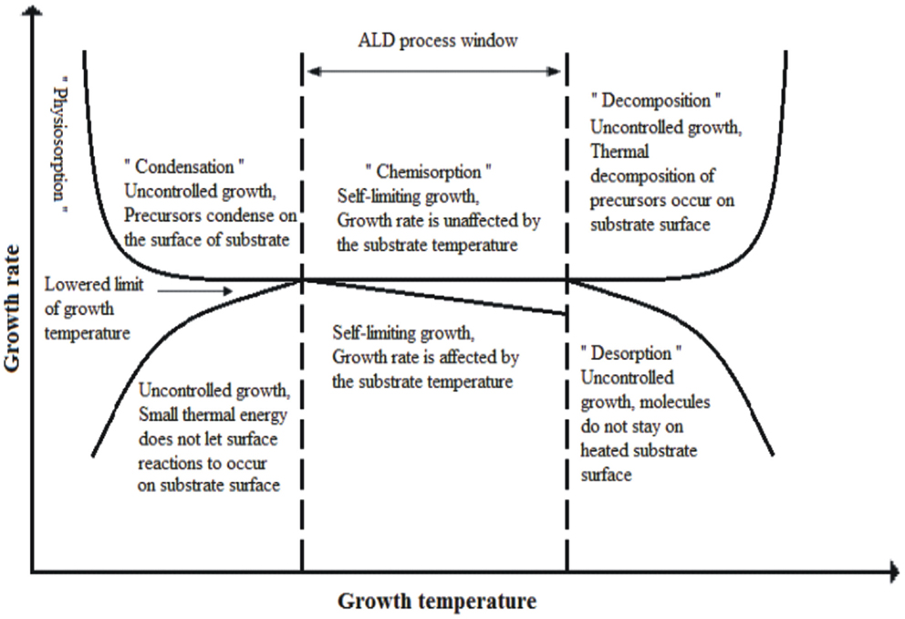
Figure 2. Schematic of ALD-growth process with temperature (Reproduced with permission © Picosun).
In order to explore the best operating regime of ALD one needs to adjust temperatures and growth rates. At high growth temperatures, the second precursor material decompose on the surface before reaction with first precursor and consequently deposit on the substrate by increasing the growth rate. Alternatively, the first stable precursor may desorb before reaction with second precursor, thereby decreasing the growth rate. On the other hand, if the temperature is too low, the precursor materials may desorb without a complete reaction or even condense a liquid or solid on the surface and results to increase in growth rate. Alternatively, precursor materials do not possess sufficient thermal energy to activate appropriate reactions and thus results in to lower the deposition rate than expected. Keeping all these parameters in consideration, a complete or partial monolayer of molecules can be deposited by selection of suitable temperature zone through ALD temperature window (Kääriäinen et al., 2013). Temperature variations during ALD-growth have significant influence on the surface roughness e.g., in infiltration of silica opals to fabricate TiO2 inverse opals with spherical size templates ranging from 200 to 440 nm in diameter show different roughness (King et al., 2005a). Atomic Force Microscopy (AFM) studies shows that TiO2 films yielded a root-mean-square (RMS) roughness of 0.2 nm at 100°C, 2.1 nm at 300°C, and 9.6 nm at 600°C, which shows that low temperature deposition is of much more significance for even filling and preparing extremely smooth interfaces (King et al., 2005a).
2.2. Self-Controlled Film Thickness and Material Composition
Atomic layer deposition technique is capable to deposit thin atomic films with precisely controlled thickness and free from occurrence of light losses in optical micro- and nano-devices resulted by thickness roughness (Vahala, 2003; Wang et al., 2012). Scanning electron microscopy (SEM) images in Figure 3A show the conformal growth of ALD-TiO2 films of various thicknesses of (0–120 nm) on Si triangular lattice of photonic crystals (PCs) (Graugnard et al., 2006). Transmission Electron Microscopy (TEM) images of four-bilayer nanolaminates of W/Al2O3 grown by ALD at temperature of 177°C are shown in Figure 3B (Sechrist et al., 2005). Each nanolaminate in the structure employing 111 ALD-cycles of Al2O3 and 32 to that of W, which are clearly shown in Figure 3B. Furthermore, it reveals that interfacial roughness is more prominent where Al2O3 nucleates on W and possesses less roughness at interfaces. Tungsten W grows on Al2O3 sites, which may results due to polycrystallinity of W nanolayer on Al2O3. More often, the ALD film growth is a fraction of one monolayer and has higher film density to those of films deposited by other techniques without pinhole defects (Carcia et al., 2009; Saleem et al., 2012b, 2013c).
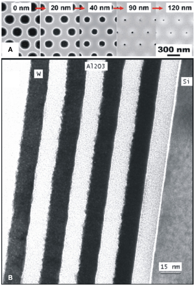
Figure 3. (A) SEM images of top view of Si triangular lattice of photonic crystals coated by various thicknesses (0–120 nm) of ALD-TiO2 films [reproduced with permission (Graugnard et al., 2006)]. Copyright 2006, American Institute of Physics. (B) TEM image of a four-bilayer ALD-W/Al2O3 nanolaminate structure grown at 177°C. ALD-Al2O3 was grown by 111 ALD-cycles and 32 ALD-cycles were used for W-nanolaminate [reproduced with permission (Sechrist et al., 2005)]. Copyright 2005, American Chemical Society.
2.3. Conformal Growth for 2D and 3D Structures
Atomic layer deposition is a unique technique relies on the sequential self-terminating surface saturating reactions between gas-phase precursor molecules and a solid surface. Owing to the self-limiting reactions, it gives better control on thickness, conformality, film quality and uniformity, and large-area coverage of high aspect ratio nano-structures, 3D complex structures such as PC, opals, nanopores, nanowires, and nanotubes (King et al., 2005b; Knez et al., 2007). Figure 4A shows the cross-sectional views of SEM images of ZnS:Mn and TiO2 infiltrated opals and inverted structures into silica opal templates. Figures 4B,C show the TiO2/SiO2 opals and TiO2 inverse opals where the growth in small central void space is precisely controlled by self-limiting nature of ALD, which enables accurately controlled deposition on complex geometries (King et al., 2005b). Figures 4D,E show a multi-layered PC structure using TiO2/ZnS:Mn/TiO2 in order to combine the luminescent properties of ZnS:Mn to that of higher refractive index of TiO2. The structure is fabricated with 10 nm of ZnS:Mn in a sintered opal followed by TiO2 deposition in remaining volume to fill. An Ion-mill is used to expose SiO2 opal and etch by HF to form an inverse opal, which is subsequently infiltrated by 10 nm of high refractive index ALD-TiO2 layer (King et al., 2005b).
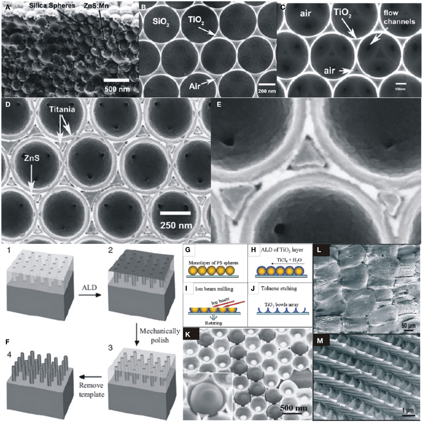
Figure 4. (A) SEM images of cross-sectional view of ZnS:Mn and TiO2 infiltrated opals and inverse opals into SiO2 opal templates. (B,C) SEM images of TiO2/SiO2 and TiO2 inverse opal. (D,E) Multi-layered PC structure of TiO2/ZnS:Mn/TiO2 into SiO2 opal template [reproduced with permission (King et al., 2005b)]. Copyright 2004, Elsevier. (F) Schematic fabrication of TiO2 nanotube arrays on Si substrate; (i) preparation of nanoporous Al-template by anodization of Al film, (ii) ALD-TiO2 deposited on Al-template, (iii) surface layer removal of TiO2, and (iv) chemical etching of Al-template to reveal dense, aligned, and uniform array of TiO2 nanotubes [reproduced with permission (Sander et al., 2004)]. Copyright 2004, Wiley. (G–J) Schematic of TiO2 nanobowls preparation. (K) Polystyrene (PS) spheres staying on a TiO2 nanobowls. The inset shows a PS sphere of 450 nm in size inside a TiO2 nanobowl [reproduced with permission (Wang et al., 2004)]. Copyright 2004, American Chemical Society. (L,M) SEM images of alumina replicas of butterfly wing scale on Si substrate after removal of butterfly template [reproduced with permission (Huang et al., 2006)]. Copyright 2006, American Chemical Society.
Uniform arrays of dense and aligned TiO2 nanotubes are fabricated by employing ALD on nanoporous Al2O3 on Si substrate as shown in Figure 4F (Sander et al., 2004). The catalytic properties of such TiO2 nanomembranes have been demonstrated by (Kemell et al., 2007). Wang et al. (2004) patterned self-assembled monolayer of hexagonally arranged polystyrene and SiO2 nanospheres. ALD-TiO2 and Al2O3 films are deposited on the substrate. TiO2 surface layer was removed by ion beam followed by removal of polystyrene beads to form a micrometer-scaled surface with TiO2 nanobowls as shown in Figures 4G–J. The structure of ALD-TiO2 nanobowls holding removable polystyrene nanospheres of size 450 nm are shown in Figure 4K. Such uniformly fabricated structures demonstrated the major advantages of ALD compared to other deposition methods such as CVD or PLD in terms of conformal growth on complex geometries. Highly complex morphology of butterfly wing’s structures are replicated after ALD coating (Huang et al., 2006) shown in Figures 4L,M. Modifications of such structures by ALD can improve their potential use as optical elements e.g., in holography. ALD-TiO2 was employed to tune the static photonic band of a 2D Si triangular lattice PC slab waveguide by nanoscale control of the dielectric contrast, propagation, and dispersion (Graugnard et al., 2006). This research group also reported the fabrication of 3D nano-structures through synthetic silica opals and holographically patterned polymeric templates to control PC band gap properties (Graugnard et al., 2006).
3. ALD Thin Films Optical Properties
The primary parameter to access the optical quality of a film is the complex refractive index with real part n and imaginary part k (extinction coefficient) and is related to the complex relative permittivity, εr = εr,r − iεr,i
where εr,r and εr,i represent the real and imaginary parts of εr, respectively. Equation (1) relates the dielectric properties of the materials with optical properties and depends on wavelength called dispersion. When light passes through a lossy material that absorbs or scatters light and loses its energy called attenuated light. Attenuation may occur due to several mechanisms such as generation of phonons (lattice waves), photogeneration, free carrier absorption, and scattering (Kasap and Capper, 2006). Equation (1) gives:
and
where the optical constants n and k can be determined from the reflectance of thin films for a specified polarization and angle of incidence of light. For normal incidence, the reflection coefficient r is given as:
Reflectance R is given as:
Larger values of k results in strong absorption and leads to reflectance almost unity. As a result light is reflected and any light in the medium is highly attenuated. In general, optical filter demands k(λ) below 10−4 with corresponding optical losses well below 1 dB/cm. In most optical thin films, the material selection requires amorphous (to avoid losses due to grain boundaries), isotropic, without birefringence and scattering losses below 10−4 (Martinu et al., 2014).
Figures 5A,B show the transmittance of ALD-TiO2 as deposited amorphous films of thickness ~200 nm on fused silica substrate with SEM image and heat treated ALD-TiO2 films in crystalline (anatase phase) with corresponding SEM image, respectively (Saleem et al., 2013a). Kumar et al. (2009) demonstrated the optical properties of thin Al2O3 films grown by ALD in the spectral range of 400–1800 nm and retrieved optical constants from reflection spectra using Sellmeier’s formula with mean square error values of 0.0006 and 0.0070 on silicon and soda lime glass substrates, respectively.
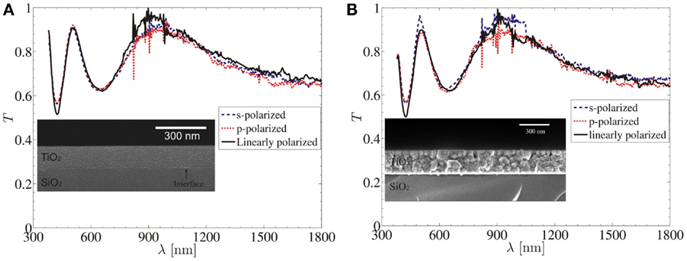
Figure 5. (A) Transmittance (T) of ALD-TiO2 as deposited film of thickness ~200 nm on fused silica substrate with inset of SEM image. (B) Transmittance (T) of ALD-TiO2 heat treated film (crystalline phase-anatase) of thickness ~200 nm on fused silica substrate with inset of SEM image [reproduced with permission (Saleem et al., 2013a)]. Copyright 2013, Optical Society of America.
3.1. Effect of ALD-Growth Temperature on Crystal Structure and Optical Scattering Losses
ALD-TiO2 films grow at 100–140°C exhibit amorphous phase while containing chlorine contaminations, which decreases significantly with increase in growth temperature. The composition of TiO2 films in terms of Ti/O ratio has a weak dependence on the growth temperature. The films grow at higher temperatures at 165–350°C possess polycrystalline anatase phase where preferential orientation of crystallites occur while the films at 400°C contained rutile phase. The scattering losses due to crystalline phases was attributed and characterized quantitatively by the half width of {220} and {440} reflections of Reflection High Energy Electron Diffraction (RHEED) patterns (Aarik et al., 1997a). A significantly perfect preferential orientation of crystallites results in a relatively smaller RHEED half widths, which predominantly occurred around 300°C for anatase phase while no preferential orientation at 400°C (rutile phase) appears (Aarik et al., 1997a). Furthermore, films with non-preferential orientation characteristics at growth temperature 400°C have significant absorption in transmission at 400–900 nm wavelength ranges and dominate scattering losses owing to low packing density and consequent surface roughness. The polycrystalline films absorption may also be attributing to the crystallites’ surfaces and/or grain interfaces.
3.2. Effect of ALD-Growth Temperature on Density and Refractive Index
The refractive index of the films grown at 300°C is higher than that the films grown at 100 and 400°C. This is attributed to a decrease in the scattering losses due to preferential orientation of crystallites (Aarik et al., 1997a). Unlike the anatase films, no preferential orientation occurs in rutile films at 400°C with substantial void contents between the crystallites, which result in decrease of packing density (Aarik et al., 1997a). This fact described a linear increase in refractive index with increase in film’s packing density (Ottermann and Bange, 1996) and a decrease in orientation scattering and surface roughness (Aarik et al., 1995). Similarly, Groner et al. (2004) demonstrated that the density of ALD-Al2O3 films decreases with decreasing growth temperature and estimated average densities ranged from 3.0 g/cm3 at 177°C to 2.5 g/cm3. ALD-Al2O3 film densities have been calculated by (Ott et al., 1997) using the Lorentz–Lorenz relationship based on refractive index. Groner et al. (2004) demonstrated that the refractive index of Al2O3 films decreases slightly with decreasing growth temperature with a reported refractive index n ≈ 1.67 at growth temperature 300–500°C. Other studies investigated that decrease in refractive index is caused by a density decrease with a rise in impurity levels at low growth temperatures (Kukli et al., 1997).
3.3. Effect of ALD-Growth Conditions on Physical Properties of Films
The polycrystalline phases (rutile/TiO2-II) observed at a film thickness as minimum as 3 nm at temperature 375–550°C using TiCl4 and H2O as precursor materials (Aarik et al., 1997b). The crystal structure is controlled by the pressure of H2O precursor. Films grown at low H2O pressure possesses TiO2-II phase while high H2O pressures are favorable and result in rutile phase. Such phase formation is influenced by the H2O dose on the hydroxyl surface groups or on the abundance of H2O in gas-phase. In addition, the structure depends on the film thickness. A pure TiO2-II phase appears below a critical thickness tc while rutile phase appeared at thickness above tc. Both structures co-exist at a thickness range of 150–180 nm and tc depends on the precursor pressures and subsequent purge times. Critical thickness tc reduces abruptly with short purge times while growth rate increase with decreasing purge times. This is attributed to overlapping of the reactant pulses and increase gas-phase reaction on the surface. The growth rate varies slowly with precursor doses while tc depends on both precursor doses (Aarik et al., 1997b).
ALD-Al2O3 growth has been studied more extensively than any other ALD system (George et al., 1996). Typical Trimethylaluminum (TMA) and H2O are used for the growth of ALD-Al2O3 as precursor materials. Groner et al. (2004) demonstrated maximum achievable growth rate ~1.33 Å/cycle of Al2O3 at 100 and 125°C, which is explained by essentially required thermal activation energy at lower temperatures and decreasing Al–OH and Al–CH3 surface coverage at higher temperatures (Ott et al., 1997). Growth rate depends on necessary surface species and subsequent reaction kinetics. At lower temperatures, the surface coverage becomes high, which dictates slow reaction kinetics while low surface coverage results due to rapid reaction kinetics at higher temperatures (Ott et al., 1997).
4. ALD-Growth in Nanophotonic Structures
4.1. ALD-Growth in Resonant Waveguide Gratings
4.1.1. Resonance anomalies and origination of RWG
Briefly describing the history of RWGs, when Wood in 1902 observed sharp spectral variations in the intensity of a metallic grating for TM-polarized light (electric field vector is perpendicular to grating lines), which he named anomalies (Wood, 1902). A theoretical explanation of these anomalies was given by Rayleigh in 1907 as one spectral order appearing at grazing incidence and occurred at a particular wavelength called Rayleigh wavelength and found close to Wood anomalies (Hessel and Oliner, 1965). Thereby, anomalies were categorized as Rayleigh and Resonance, which both were used for filtering applications. The employment of such anomalies of grating structures in dielectric materials referred to the term: RWGs or GMRFs (Saarinen et al., 2005). A diffraction grating consists of a periodic modulation of refractive index and guided mode resonance phenomena occurs when diffracted light from a diffraction grating couples with a leaky waveguide mode and satisfying phase-matching conditions, which results in a narrow linewidth peak at a particular wavelength that depends on a selectable range of optical parameters (Avrutskii et al., 1985). In this section, we briefly discuss the role of ALD-grown thin films in the development of RWGs.
4.1.2. Structure of a RWG
The structure of a RWG is shown in Figure 6A, which consists of a substrate with refractive index n3, an integrated diffraction grating with refractive index distribution n2(x) along x-direction and a medium from where light is incident (usually air) with refractive index n1. Figure 6A shows the direction of various propagating diffraction orders and can be simply calculated from the Eq. (6) (Saleem, 2012)
where d is grating period, λ is wavelength of incident light, θ1 is incident angle, m = 0, ± 1, ± 2, ± 3, … is the index of diffraction order, n1 and n2 are the refractive indices before and after the air-dielectric interface.
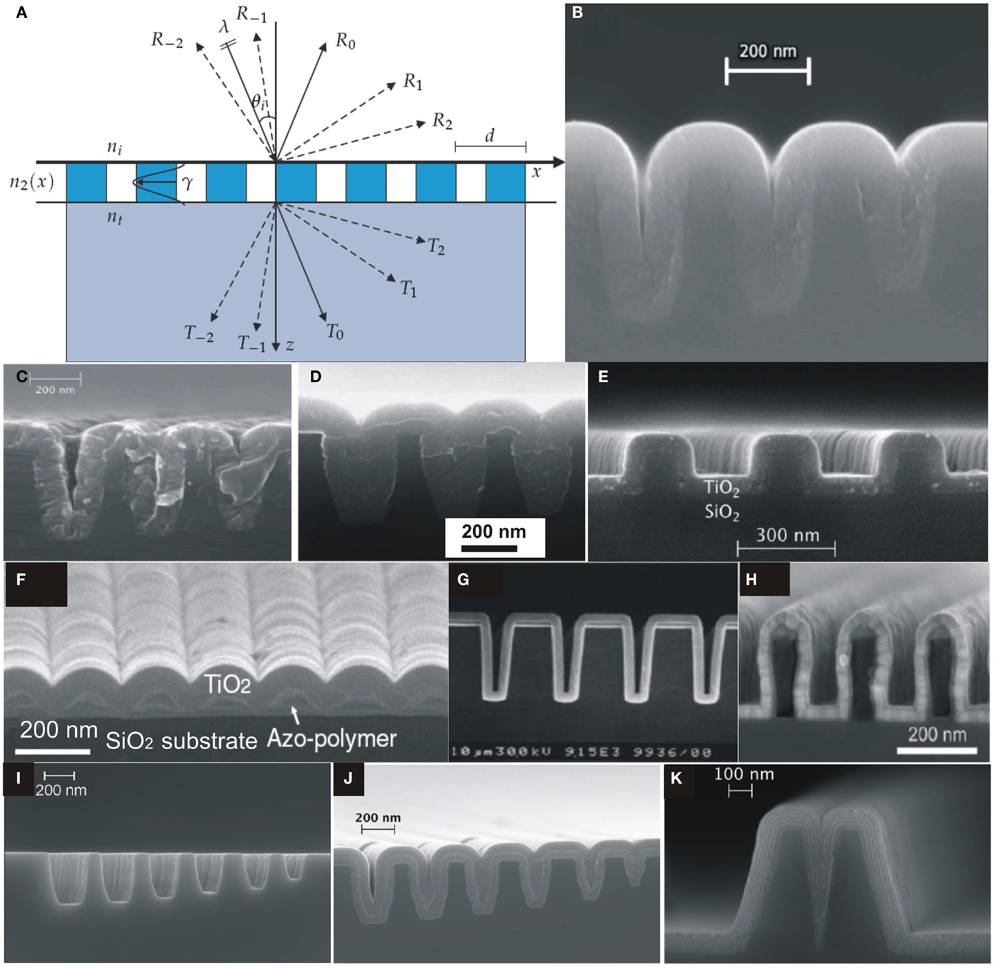
Figure 6. (A) A schematic illustration of resonant waveguide grating with forward and backward diffraction [reproduced with permission (Saleem, 2012)]. Copyright 2012, University of Eastern Finland. (B) SEM image of silicon slot structure coated by ALD-TiO2 amorphous layer at 120°C. ALD-grown amorphous layer of TiO2 on silicon slot structure [reproduced with permission (Alasaarela et al., 2010)]. Copyright 2010, Optical Society of America. (C) Without and (D) with intermediate Al2O3 layer [reproduced with permission (Alasaarela et al., 2010)]. Copyright 2010, Optical Society of America. (E) SEM image of TiO2 film on a silicon binary grating [reproduced with permission (Alasaarela et al., 2010)]. Copyright 2010, Optical Society of America. (F) SEM image of TiO2-coated sinusoidal profile of Azo-polymer on a glass substrate [reproduced with permission (Alasaarela et al., 2011b)]. Copyright 2011, Optical Society of America. (G) Cross-sectional view of SEM image of 300 nm ALD-grown Al2O3 film on Si wafer with trench structure [reproduced with permission (Ritala et al., 1999)]. Copyright 1999, WILEY-VCH Verlag GmbH. (H) SEM image of an overcoated polymer grating [reproduced with permission (Weber et al., 2012b)]. Copyright 2012, Elsevier. (I–K) Si-slot waveguide structures, filling by ALD-TiO2/Al2O3 film and filling by nanolamintes of ALD-TiO2/Al2O3, respectively [reproduced with permission (Säynätjoki et al., 2011)]. Copyright 2011, Optical Society of America.
4.1.3. ALD-growth in corrugated structures
Resonant waveguide gratings have been extensively studied since last couple of decades and several researchers fabricated RWG structures on various substrates employing ALD films to investigate their waveguiding properties, propagation losses, and fine tune the optical spectra (Alasaarela et al., 2010, 2011b; Saleem et al., 2011a, 2012a,d, 2013a,b, 2014a,c,d; Saleem, 2012). The fabrication of silicon photonic nano-structures is established about a decade using state-of-the-art 198 or 248 nm deep UV-lithographic techniques, which limit the structure size around 100 or 160 nm, respectively. For Si-slot waveguides, the achieved feature size was below 100 nm by partial filling with ALD-grown materials as well as to reduce the propagation losses (Alasaarela et al., 2009, 2011a; Säynätjoki et al., 2011; Karvonen et al., 2014). Figure 6B shows cross-section view of SEM image of a Si-slot waveguide coated by amorphous TiO2 film with a smooth surface showing peak-to-peak surface roughness <0.4 nm over an AFM measured area of 1 × 1 μm (Alasaarela et al., 2010).
Polycrystalline ALD-TiO2 films grown at 350°C exhibit propagation losses due to grain boundaries that can be minimized by depositing an intermediate ALD-grown layer of Al2O3 as shown in Figures 6B,C. As an example of conformal ALD-growth, RWG structure of a binary grating profile in fused silica substrate is coated by amorphous film of TiO2 as shown in Figure 6D. Figures 6E,F show SEM images of TiO2 films on a silicon binary grating and a sinusoidal grating profile fabricated on a hydrogen bonded polymer (Azobenzene Complex) that was spin coated on a glass substrate, respectively. The grating pattern was written using circularly polarized light of 488 nm Ar+ laser source of 300 mW/cm2 intensity to expose polymer. The fabricated polymer grating profile was coated with conformal TiO2 thin film by ALD at 80°C to avoid thermal degradation (Alasaarela et al., 2011b). Likewise, Figures 6G,H show the ALD conformal growth of Al2O3 on high aspect ratio corrugated structures (Ritala et al., 1999; Weber et al., 2012a). In Figures 6I–K silicon slot waveguide patterns to be filled by ALD-grown materials and the subsequent filling by ALD-Al2O3 and ALD-TiO2 in nano slots are shown, respectively. Moreover, the slots are filled as to demonstrate extremely uniform nanolaminate structure of five layers with 10 nm of each ALD-Al2O3 and ALD-TiO2 with reduced propagation losses compared to crystalline ALD-TiO2 films (Alasaarela et al., 2011a).
4.1.4. Propagation loss reduction with ALD-coated titanium dioxide thin films
The optical field in the waveguide structures must be confined and guided through with minimum field loss owing to controlled sidewall surface roughness without leakage into substrate that has been accompanied through uniform surface coatings of high index material(s). Alasaarela et al. (2010, 2011a) have shown that such propagation losses due to surface roughness could be reduced by conformal coatings of ALD-TiO2 films for which a further reduction in losses was measured by increasing film thickness. This attributes to increase in an effective index of waveguide to strongly confine the propagating waveguide modes and a significant reduction in surface roughness. Table 1 illustrates the values of waveguide losses (in decibels per centimeter) with an increase in the thickness of TiO2 film. We recently studied, theoretically, the optical dispersion engineering properties of silicon-strip waveguides using ALD-TiO2 films as overlayer on nano-structures (Erdmanis et al., 2012).
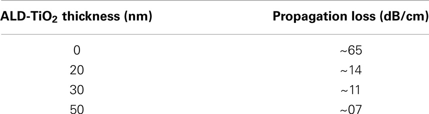
Table 1. Propagation loss values of silicon slot waveguides as a function of ALD-TiO2 film thickness.
4.1.5. ALD-growth in nanoreplicated corrugated profiles
Low temperature ALD-growth is of much more importance for polymeric substrate waveguides in applications for various bio-molecular sensors and RWGs (Triani et al., 2010; Magnusson et al., 2011). Nanoimprint technology was proposed by (Chou et al., 1997) in 1990s to fabricate replicated nano-structures. Transparent optical polymers have emerged as potential candidates in nanophotonic functional devices through replication in a wide variety of thermo-plastics (Herzig, 1997; Jaszewski et al., 1998; Mönkkönen et al., 2002; Liou and Chen, 2006) using replication tools of high replication fidelity and resolution to fabricate high aspect ratio structures (Pietarinen et al., 2007; Siitonen et al., 2007; Cui, 2008; Worgull, 2009). Recently, we have demonstrated conformal growth of ALD technique to fill various sub-wavelength RWG structures. A silicon master stamp was fabricated using hydrogen silsesquioxane (HSQ) resist without Reactive Ion Etching (RIE) process, which employed as to replicate sub-wavelength grating structures with different periods in thermoplastic polymers as shown in Figures 7A,D (Saleem et al., 2012c). The replicated grating structures in polycarbonate substrate with periods d = 425 and 368 nm are shown in Figures 7B,E and subsequently coated by thin amorphous films of ALD-TiO2 as shown in Figures 7C,H. Likewise, the replication of corrugated profiles in other polymers such as COC and OrmoComp and their overlayer ALD-TiO2 coatings are shown in Figures 7F,G and 7I,J, respectively. Figure 7K shows a replicated grating profile with period d = 540 nm, coated by 60 nm of ALD-TiO2 in applications of non-polarizing gratings (Saleem et al., 2012e). A high aspect ratio replicated structure followed by ALD-growth is depicted in Figure 7L. Saleem et al. (2011b) used such replicated polymeric gratings as athermal bio-molecular sensors within accuracy of a fraction of a nanometer. Furthermore, such sub-wavelength replicated grating structures in various polymers were compared in terms of their resonance peak stability, efficiency, full width half maximum (FWHM), ease of fabrication, and residual stresses for their use in potential applications (Saleem et al., 2013d). The interfacial adhesion of ALD-TiO2 films on polycarbonate substrate has been demonstrated by theoretical models based on experimental measurements (Triani et al., 2005; Latella et al., 2007).
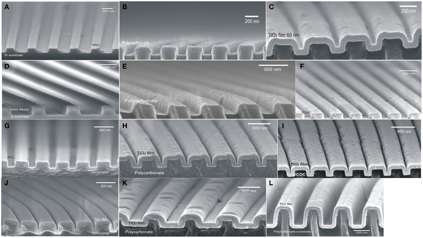
Figure 7. (A) Si-stamp of RWG with period d = 425 nm by HSQ resist without reactive ion etching. (B) Nanoimprinted profile of RWG in polycarbonate substrate by Si-Stamp of d = 425 nm. (C) Replicated grating profile coated by thin amorphous layer of ALD-TiO2. (D) Si-stamp of sub-wavelength RWG with period d = 325 nm by HSQ resist. (E) Replicated grating profile in polycarbonate. (F) Replicated grating profile in COC. (G) Replicated grating profile in OrmoComp. (H) Replicated grating profile in polycarbonate (d = 368 nm) coated by thin amorphous layer of ALD-TiO2. (I) Replicated grating profile in COC (d = 325 nm) coated by thin amorphous layer of ALD-TiO2. (J) Replicated grating profile in OrmoComp (d = 325 nm) coated by thin amorphous layer of ALD-TiO2. (K) Replicated grating profile in polycarbonate (d = 540 nm) coated by thin amorphous layer of ALD-TiO2 for non-polarizing properties. (L) Replicated grating profile in polycarbonate coated by thin amorphous layer of ALD-TiO2 showing high aspect ratio structure.
4.1.6. Effect of thickness of TiO2 films on replicated structures
A filtering design is recently proposed by Saleem et al. (2014b) with its real experimental demonstration to present the influence of ALD-TiO2 thickness layer on replicated nanostrcutures of RWGs. Polymeric rectangular grating profile with a ridge height h = 120 nm, period d = 425 nm, ridge width w = 268 nm, and duty cycle ff = w/d = 0.63 was covered by a thin dielectric TiO2 cover layer of thicknesses t = 60 and 75 nm, grown by ALD. The device was illuminated by a linearly polarized plane wave (TE polarization) from air at an angle of incidence θi = 20° and the specularly reflection was obtained at θo = 20°. Figure 8A shows the calculated field at TiO2 thicknesses of 60 and 75 nm and Figure 8B shows the simulated results by Fourier Modal Method (FMM) to predict spectral shift at (100%) maximum reflectance as a function of variation in waveguide thickness (TiO2 layer). A spectral shift of ~28 nm was calculated theoretically with an increase in ALD-TiO2 thickness by ~15 nm. Experimental measurements show specular reflectance resonance peaks at wavelengths 827 and 851 nm for t values of 60 and 75 nm, respectively as shown in Figure 8C. Such spectral shifts are attributed to increase in effective refractive index of waveguide, which result in an interaction of grating structure at longer wavelengths to originate resonance. Furthermore, simulated and experimentally measured results show slightly different spectral locations, which may arise due to surface roughness, true refractive indices of materials, structure linewidths, and slight variations in the periodicity after a number of fabrication steps (Saleem et al., 2011b).
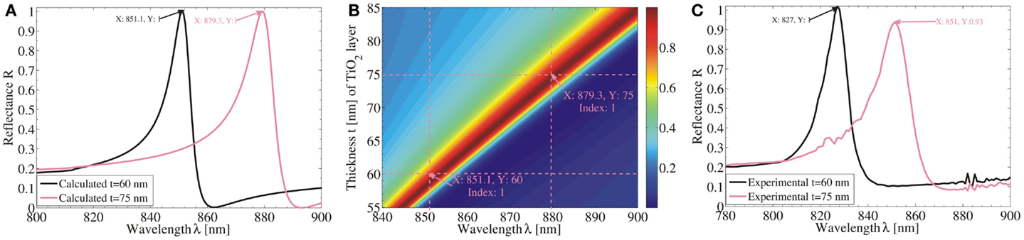
Figure 8. (A) Simulated spectra of replicated RWGs with ALD-TiO2 thickness of t = 60 and 75 nm. (B) Calculated field at t = 60 and 75 nm. (C) Experimentally measured spectra of RWGs with t = 60 and 75 nm.
4.2. ALD-Growth in Nanoplasmonics
Metallic nanoparticles have a number of valuable optical properties derived from their ability to collectively support the light-induced electronic oscillations to harness electromagnetic surface waves called, as surface plasmon polaritons (SPPs). SPPs are density fluctuations of conduction electrons in metals and propagate along metal surface with exponentially decaying evanescent field perpendicular to the metal-dielectric interface (Ritchie, 1957) and extend ~100–300 nm for visible light (Wei and Xu, 2014). SPPs have attractive features with metallic nanogaps, nanoholes, nanotips, nanoapertures, nanowires, or nanoparticles and concentrate optical field to nanoscale volumes and allow fundamental study of light–matter interactions at length scales, which were not accessible otherwise (Brongersma and Shalaev, 2010). Moreover, owing to sharp corners of engineered nano-structures, another important class of localized plasmon wave, which confines optical energy in a more tightly fashion at a relatively shorter decay length of 10–50 nm called, localized surface plasmons (LSPs) as shown in Figure 9A (Im et al., 2012) and likewise to SPPs confine maximum optical energy at metallic surfaces.
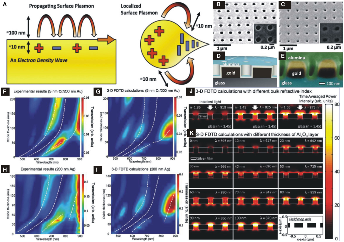
Figure 9. (A) Propagating SPPs and LSPs with evanescent field decaying length [reproduced with permission (Im et al., 2012)]. Copyright 2012, Materials Research Society. (B) SEM image of plasmonic structure with nanohole array on Au film with size 180 nm in diameter and 500 nm periodicity. (C) Same structure in (B) coated by ALD-Al2O3. (D) Schematic profile of ideal structure. (E) SEM image of cross-sectional view of nanoplasmonic structure. (F–I) Simulation results of maximum resonance and minimum transmission of Au- and Ag-nanohole array to show wavelength shift as a function of ALD-Al2O3 thickness. (J) Simulation results of FDTD to show maximum optical power distribution as a function of varying refractive index of surrounding region. (K) Simulation results of FDTD to show maximum optical power distribution as a function of varying ALD-Al2O3 thickness [(B–K) Reproduced with permission (Im et al., 2010)]. Copyright 2010, American Chemical Society.
Surface plasmon polaritons arise due to coupling between photons and conduction electrons, thereby, carrying higher momentum than free-space light. The momentum of light can be enhanced by illuminating a thin metallic film through a prism or strong grating coupling of patterned metallic surfaces (Raether, 1986).
4.2.1. ALD-Passive layer on metallic nanoplasmonic structures
ALD-grown nano-overlayers on metallic nanoplasmonic structures not only protect surface but also enhance the optical transmission. In most plasmonic devices operating at visible or infrared regimes, Ag or Au metals are used. At wavelengths below 600 nm, Ag has low ohmic losses, higher propagation lengths (low SPPs damping), higher sensitivity for biosensors, and are used in applications where a direct interface with biological molecules is not required, such as electrodes for plasmonic solar cells (Atwater and Polman, 2010). Silver Ag is used due to cost-effective solutions, better optical properties and relatively strong interfacial adhesion with glass substrates than Au (Ferry et al., 2008; Lindquist et al., 2008). Despite these advantages, Ag has lower chemical stability and readily oxidized in the air and shows a reduction in optical intensity in nanoplasmonic structures without passive layer (Im et al., 2010). While the Ag surfaces can be protected and improved in functionality by an overlayer of dielectric coating (~10–20 nm), which must be less than mean decay length of SPPs in order to annul from being absorption of SP field in thicker layers.
These ultra-thin barrier films must be dense, pinhole free, encapsulate the patterned structure entirely (Saleem et al., 2013c) and grown at a low deposition temperature to avoid degrading or oxidizing of underlying Ag film. Similarly, the use of silver nanoparticles coated by ~1 nm Al2O3 layer was investigated to preserve plasmon resonance peak after annealing at 500°C and have shown to degrade resonance peaks without Al2O3 layer even at annealing temperature of 200°C (Whitney et al., 2007). Likewise, Sung et al. (2008) showed enhanced thermal stability of Al2O3 coated silver nanoparticles against high power femtosecond laser. Self-assembly based plasmonic arrays tuned by minimum thickness of ALD fabricated (<20 nm) Au dots achieved enhanced visible light absorption per volume-equivalent thickness in applications including conversion of solar energy into electrical power (Hägglund et al., 2013). One of the possible reason of enhancing optical transmission is conformal and precisely uniform deposition of dielectric thin films on nano-structures is its predominance over rough topographies.
4.2.2. Tuning local refractive index of nanoplasmonic structures
The plasmonic resonance depends on the geometric parameters, incident angle, or wavelength, surrounding environmental conditions (dielectric constants), molecular layer bindings or adsorption, surface roughness, and the thickness of an overlayer on the metallic nano-structures. A change in any one of these parameters modify the resonance properties and ultimately shifts the resonance peak. Figure 9B shows an SEM image of nanohole array structure fabricated on Au (with 5 nm Cr adhesive layer) metallic film of 200 nm thickness by Focused Ion Beam with a period of 500 nm and hole diameter of 180 nm. A schematic of a nanoplasmonic structure coated by ALD-Al2O3 is shown in Figure 9D while top and cross-sectional views of SEM images of ALD-Al2O3 overlayer on metallic nanohole array are shown in Figures 9B,C and Figure 9E, respectively. Since, the ALD-Growth fills the nanoholes conformably and gives rise resonance spectral shifts as a result of tuning effective index seen by SPs, which is approximated by a simple model (Jung et al., 1998):
where nbulk and nfilm are the refractive indices of the surrounding bulk materials and thin deposited film, respectively, t is the thickness of the film and l is the decay length of SPs evanescent field perpendicular to the surface. It can be seen from Eq. (7) that as the thickness t of Al2O3 film increases, effective index increases from nbulk to nfilm, which results in a red-shift: here nbulk is air index and nfilm is Al2O3 index. Thereby, by varying t one can tune the resonance frequency of SPs precisely, since ALD grows films up to angstrom scale resolution. Furthermore, an increase in the t results in higher intensity that might be attributed to low SPs damping at relatively longer wavelengths as well as an increase in the periodicity of the structure reported by Przybilla et al. (2006). Furthermore, filling of nanoholes by ALD-Al2O3 not only results in higher effective index and reduction in waveguide-like attenuation of sub-wavelength structures for optical transmission enhancement but also encompasses index matching on both sides of the film. Thus, making an asymmetric peak to symmetric one with a transformation of (air–metal–glass) interfaces to (air–alumina–metal–glass) that boost optical transmission at a certain Al2O3 thickness where SPs wave sees almost a similar index above and below metallic structures (Krishnan et al., 2001).
4.2.3. Effect of Al2O3 thickness on spectral shifts
The effects of Al2O3 thickness on the spectral shifts have been investigated by theoretical calculations using 3D Finite Difference Time Domain (FDTD) simulations and compared with experimental results, not shown here [see Im et al. (2010)]. Figures 9F,G show a comparison of calculated results with ALD-Al2O3 deposition with a step of 6 and 10 nm on gold sample, respectively and white dashed lines depict resonance maxima and transmission minima. An increase in ALD-Al2O3 thickness not only results in red-shift but also increases transmission intensity by a factor of about 5 at certain thickness value. Likewise, Ag-nanohole arrays show the calculated results and their consistency with experimentally measured ones, as seen in Figures 9H,I.
3D FDTD simulations were carried out to validate the optical field distribution in each nanohole as a function of index matching on top and bottom sides of metallic films. In these simulations the bulk refractive index over nanohole arrays is varied from 1.35 to 1.55. Figure 9J shows that the maximum transmitted field intensity and output power occurs when the nbulk above and inside of each nanohole matches to that of the glass substrate with index 1.45 and Krishnan et al. (2001) demonstrated that under such symmetric conditions optical transmission enhances by a factor of 10 compared to asymmetric interfaces. Figure 9K shows FDTD calculated results of filed distributions in nanohole arrays for different values of Al2O3 overlayer by considering the refractive indices of glass and alumina 1.45 and 1.65, respectively. At symmetric condition one expects that the effective index seen by the SP waves approximately matches to that of substrate (glass) and maximum electromagnetic power distribution occurs at certain thickness value of t = 60–70 nm. Hence, ALD overlayer can tune and shift transmission spectrum in a precisely and controlled manner, which is of significant importance in biochemical sensing, surface plasmon resonance imaging (Chinowsky et al., 2004), biomimetic sensing, and membrane protein research.
5. Conclusion
Due to continuous device miniaturization, precise control of thin film growth is essential at the atomic level to fabricate nano-optical and semiconductor devices. To target such requirements, ALD methods have been developed for the growth of ultra-thin and highly conformal and uniform films. ALD is a vapor phase technique based on sequential and self-limiting growth on functional surfaces as well as on substrates with high aspect ratios after chemical reactions. The use of ALD deposited optical materials such as TiO2 and Al2O3 in nanophotonic devices are discussed.
Atomic layer deposition is capable of smooth and uniform deposition on a wide variety of organic and inorganic materials in a number of high-Tech applications including bio-molecular sensors, biomimetic sensing, membrane proteins, nanophotonic and microelectronic devices. ALD coatings can conformably fill the PC of metallic nanohole arrays that increases the extraordinary optical transmission of plasmonic structures and to reduce the feature size of the silicon waveguides and propagation losses. The increase in ALD-TiO2 thickness results in a further reduction in propagation losses in Si-slot waveguides and increase in transmission through plasmonic structures due to increase in effective index of the structures. The low deposition rate of ALD is extremely important to deposit high density, high quality, and uniform thin films in microelectronics industry as high-k gate oxide thin barrier layers as well as to propagate evanescent modes with relatively longer decay lengths in photonics. The low temperature growth enables and emerges ALD as a unique technique to deposit coatings on polymer substrates, temperature sensitive materials, and bio-molecular materials to avoid their degradation. ALD-growth on several substrates also promises to protect the underneath surfaces/structures from environmental effects due to extremely low penetration through high density and pinhole free films.
The future prospects of ALD are very promising. ALD should also play an integral role in new paradigms for optical materials in nanophotonics. The number of applications for ALD also continues to grow outside of the semiconductor arena. The future should see ALD continue to expand into new areas and find additional applications and challenges in demanding protective coatings, microelectromechanical systems, nanoelectronics, solar cells etc., that benefit from its precise thickness control and conformality.
Conflict of Interest Statement
The authors declare that the research was conducted in the absence of any commercial or financial relationships that could be construed as a potential conflict of interest.
Acknowledgments
Financial support from Strategic funding Initiative TAILOR of the University of Eastern Finland, Academy of Finland, Tekes (Finland), Higher Education Commission (HEC), USAID Center for Advance Studies, CES, NUST, (Pakistan) are greatly appreciated.
References
Aarik, J., Aidla, A., Kiisler, A.-A., Uustare, T., and Sammelselg, V. (1997a). Effect of crystal structure on optical properties of TiO2 films grown by atomic layer deposition. Thin Solid Films 305, 270–273. doi:10.1016/S0040-6090(97)00135-1
Aarik, J., Aidla, A., Sammelselg, V., and Uustare, T. (1997b). Effect of growth conditions on formation of TiO2-ii thin films in atomic layer deposition process. J. Cryst. Growth 181, 259–264. doi:10.1016/S0022-0248(97)00279-0
Pubmed Abstract | Pubmed Full Text | CrossRef Full Text | Google Scholar
Aarik, J., Aidla, A., Mändar, H., and Sammelselg, V. (2000). Anomalous effect of temperature on atomic layer deposition. J. Cryst. Growth 220, 531–537. doi:10.1016/S0022-0248(00)00897-6
Aarik, J., Aidla, A., Uustare, T., and Sammelselg, V. (1995). Morphology and structure of TiO2 thin films grown by atomic layer deposition. J. Cryst. Growth 148, 268–275. doi:10.3762/bjnano.5.7
Pubmed Abstract | Pubmed Full Text | CrossRef Full Text | Google Scholar
Alasaarela, T., Korn, D., Alloatti, L., Säynätjoki, A., Tervonen, A., Palmer, R., et al. (2011a). Reduced propagation loss in silicon strip and slot waveguides coated by atomic layer deposition. Opt. Express 19, 11529–11538. doi:10.1364/OE.19.011529
Pubmed Abstract | Pubmed Full Text | CrossRef Full Text | Google Scholar
Alasaarela, T., Zheng, D., Huang, L., Priimagi, A., Bai, B., Tervonen, A., et al. (2011b). Single-layer one-dimensional nonpolarizing guided-mode resonance filters under normal incidence. Opt. Lett. 36, 2411–2413. doi:10.1364/OL.36.002411
Pubmed Abstract | Pubmed Full Text | CrossRef Full Text | Google Scholar
Alasaarela, T., Saastamoinen, T., Hiltunen, J., Aäynätjoki, A., Tervonen, A., Stenberg, P., et al. (2010). Atomic layer deposited titanium dioxide and its application in resonant waveguide grating. Appl. Opt. 49, 4321–4325. doi:10.1364/AO.49.004321
Pubmed Abstract | Pubmed Full Text | CrossRef Full Text | Google Scholar
Alasaarela, T., Säynätjoki, A., Hakkarainen, T., and Honkanen, S. (2009). Feature size reduction of silicon slot waveguide by partial filling using atomic layer deposition. Opt. Eng. 48, 080502. doi:10.1117/1.3206731
Atwater, H. A., and Polman, A. (2010). Plasmonics for improved photovoltaic devices. Nat. Mater. 9, 205–213. doi:10.1038/nmat2629
Pubmed Abstract | Pubmed Full Text | CrossRef Full Text | Google Scholar
Avrutskii, D., Golubenko, G., Sychugov, V., and Tishchenko, A. (1985). Light reflection from the surface of a corrugated waveguide. Sov. Tech. Phys. Lett. 11, 401–402.
Bedair, S. (1994). Atomic layer epitaxy deposition processes. J. Vac. Sci. Technol. B12, 179. doi:10.1116/1.587179
Bennett, J. M., Pelletier, E., Albrand, G., Borgogno, J., Lazarides, B., Carniglia, C. K., et al. (1989). Comparison of the properties of titanium dioxide films prepared by various techniques. Appl. Opt. 28, 3303–3317. doi:10.1364/AO.28.003303
Pubmed Abstract | Pubmed Full Text | CrossRef Full Text | Google Scholar
Brongersma, M. L., and Shalaev, V. M. (2010). The case for plasmonics. Appl. Phys. 328, 440–441. doi:10.1126/science.1186905
Carcia, P., McLean, R., Groner, M., Dameron, A., and George, S. (2009). Gas diffusion ultrabarriers on polymer substrates using Al2O3 atomic layer deposition and SiN plasma-enhanced chemical vapor deposition. J. Appl. Phys. 106, 23533. doi:10.1063/1.3159639
Chinowsky, T. M., Mactutis, T., Fu, E., and Yager, P. (2004). Optical and electronic design for a high-performance surface plasmon resonance imager. SPIE Proc. 5261, 173–182. doi:10.1117/12.538536
Chou, S., Krauss, P., Zhang, W., Guo, L., and Zhuang, L. (1997). Sub-10 nm imprint lithography and application. J. Vac. Sci. Technol. B 15, 2897–2904. doi:10.1116/1.589752
Chung, C., Liao, M., and Lai, C. (2009). Effect of oxygen flow ratios and annealing temperatures on Raman and photoluminescence of titanium oxide thin films deposited by reactive magnetron sputtering. Thin Solid Films 518, 1415–1418. doi:10.1016/j.tsf.2009.09.076
Dobrowolski, J. A., Tikhonravov, A. V., Trubetskov, M. K., Sullivan, B. T., and Verly, P. G. (1996). Optimal single-band normal incidence antireflection coatings. Appl. Opt. 35, 644–658. doi:10.1364/AO.35.000644
Pubmed Abstract | Pubmed Full Text | CrossRef Full Text | Google Scholar
Erdmanis, M., Karvonen, L., Saleem, M. R., Ruoho, M., Pale, V., Tervonen, A., et al. (2012). Ald-assisted multiorder dispersion engineering of nanophotonic strip waveguides. J. Lightwave Technol. 30, 2488–2493. doi:10.1109/JLT.2012.2200235
Ferry, V. E., Sweatlock, L. A., Pacifici, D., and Atwater, H. A. (2008). Plasmonic nanostructure for efficient light coupling into solar cells. Nano Lett. 8, 4391–4397. doi:10.1021/nl8022548
Pubmed Abstract | Pubmed Full Text | CrossRef Full Text | Google Scholar
George, S., Ott, A., and Klaus, J. (1996). Surface chemistry for atomic layer growth. J. Phys. Chem. 100, 13121–13131. doi:10.1021/jp9536763
George, S. M. (2010). Atomic layer deposition: an overview. Chem. Rev. 110, 111–131. doi:10.1021/cr900056b
Gong, J., Jung, D., El-Masry, N., and Bedair, S. (1990). Atomic layer epitaxy of AlGaAs. J. Appl. Phys. 57, 400.
Goodman, C. H., and Pessa, M. V. (1986). Atomic layer epitaxy. J. Appl. Phys. 60, R65. doi:10.1063/1.337344
Graugnard, E., Gaillot, D. P., Dunham, S. N., Neff, C. W., Yamashita, T., and Summers, C. J. (2006). Photonic band tuning in two-dimensional photonic crystal slab waveguides by atomic layer deposition. Appl. Phys. Lett. 89, 181108. doi:10.1063/1.2360236
Groner, M., Fabreguette, F., Elam, J., and George, S. (2004). Low-temperature Al2O3 atomic layer growth. J. Chem. Mater. 16, 639–645. doi:10.1021/cm0304546
Hägglund, C., Zeltzer, G., Ruiz, R., Thomann, I., Lee, H.-B.-R., Brongersma, M. L., et al. (2013). Self-assembly based plasmonic arrays tuned by atomic layer deposition for extreme visible light absorption. Nano Lett. 13, 3352–3357. doi:10.1021/nl401641v
Pubmed Abstract | Pubmed Full Text | CrossRef Full Text | Google Scholar
Hessel, A., and Oliner, A. (1965). A new theory of wood’s anomalies on optical coatings. Appl. Opt. 4, 1275–1297. doi:10.1364/AO.4.001275
Huang, J., Wang, X., and Wang, Z. L. (2006). Controlled replication of butterfly wings for achieving tunable photonic properties. Nano Lett. 6, 2325–2331. doi:10.1021/nl061851t
Pubmed Abstract | Pubmed Full Text | CrossRef Full Text | Google Scholar
Huber, S., der Kruijs, R., Yakshin, A., and Zoethout, E. (2014). Subwavelength single layer absorption resonance antireflection coatings. Opt. Express 22, 490–497. doi:10.1364/OE.22.000490
Pubmed Abstract | Pubmed Full Text | CrossRef Full Text | Google Scholar
Ide, Y., McDermott, B., Hashemi, M., Bedair, S., and Goodhue, W. (1988). Sidewall growth by atomic layer epitaxy. J. Appl. Phys. 53, 2314.
Im, H., Lindquist, N. C., Lesuffleur, A., and Oh, S.-H. (2010). Atomic layer deposition of dielectric overlayers for enhancing the optical properties and chemical stability of plasmonic nanoholes. ACS Nano 4, 947–954. doi:10.1021/nn901842r
Pubmed Abstract | Pubmed Full Text | CrossRef Full Text | Google Scholar
Im, H., Wittenberg, N. J., Lindquist, N. C., and Oh, S.-H. (2012). Atomic layer deposition: a versatile technique for plasmonics and nanobiotechnology. J. Mater. Res. 27, 663–671. doi:10.1557/jmr.2011.434
Pubmed Abstract | Pubmed Full Text | CrossRef Full Text | Google Scholar
Jalaluddin, M., and Magnusson, R. (2013). Guided-mode resonant thermo-optic tunable filters. IEEE Photonics Technol. Lett. 25, 1412–1415. doi:10.1109/LPT.2013.2266272
Jaszewski, R., Schift, H., Gobrecht, J., and Smith, P. (1998). Hot embossing in polymers as a direct way to pattern resist. Microelectron. Eng. 4, 575–578. doi:10.1016/S0167-9317(98)00135-X
Jia, K., Zhang, D., and Ma, J. (2011). Sensitivity of guided mode resonance filter-based biosensor in visible and near infrared ranges. Sens. Actuators B Chem. 156, 194–197. doi:10.1016/j.snb.2011.04.013
Jung, L. S., Campbell, C. T., Chinowsky, T. M., Mar, M. N., and Yee, S. S. (1998). Quantitative interpretation of the response of surface plasmon resonance sensors to adsorbed films. Langmuir 14, 5636–5648. doi:10.1021/la971228b
Kääriäinen, T., Cameron, D., Kääriäinen, M.-L., and Sherman, A. (2013). Atomic Layer Deposition: Principles, Characteristics, and Nanotechnology Applications. Beverly, MA: Scrivener publishing, Wiley.
Karvonen, L., Säynätjoki, A., Roussey, M., Kuittinen, M., and Honkanen, S. (2014). Application of atomic layer deposition in nanophotonics. SPIE Proc. 8988, 89880Z–89881Z. doi:10.1364/OE.21.032417
Pubmed Abstract | Pubmed Full Text | CrossRef Full Text | Google Scholar
Kasap, S., and Capper, P. (eds) (2006). Handbook of Electronic and Photonic Materials. New York, NY: Springer.
Kemell, M., Pore, V., Tupala, J., Ritala, M., and Leskelä, M. (2007). Atomic layer deposition of nanostructured TiO2 photocatalysts via template approach. Chem. Mater. 19, 1816–1820. doi:10.1021/cm062576e
Kim, H., Lee, H.-B., and Maeng, W.-J. (2009). Applications of atomic layer deposition to nanofabrication and emerging nanodevices. Thin Solid Films 517, 2563–2580. doi:10.1016/j.tsf.2008.09.007
King, J. S., Graugnard, E., and Summers, C. J. (2005a). TiO2 inverse opals fabricated using low-temperature atomic layer deposition. Adv. Mater. 17, 1010–1013. doi:10.1002/adma.200400648
King, J., Heineman, D., Graugnard, E., and Summers, C. (2005b). Atomic layer deposition in porous structures: 3D photonic crystals. Appl. Surf. Sci. 244, 511–516. doi:10.1016/j.apsusc.2004.10.110
Knez, M., Nielsch, K., and Niinistö, L. (2007). Synthesis and surface engineering of complex nanostructures by atomic layer deposition. Adv. Mater. 19, 3425–3438. doi:10.1002/adma.200700079
Knop, K. (1978). Rigorous diffraction theory for transmission phase gratings with deep rectangular grooves. J. Opt. Soc. Am. 68, 1206–1210. doi:10.1364/AO.17.003598
Pubmed Abstract | Pubmed Full Text | CrossRef Full Text | Google Scholar
Krishnan, A., Thio, T., Kim, T., Lezec, H., Ebbesen, T., Wolff, P., et al. (2001). Evanescently coupled resonance in surface plasmon enhanced transmission. Opt. Commun. 200, 1–7. doi:10.1016/S0030-4018(01)01558-9
Kukli, K., Ritala, M., Leskelä, M., and Jokinen, J. (1997). Atomic layer epitaxy growth of aluminum oxide thin films from a novel Al(CH3)2Cl precursor and H2O. J. Vac. Sci. Technol. A 15, 2214–2218. doi:10.1116/1.580536
Kumar, P., Wiedmann, M. K., Winter, C. H., and Avrutsky, I. (2009). Optical properties of Al2O3 thin films grown by atomic layer deposition. Appl. Opt. 48, 5407–5412. doi:10.1364/AO.48.005407
Pubmed Abstract | Pubmed Full Text | CrossRef Full Text | Google Scholar
Latella, B., Triani, G., Zhang, Z., Short, K., Bartlett, J., and Ignat, M. (2007). Enhanced adhesion of atomic layer deposited titania on polycarbonate substrates. Thin Solid Films 515, 3138–3145. doi:10.1016/j.tsf.2006.08.022
Lindquist, N. C., Luhman, W. A., Oh, S.-H., and Holmes, R. J. (2008). Plasmonic nanocavity arrays for enhanced efficiency in organic photovoltaic cells. Appl. Phys. Lett. 93, 123308. doi:10.1063/1.2988287
Liou, A., and Chen, R. (2006). Injection molding of polymer micro- and sub-micron structures with high-aspect ratios. Int. J. Adv. Manuf. Technol. 28, 1097–1103. doi:10.1007/s00170-004-2455-2
Magnusson, R., Wowro, D., Zimmerman, S., and Ding, Y. (2011). Resonant photonic biosensors with polarization-based multiparametric discrimination in each channel. Sensors 11, 1476–1488. doi:10.3390/s110201476
Pubmed Abstract | Pubmed Full Text | CrossRef Full Text | Google Scholar
Martinu, L., Hichwa, B., and Klemberg-Sapieha, J. E. (2014). Advances in Optical Coatings Stimulated by the Development of Deposition Techniques and the Control of Ion Bombardment. Berlin: Springer, 36–45.
Mönkkönen, K., Hietala, J., Pääkkönen, P., Kaikuranta, T., Pakkanen, T., and Jääskeläinen, T. (2002). Replication of sub-micron features using amorphous thermoplastics. Polym. Eng. Sci. 42, 1600–1608. doi:10.1002/pen.11055
Ott, A., Klaus, J., George, S. M., and Johnson, J. M. (1997). Al2O3 thin film growth on si (100) using binary reaction sequence chemistry. Thin Solid Films 292, 135–144. doi:10.1016/S0040-6090(96)08934-1
Ottermann, C., and Bange, K. (1996). Correlation between the density of TiO2 films and their properties. Thin Solid Films 286, 32–34. doi:10.1016/S0040-6090(96)08848-7
Pietarinen, J., Siitonen, S., Immonen, J., Suvanto, M., Kuittinen, M., Mönkkönen, K., et al. (2007). Transparent thermoplastics: replication of diffractive optical elements using micro-injection molding. Opt. Mater. 30, 285–291. doi:10.1016/j.optmat.2006.11.046
Pimbley, J., and Lu, T.-M. (1985). Two-dimensional atomic correlations of epitaxial layers. J. Appl. Phys. 57, 4583. doi:10.1063/1.335364
Ponraj, J. S., Attolini, G., and Bosi, M. (2013). Review on atomic layer deposition and applications of oxide thin films. Crit. Rev. Solid State Mater. Sci. 38, 203–233. doi:10.1080/10408436.2012.736886
Przybilla, F., Degiron, A., Laluet, J.-Y., Genet, C., and Ebbesen, T. (2006). Optical transmission in perforated noble and transition metal films. J. Opt. 8, 458–456. doi:10.1088/1464-4258/8/5/015
Purniawan, A., French, P., Pandraud, G., and Sarro, P. (2010). TiO2 ald nanolayer as evanescent waveguide for biomedical sensor applications. Procedia Eng. 5, 1131–1135. doi:10.1016/j.proeng.2010.09.310
Puurunen, R. L. (2005). Surface chemistry of atomic layer deposition: a case study for the trimethylaluminum/water process. J. Appl. Phys. 97, 121301. doi:10.1063/1.1940727
Raether, H. (1986). Surface Plasmons on Smooth and Rough Surfaces and on Gratings. Berlin: Springer-Verlag.
Riihelä, D., Ritala, M., Matero, R., and Leskelä, M. (1996). Introducing atomic layer epitaxy for the deposition of optical thin films. Thin Solid Films 289, 250–255. doi:10.1016/S0040-6090(96)08890-6
Ritala, M., and Leskelä, M. (1993). Growth of titanium dioxide thin films by atomic layer epitaxy. Thin Solid Films 225, 288–295. doi:10.1016/0040-6090(93)90172-L
Ritala, M., Leskelä, M., Dekker, J.-P., Mutsaers, C., Soininen, P. J., and Skarp, J. (1999). Perfectly conformal TiN and Al2O3 films deposited by atomic layer deposition. Chem. Vap. Deposition 5, 7–9. doi:10.1002/(SICI)1521-3862(199901)5:1<7::AID-CVDE7>3.0.CO;2-J
Ritala, M., Leskelä, M., Niinistö, L., and Haussalo, P. (1993). Titanium isopropoxide as a precursor in atomic layer epitaxy of titanium dioxide thin films. Chem. Mater. 5, 1174–1181. doi:10.1021/cm00032a023
Ritchie, R. (1957). Plasma losses by fast electron in thin films. Phys. Rev. 106, 874–881. doi:10.1103/PhysRev.106.874
Riyanto, E., Rijanto, E., and Prawara, B. (2012). A review of atomic layer deposition for nanoscale devices. Mechatron. Electrical Power Vehicular Technol 3, 65–72. doi:10.14203/j.mev.2012.v3.65-72
Saarinen, J., Noponen, E., and Turunen, J. (2005). Guided mode resonance filters of finite aperture. J. Opt. Eng. 34, 2560–2566. doi:10.1117/12.208079
Pubmed Abstract | Pubmed Full Text | CrossRef Full Text | Google Scholar
Saleem, M., Khan, M., Khan, Z., Stenberg, P., Alasaarela, T., Honkanen, S., et al. (2011a). Thermal behavior of waveguide gratings. SPIE Proc. 8069, 80690A–80691A. doi:10.1117/12.885708
Saleem, M., Stenberg, P., Alasaarela, T., Silfsten, P., Khan, M., Honkanen, S., et al. (2011b). Towards athermal organic-inorganic guided mode resonance filters. Opt. Express 19, 24241–24251. doi:10.1364/OE.19.024241
Pubmed Abstract | Pubmed Full Text | CrossRef Full Text | Google Scholar
Saleem, M. R. (2012). Resonant Waveguide Gratings by Replication and Atomic Layer Deposition. Ph.D., thesis, Department of Physics and Mathematics, University of Eastern Finland, Joensuu.
Saleem, M. R., Ali, R., Honkanen, S., and Turunen, J. (2014a). Determination of thermo-optic properties of atomic layer deposited thin TiO2 films for athermal resonant waveguide gratings by spectroscopic ellipsometry. SPIE Proc. 9130, 9130A–9131A. doi:10.1117/12.2052299
Saleem, M. R., Ali, R., Honkanen, S., and Turunen, J. (2014b). Effect of waveguide thickness layer on spectral resonance of a guided mode resonance filter. IEEE (IBCAST) Proc. 14197105, 39–43. doi:10.1109/IBCAST.2014.6778117
Saleem, M. R., Honkanen, S., and Turunen, J. (2014c). Mode-splitting of a non-polarizing guided mode resonance filter by substrate overetching effect. SPIE Proc. 8974, 897417–897411. doi:10.1117/12.2038116
Saleem, M. R., Honkanen, S., and Turunen, J. (2014d). Thermal properties of TiO2 films fabricated by atomic layer deposition. IOP Conf. Ser. Mater. Sci. Eng. 60, 012008. doi:10.1088/1757-899X/60/1/012008
Saleem, M. R., Honkanen, S., and Turunen, J. (2012a). Partially athermalized waveguide gratings. SPIE Proc. 8428, 842817–842811. doi:10.1117/12.922070
Saleem, M., Honkanen, S., and Turunen, J. (2012b). Thermal properties of TiO2 films grown by atomic layer deposition. Thin Solid Films 520, 5442–5446. doi:10.1016/j.tsf.2012.04.008
Saleem, M., Stenberg, P., Khan, M., Khan, Z., Honkanen, S., and Turunen, J. (2012c). Hydrogen silsesquioxane resist stamp for replication of nanophotonic components in polymers. J. Micro Nanolithogr. MEMS MOEMS 11, 013007. doi:10.1117/1.JMM.11.1.013007
Saleem, M., Stenberg, P., Khan, M., Khan, Z., Honkanen, S., and Turunen, J. (2012d). HSQ resist for replication stamp in polymers. SPIE Proc. 8249, 82490G. doi:10.1117/12.907862
Saleem, M., Zheng, D., Bai, B., Kuittinen, P. S. M., Honkanen, S., and Turunen, J. (2012e). Replicable one-dimensional non-polarizing guided mode resonance gratings under normal incidence. Opt. Express 20, 16974–16980. doi:10.1364/OE.21.000345
Pubmed Abstract | Pubmed Full Text | CrossRef Full Text | Google Scholar
Saleem, M. R., Honkanen, S., and Turunen, J. (2013a). Effect of substrate overetching and heat treatment of titanium oxide waveguide gratings and thin films on their optical properties. Appl. Opt. 52, 422–432. doi:10.1364/AO.52.000422
Pubmed Abstract | Pubmed Full Text | CrossRef Full Text | Google Scholar
Saleem, M. R., Honkanen, S., and Turunen, J. (2013b). Non-polarizing single layer inorganic and double layer organic-inorganic one-dimensional guided mode resonance filters. SPIE Proc. 8613, 86130C–86131C. doi:10.1117/12.2001692
Saleem, M., Ali, R., Honkanen, S., and Turunen, J. (2013c). Thermal properties of thin Al2O3 films and their barrier layer effect on thermo-optic properties of TiO2 films grown by atomic layer deposition. Thin Solid Films 542, 257–262. doi:10.1016/j.tsf.2013.06.030
Saleem, M., Honkanen, S., and Turunen, J. (2013d). Thermo-optic coefficient of ormocomp and comparison of polymer materials in athermal replicated subwavelength resonant waveguide gratings. Opt. Commun. 288, 56–65. doi:10.1016/j.optcom.2012.09.061
Sander, M., Côté, M., Gu, W., Kile, B., and Tripp, C. (2004). Teplate-assisted fabrication of dense, aligned arrays of titania nanotubes with well-controlled dimensions on substrates. Adv. Mater. 16, 2052–2057. doi:10.1002/adma.200400446
Säynätjoki, A., Alasaarela, T., Khanna, A., Karvonen, L., Stenberg, P., Kuittinen, M., et al. (2011). Angled sidewalls in silicon slot waveguides: conformal filling and mode properties. Opt. Express 17, 21066–21076. doi:10.1364/OE.17.021066
Pubmed Abstract | Pubmed Full Text | CrossRef Full Text | Google Scholar
Sechrist, Z., Fabreguette, F., Heintz, O., Phung, T., Johnson, D., and George, S. (2005). Optimization and structural characterization of W/Al2O3 nanolaminates grown using atomic layer deposition techniques. Chem. Mater. 17, 3475–3485. doi:10.1021/cm050470y
Sechrist, Z., Schwartz, B., Lee, J., McCormick, J., Piestun, R., Park, W., et al. (2006). Modification of opal photonic crystals using Al2O3 atomic layer deposition. J. Chem. Mater. 18, 3562–3570. doi:10.1021/cm060263d
Siitonen, S., Pietarinen, J., Laakkonen, P., Jefimovs, K., and Kuittinen, M. (2007). Replicated polymer light guide interconnector with depth modified surface relief grating couplers. Opt. Rev. 14, 304–309. doi:10.1007/s10043-007-0304-x
Spiller, E. (1984). Totally reflecting thin-film phase retarders. Appl. Opt. 23, 3544–3549. doi:10.1364/AO.23.003544
Sung, J., Kosuda, K., Zhao, J., Elam, J., Spears, K., and Duyne, R. V. (2008). Stability of silver nanoparticles fabricated by nanosphere lithography and atomic layer deposition to femtosecond laser excitation. J. Phys. Chem. C 112, 5707–5714. doi:10.1021/jp0774140
Szeghalmi, A., Helgert, M., Brunner, R., Gösele, F. H. U., and Knez, M. (2009). Atomic layer deposition of Al2O3 and TiO2 multilayers for applications as bandpass filters and antireflection coatings. Appl. Opt. 48, 1727–1732. doi:10.1364/AO.48.001727
Pubmed Abstract | Pubmed Full Text | CrossRef Full Text | Google Scholar
Triani, G., Campbell, J., Evans, P., Davis, J., Latella, B., and Burford, R. (2009). Low temperature atomic layer deposition of titania thin films. Thin Solid Films 518, 3182–3189. doi:10.1021/nn201167j
Pubmed Abstract | Pubmed Full Text | CrossRef Full Text | Google Scholar
Triani, G., Campbell, J., Evans, P., Davis, J., Latella, B., and Burford, R. (2010). Low temperature atomic layer deposition of titania thin films. Thin Solid Films 518, 3182–3189. doi:10.1016/j.tsf.2009.09.010
Triani, G., Evans, P. J., David, R. G., Mitchell, D. J. A., Finnie, K. S., James, M., et al. (2005). Atomic layer deposition of TiO2/Al2O3 films for optical applications. SPIE Proc. 58870, 587009. doi:10.1117/12.638039
Vahala, K. J. (2003). Optical microcavities. Nature 424, 839–846. doi:10.1038/nature01939
Pubmed Abstract | Pubmed Full Text | CrossRef Full Text | Google Scholar
Wang, B. J., Huang, G., and Mei, Y. (2014). Modification and resonance tuning of optical microcavities by atomic layer deposition. Chem. Vap. Deposition 20, 103–111. doi:10.1002/cvde.201300054
Wang, J., Zhan, T., Huang, G., Cui, X., Hu, X., and Mei, Y. (2012). Tubular oxide microcavity with high-index-contrast walls: mie scattering theory and 3D confinement of resonant modes. Opt. Express 20, 18555–18567. doi:10.1364/OE.20.018555
Pubmed Abstract | Pubmed Full Text | CrossRef Full Text | Google Scholar
Wang, X. D., Graugnard, E., King, J. S., Wang, Z. L., and Summers, C. J. (2004). Large-scale fabrication of ordered nanobowl arrays. Nano Lett. 4, 2223–2226. doi:10.1021/nl048589d
Weber, T., Käsebier, T., Helgert, M., Kley, E.-B., and Tünnermann, A. (2012a). Tungsten wire grid polarizer for applications in the DUV spectral range. Appl. Opt. 51, 3224–3227. doi:10.1364/AO.51.003224
Pubmed Abstract | Pubmed Full Text | CrossRef Full Text | Google Scholar
Weber, T., Kasebier, T., Szeghalmi, A., Knez, M., Kley, E.-B., and Tunnermann, A. (2012b). High aspect ratio deep UV wire grid polarizer fabricated by double patterning. Microelectron. Eng. 98, 433–435. doi:10.1016/j.mee.2012.07.044
Wei, H., and Xu, H. (2014). Plasmonics in composite nanostructures. Mater. Today. doi:10.1016/j.mattod.2014.05.012
Whitney, A., Elam, J., Stair, P., and Duyne, R. V. (2007). Toward a thermally robust operando surface-enhanced Raman spectroscopy substrate. J. Phys. Chem. C 111, 16827–16832. doi:10.1021/jp074462b
Wood, R. (1902). On a remarkable case of uneven distribution of light in a diffraction grating spectrum. Philos. Mag. 4, 396–402. doi:10.1080/14786440209462857
Keywords: atomic layer deposition, optical materials, nanophotonics, nano-optical devices, plasmonics
Citation: Saleem MR, Ali R, Khan MB, Honkanen S and Turunen J (2014) Impact of atomic layer deposition to nanophotonic structures and devices. Front. Mater. 1:18. doi: 10.3389/fmats.2014.00018
Received: 13 August 2014; Accepted: 17 September 2014;
Published online: 15 October 2014.
Edited by:
Mohammed Es-Souni, Kiel University of Applied Sciences, GermanyReviewed by:
Venu Gopal Achanta, Tata Institute of Fundamental Research, IndiaBouchta Sahraoui, University of Angers, France
Copyright: © 2014 Saleem, Ali, Khan, Honkanen and Turunen. This is an open-access article distributed under the terms of the Creative Commons Attribution License (CC BY). The use, distribution or reproduction in other forums is permitted, provided the original author(s) or licensor are credited and that the original publication in this journal is cited, in accordance with accepted academic practice. No use, distribution or reproduction is permitted which does not comply with these terms.
*Correspondence: Muhammad Rizwan Saleem, Center for Energy Systems (CES), USAID Center for Advance Studies, National University of Sciences and Technology (NUST), Sector H-12, Islamabad 44000, Pakistan e-mail:cml6d2FuQGNhc2VuLm51c3QuZWR1LnBr;cml6d2FuLnNhbGVlbUB1ZWYuZmk=