 Brahim Aïssa
 Nasir K. Memon
 Adnan Ali
 Marwan K. Khraisheh
- 1Qatar Environment and Energy Research Institute (QEERI), Qatar Foundation, Doha, Qatar
- 2Department of Smart Materials and Sensors for Space Missions, MPB Technologies Inc., Montreal, QC, Canada
Innovative breakthroughs in fundamental research and industrial applications of graphene material have made its mass and low-cost production as a necessary step toward its real world applications. This one-atom thick crystal of carbon, gathers a set of unique physico-chemical properties, ranging from its extreme mechanical behavior to its exceptional electrical and thermal conductivities, which are making graphene as a serious alternative to replace many conventional materials for various applications. In this review paper, we highlight the most important experimental results on the synthesis of graphene material, its emerging properties with reference to its smart applications. We discuss the possibility to successfully integrating graphene directly into device, enabling thereby the realization of a wide range of applications, including actuation, photovoltaic, thermoelectricity, shape memory, self-healing, electrorheology, and space missions. The future outlook of graphene is also considered and discussed.
Introduction
Graphene material is considered as the first lab-made 2D atomic crystal. Because of their unique physical and chemical properties – such as mechanical stiffness, strength and elasticity, and extremely high electrical and thermal conductivity (Geim and Novoselov, 2007a; Geim, 2009) – graphene is described to be a serious alternative to replace many conventional materials in various applications, and could enable many disruptive innovation and potentially existing markets. For example, the combination of optical transparency, electrical and thermal conductivities, and mechanical elasticity will find application either in flexible electronics and/or transparent coatings, and the list of such combinations is continuously growing (Figure 1). Basically, graphene is a single 2D layer of carbon atoms, with a typical thickness of 0.34 nm. It is sp2 hybridized, where carbon atoms are covalently bonded to three other atoms in a hexagonal lattice structure (Geim, 2009; Layek and Nandi, 2013). Recently, graphene has been extensively investigated, both in terms of fundamental research and R&D applications. Graphene was isolated for the first time by Novoselov et al. (2004) what was worth to them the 2010 Nobel Prize in Physics for their groundbreaking work. Their unprecedented structural and physico-chemical properties (especially its mechanical and electrical behaviors) in addition to its carrier mobility – the highest know to date, at room temperature – makes the research on graphene one of the most important topics in all materials science fields (Basu and Bhattacharyya, 2012). On the other hand, graphene’ structure serves as the basic shape of almost all other carbonaceous materials, including fullerene (Muge and Chabal, 2011), single and multi-walled carbon nanotubes (Hassan, 2012), and even graphite, which is simply a multiple layers graphene (Basu and Bhattacharyya, 2012). Literature survey shows that graphene material has numbers of potential applications, including nanoelectronic like-devices, gas sensors, hydrogen storage, and polymer-based nanocomposites (Boukhvalov et al., 2008; Ponnamma et al., 2010; Schwierz, 2010; Casolo et al., 2011), and could serve as an ideal prototype to investigate the properties of many other 2D nanosystems, such as 2D silicon and silicon carbide (2D-SiC), zinc oxide, boron nitride, and germanium (Elias et al., 2009; Bekaroglu et al., 2010; Houssa et al., 2010; Tang and Cao, 2010; Voon et al., 2010; Zhang et al., 2010a).
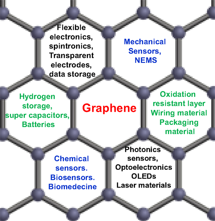
Figure 1. Various potential applications of graphene material.
Experimentally measured properties of graphene have not only exceeded those obtained in any other material but also reached very often its theoretically predicted limits. A typical example is its room-temperature carrier mobility, of 2.5 × 105 cm2/Vs, which is found to be very close to the theoretical limit of 2 × 105 cm2/Vs (Mayorov et al., 2011). Many other representative examples could be found in the relevant literature, just to cite a few: a Young’s modulus of 1 TPa very close to that predicted by theory (Liu et al., 2007; Lee et al., 2008; Morozov et al., 2008); a thermal conductivity of 3000 W mK−1 (Balandin, 2011); an optical absorption of 2.3% in the infrared (Nair et al., 2008); its property to be completely impermeable to gases (Bunch et al., 2008); its ability to carry one million time higher densities of electrical current than copper (Moser et al., 2007), and its potential to be chemically functionalized (Elias et al., 2009; Loh et al., 2010; Nair et al., 2010). It is worth noting that the majority of these properties have been experimentally measured for a high-quality graphene samples, deposited on specific substrates, such as hexagonal boron nitride (Dean et al., 2010; Mayorov et al., 2011). However, similar properties have not been observed so far on graphene material prepared using classical techniques, although these conventional processes are continuously improving (Neto et al., 2009; Sarma et al., 2011). We conclude then that the challenge related to find markets of graphene applications is mainly related to the real progress realized in its mass production with appropriate characteristics.
The number of publications related to the graphene material is continually growing has increased dramatically especially in last years (from about 4000 in 2010 to more than 14,000 in 2014) (Choi et al., 2010). Figure 2 shows how the number of refereed articles dealing with graphene material has steadily increased since 2004, based on data collected from the Engineering Village web-based information service.
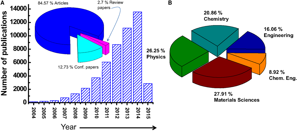
Figure 2. (A) Number of the publications/year on the graphene materials. The inset is the distribution of the document type, where only 2.7% of the publications are related to a review work. (B) Distribution of the publications by subject area.
The same tendency is also recorded with patents applications, which have downright doubled within 2 years only [i.e., from 2010 to 2012 with a total of 8416 patents worldwide by February 2013 (Zhang et al., 2013)].
In the recent years, there have been many review works, related either to theoretical and/or experimental studies, discussing the topics of synthesis and application of graphene material. To cite just few recent works, Neto et al., (2009) reviewed the electrical properties of graphene, and then focused on its electronic transport properties (Neto et al., 2009). Other experimental reviews included detailed discussions of synthesis (Zhang et al., 2010a) and Raman spectroscopy processes of transport mechanisms (Ni et al., 2008; Avouris, 2010; Giannazzo et al., 2011), related to electronic applications graphene, including transistors like-devices, bandgap engineering (Loh et al., 2010), and optoelectronic technologies (Bonaccorso et al., 2010; Schwierz, 2010). However, among all the published articles on the matter, only 18 review works have been conducted on the smart applications of the graphene materials (Figure 3), and to the best of our knowledge, only one review-article has been published on 2015. In sum, along with the increase in the number of publications in this area comes a need for a comprehensive review article, and the objective of this paper is to address this need. The literature is indeed lacking a comprehensive review of the recent experimental advancements on graphene material and its smart applications. This is the aim of our article. However, due to the huge number of various works that are involved, and often the unavailability of access to many conference proceedings, the emphasis of this paper was on the most accessible refereed journal articles. Obviously, it was not possible and practical to cover all of these articles, especially since a lot of them had already been covered by previous paper review; an attempt was made to select representative articles in each of the relevant categories. This review should be particularly well suited to graduate students who desire an introduction to the study of graphene that will provide them with many references for further reading.
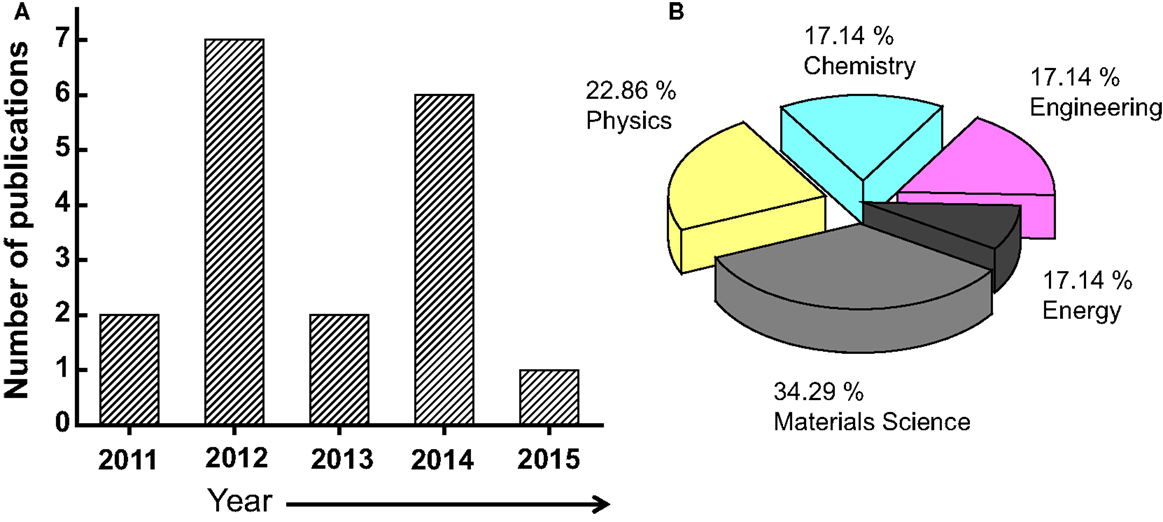
Figure 3. (A) Number of the review publications/year on the graphene materials. (B) Distribution of the review publications per subject area.
Graphene Scalable Synthesis Perspectives
Initially discovered by micromechanical exfoliation of graphite (Geim and Novoselov, 2007b), graphene has generated widespread interest as a smart material. However, for graphene to make a significant impact within industry, it is important to develop methods for scalable synthesis of high-quality graphene. The current common production methods for graphene include liquid exfoliation, ultrahigh vacuum processes, annealing of silicon carbide (SiC), and obviously, chemical vapor deposition (CVD). Other methods, which could be used for scalable graphene synthesis, include plasma enhanced CVD, flame synthesis, and pulsed laser deposition (PLD). These methods will be discussed in this review with a focus on identifying processes that can be translated for commercial production of graphene. This review does not cover methods for the production of graphene oxide.
Micromechanical Exfoliation
Micromechanical exfoliation involves peeling highly ordered pyrolytic graphite (HOPG) using adhesive tape (Novoselov et al., 2005). Since each layer of graphene is bonded to the other layer by van der Waals bonding, it is feasible to cleave HOPG. Normally, the peeling is performed several times. This process can also be used to produce few layers graphene (FLG). While this is the simplest method for the production of graphene and is commonly used in laboratory experiments, the production method is not scalable for large-scale graphene growth.
Liquid-Phase Exfoliation
Liquid-phase exfoliation (LPE) involves using a solvent to exfoliate graphite by ultrasonication (Hernandez et al., 2008; Lotya et al., 2009). Commonly used solvents include acetic acid, sulfuric acid, and hydrogen peroxide (Singh et al., 2011). The ultrasonication time is typically 60 min with a power of 250–500 W. Green and Hersam (2009) reported the use of sodium cholate as a surfactant for the exfoliation of graphene. Moreover, they were able to separate the sheets by density gradient ultracentrifugation, which enabled the isolation of graphene from FLG. LPE can be used for the production of graphene nanoribbons (GNRs) (Li et al., 2008), where the width is <10 nm. While LPE represents a scalable method for the production of graphene, large scale film growth remains really challenging.
Chemical Vapor Deposition Based Synthesis
Chemical vapor deposition of graphene involves the use of transition metals, where nickel (Ni) (Reina et al., 2008; Chae et al., 2009; Kim et al., 2009; Losurdo et al., 2011) and copper (Cu) (Li et al., 2009; Bae et al., 2010; Guermoune et al., 2011; Suk et al., 2011; Wang et al., 2011) are suitable for large scale production of graphene.
Graphene growth based on CVD has shown exceptional device properties (Figure 4) (Bae et al., 2010), with electron mobility of 7350 cm2 V−1s−1 (Novoselov et al., 2005). In addition, large scale production of 30″ graphene films was demonstrated using roll-to-roll CVD (Mattevi et al., 2011). The graphene obtained from this process was of high quality, with a sheet resistance of ~125 Ω/square and 97.4% optical transmittance.
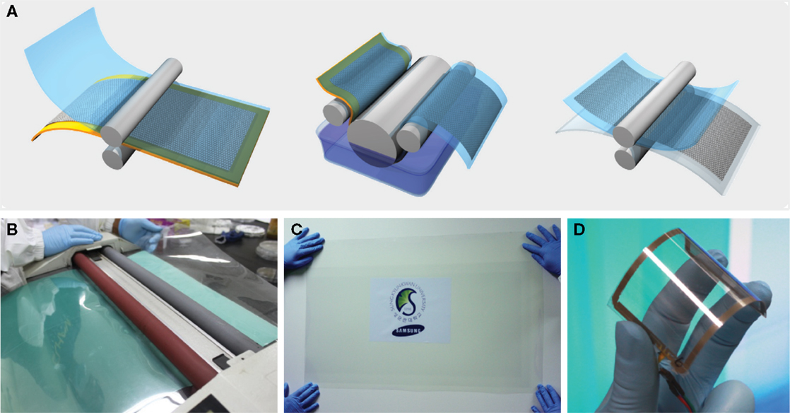
Figure 4. (A) Schematic of the roll-to-roll production of graphene films grown on a copper foil. (B) Roll-to-roll transfer of graphene films from a thermal release tape to a PET film at 120°C. (C) A transparent large-area graphene film transferred on a 35″ PET sheet. (D) An assembled graphene/PET touch panel showing mechanical flexibility. Reproduced with permission of Bae et al. (2010). Copyright 2010, Nature Nanotechnology.
Graphene growth using CVD is fairly straightforward, where a copper or nickel substrate is placed in a reactor at temperatures normally around 1000°C. The initial step in the process is to introduce hydrogen in the reactor. This step is critical to eliminate any oxide layer present in the metal, for the case of Cu this will reduce any native layers of CuO and Cu2O. The hydrogen atmosphere also enables the growth of grain boundaries (Mattevi et al., 2011), which is necessary for the growth of high-quality graphene. Afterwards, a hydrocarbon gas (typically methane) is added to the reactor. The hydrocarbon gas provides the necessary carbon species used in the growth of graphene. The hydrocarbon gas to hydrogen ratio plays an important role in the growth of graphene. If insufficient hydrogen is present, this could result in oxidized metal layers being present, which can lead to a disordered graphene structure. By contrast, excess hydrogen has shown to etch away graphene. On polycrystalline substrates, the graphene flakes tend to have different lattice orientations.
Using CVD, graphene is grown onto transition metals, which enables a low-energy pathway by forming intermediate compounds for the growth of graphene. The first row of transition metals Fe, Co, Ni, and Cu is of great interest due to their low cost and high availability. The difference in the carbon solubility between these metals impacts the growth quality, where Fe has the highest and Cu has the lowest carbon solubility. For this reason, Cu is an ideal metal for growing single layer graphene. When using Ni and Co it is common to get up to 10 layers of graphene. Similarly, on Fe it is common to have FLG.
Most practical applications of graphene require that the underlying surface be insulating. For this reason, graphene must be transferred to an insulating surface, such as SiO2 (Bhaviripudi et al., 2010). Additionally, this transfer is required to measure the optoelectronic properties of the synthesized graphene. The commonly used process to transfer graphene is to first deposit and cure poly (methylmethacrylate) (PMMA) on the metal sheet. Afterwards, etch the Cu metal sheet using iron chloride. This gives a floating sheet of PMMA and graphene, which is rinsed in deionized water. Subsequently, transfer this layer to an insulating surface and use acetone to remove the PMMA layer.
Plasma Enhanced Chemical Vapor Deposition Synthesis
Plasma enhanced CVD (PECVD) is another method used for the synthesis of graphene that is comparable to the thermal CVD process (Zhu et al., 2007; Yuan et al., 2009; Kim et al., 2011; Bo et al., 2013). PECVD is based on a number of plasma sources, such as microwave (MW) (Malesevic et al., 2008), radio frequency (RF) (Wang et al., 2004), and direct current (dc) arc discharge (Krivchenko et al., 2012) have been utilized in the growth of graphene. Copper and nickel are typically used as the substrate for PECVD graphene growth; however, a number of additional substrates have also been used (Dato et al., 2008; Bo et al., 2013). A particularly exciting technique is a substrate free method based on the decomposition of ethanol in MW-based PECVD reactor (Guermoune et al., 2011). Such methods provide can be used for scalable production of graphene powder. Typical growth conditions of PECVD graphene on a substrate are 5–100% CH4 in H2 with a substrate temperature of 500–800°C (Singh et al., 2011; Bo et al., 2013). The power of the plasma is 900 W. Such processes can enable the growth of graphene at lower temperatures and shorter duration (<5 min). However, the quality of the graphene film is typically lower when compared to thermal CVD.
The growth of graphene films at low temperature is important for a number of applications. For instance, fabrication of graphene for high-performance display glass has to be at a temperature lower than 660°C (Ren et al., 1998; Bo et al., 2013). Furthermore, production at lower temperature can provide new manufacturing opportunities in the area of flexible electronics based on plastics (Tung et al., 2009). Critical challenges still need to be overcome, as at lower temperatures the graphene film tends to have a higher disorder.
Flame Synthesis
Flame synthesis is extensively used to produce commercial quantities of nanoparticles. Of the most widely used nanoparticles, carbon black, fumed silica, and titania, flame synthesis is the dominant method in the production of these materials. Volumetric production of the flame synthesis industry is on the order of 100 metric tons per day (Kammler et al., 2001). A key advantage of flames is that it readily provides the high temperature necessary for gas-phase synthesis along with a carbonizing or oxidizing environment.
With respect to graphene, flame synthesis is not as commonly studied when compared to CVD, but it offers several important advantages, such as scalability and cost effectiveness. The most commonly used flame types include premixed, normal diffusion, inverse diffusion, and co-flow (Inoue et al., 2010; Memon et al., 2013). Since early 2000s, a number of researchers have focused on the use of flames for CNT synthesis (Inoue et al., 2010). However, the development of flame synthesis for graphene is still in its early stage. In addition to flame type, other parameters including temperature, species concentration, and velocity impact the growth process. Graphene being a two-dimensional material requires large-scale production across a substrate. Due to the temperature and species gradients that occur in most flames it is difficult to scale the growth of graphene across an entire substrate. Moreover, a reduced environment with carbon rich species, which is necessary for graphene growth, is difficult to achieve in most flames. Nevertheless, flame synthesis has the potential to economically enable the mass production of graphene.
Similar to earlier CNT flame synthesis papers, where the growth of CNTs was observed near the soot region of a premixed flame, carbon particles containing graphene were observed in Bunsen (propane) flame (Ossler et al., 2010). These particles were collected by placing a transmission electron microscopy grid 2 cm above the tip of the burner. The grid was held within the flame for 10–50 ms. The graphene films were several hundreds of nanometers in size.
In an attempt to grow graphene on copper, Li et al. (2011b) investigated the growth of graphene using an ethanol burner. The substrate was placed within the flame at a temperature of 550–700°C and the flame was extinguished using a cap to prevent the oxidation of the copper foil. The growth of an amorphous carbon film was observed on the substrate and XPS confirmed the formation of sp2, sp3, and C–O bonded atoms. Graphene was not observed due to the low temperature and the presence of oxygen within the flame. In a different experiment, Li et al. (2011a) were able to synthesis graphene successfully on nickel. The process utilized two different burners (burner 1 and burner 2), with the substrate situated within the interior region of the flame structure itself (Figure 5). Burner 1 (alcohol burner) surrounded the substrate for the entire time, where it prevented air oxidation and served as the carbon source. Burner 2 (butane-fueled Bunsen burner) provided the additional heating of the substrate and served as the carbon source for graphene growth. The flame was extinguished using a cap. There are still numerous challenges in using flame synthesis for the growth of graphene, specifically in developing methods that result in higher quality graphene.
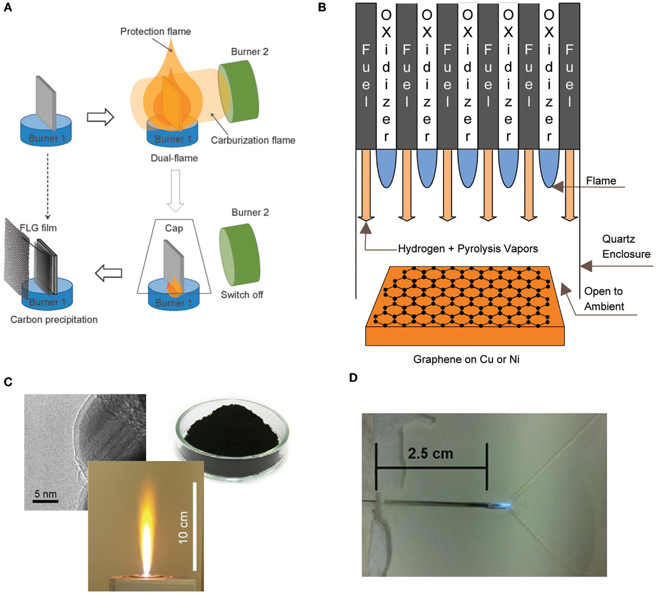
Figure 5. Different configurations used for the flame synthesis of graphene, (A) dual flame configuration, (B) multiple inverse diffusion flames, (C) flame spray pyrolysis and (D) microcombustor. Reproduced with permissions from Luechinger et al. (2008), Li et al. (2011b), Memon et al. (2011), and Kellie et al. (2013).
Epitaxial Growth on Silicon Carbide Substrate
Yannopoulos et al. (2012) have investigated the thermal decomposition of SiC surface, which was providing an epitaxial growth of graphene material (Figure 6). They reported a new process using a CO2 laser as the heating step for a fast and one-step growth process of large uniform graphene film on SiC. This method can control the stacking order of epitaxial graphene and is cost-effective since it does not involve any pretreatment step or high-vacuum process. The decomposition operated at low temperature and proceeded in the second time scale, thus providing a means to engineering graphene patterns on SiC by focused laser beams.
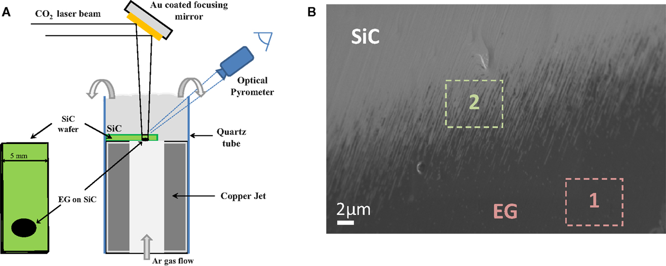
Figure 6. (A) Schematic diagram of the CO2 laser induced epitaxial growth of graphene on SiC wafers. (B) SEM micrograph showing the formation of epitaxial growth graphene (Zone 1) on 6H-SiC (0001). Reproduced with the permission from Yannopoulos et al. (2012). Copyright 2012, Wiley-VCH.
Pulsed Laser Deposition
The PLD process is definitely considered as one of the most versatile growth approaches. Since the laser energy source is located outside the deposition chamber; the use of either ultrahigh vacuum or ambient gas becomes possible (Krebs et al., 2003). Combined with a stoichiometry transfer between ablated target and substrate where the material is deposited, this flexibility allows depositing theoretically all possible kinds of materials, including polymers or fullerenes (Eason et al., 2006). This technique was first employed by Smith et al. (1965) (Krebs et al., 2003) in 1965 to elaborate semiconductors and dielectric thin films. In 1987, it was then fully developed by Dijkkamp et al. (1987) for the deposition of high-temperature superconductors. Their work allowed to define the main characteristics of PLD, namely, the stoichiometry transfer between target and deposited film (Smith et al., 1965; Dijkkamp et al., 1987; Chrisey and Hubler, 1994; Eason et al., 2006). Since the work of Dijkkamp et al., the deposition technique has been extensively used for all kinds of oxides, nitrides, carbides and also for preparing metallic systems and even polymers or fullerenes (Krebs et al., 2003). During PLD, almost all experimental parameters can be adjusted to control the film growth, and ranging from the laser parameters (Fluence, wavelength, pulse-duration, and repetition rate), to the deposition conditions (target-to-substrate distance, temperature, nature of the gas, pressure, etc.).
A representative schematic diagram for PLD (Krebs et al., 2003) is shown in Figure 7. Inside the vacuum chamber (ultrahigh vacuum, UHV), targets of elementary or alloy elements are struck at an angle of 45° by a high energy focused pulsed laser beam. The atoms and ions ablated from the target(s) are then deposited directly on the substrate (Krebs et al., 2003). In the majority of the cases, the substrates are attached with their surfaces parallel to the target(s) surfaces at a distance of 2–10 cm.
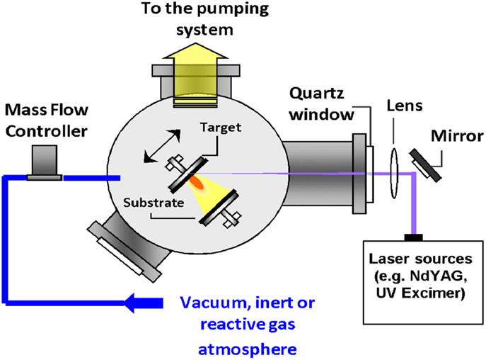
Figure 7. Schematic of a representative laser deposition tool.
To the benefit of the reader, Figure 8 summarizes the main first-deposited materials since the introduction of PLD in 1987, with respect to the year for deposition and corresponding reference.
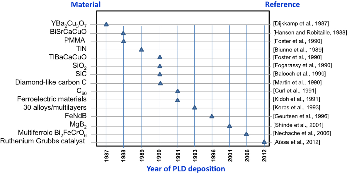
Figure 8. List of the materials deposited for the first time by PLD after 1987.
As mentioned earlier, in the PLD process, one of the main advantages is the fact that during deposition, the stoichiometry of the deposited material is very close to the target (Krebs et al., 2003). Consequently, it is possible to prepare stoichiometric thin films from a single alloy bulk target (Krebs et al., 2003).
In the context of the graphene growth, and in parallel to the CVD deposition method, physical vapor deposition has also been reported for the growth of graphene (Koh et al., 2010; Zhang and Feng, 2010b). In UHV, PLD chambers graphite is normally used as the target with a transition metal as the substrate (Figure 9). A substrate temperature of 1300°C was reported for 1–2 layers of high-quality graphene (Figure 9) (Zhang and Feng, 2010b). No carbide formation occurs at the interface of graphene and the metal (Zhang and Feng, 2010b). While numerous metals can be used as a catalyst, nickel appears to be the most promising for low temperature growth. Numerous parameters, such as the cooling rate and laser power, impact the quality of graphene films (Koh et al., 2010).
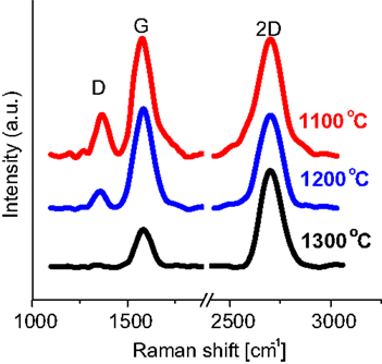
Figure 9. Graphene deposition by means of PLD. Measured Raman spectra with respect to the growth temperature. Reproduced with permission from Zhang and Feng (2010b). Copyright 2010, Elsevier.
Laser-Based Chemical Vapor Deposition
A continuous wave (CW) laser is utilized for laser-based CVD in an enclosed chamber (Figure 10A) (Park et al., 2011). The precursor gases used include methane and hydrogen, with Ni foil as the substrate. The synthesis mechanism is based on a vapor–liquid–solid that only takes nanoseconds to picoseconds. The spectra of the Raman spectroscopy showing the different graphene layers are illustrated in Figure 10B. A key advantage of this process is that it can be used for graphene lithography, where the laser can be scanned on specific areas of a metal catalyst enabling direct growth.
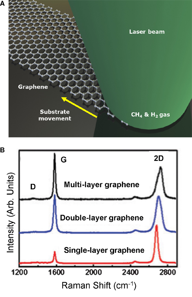
Figure 10. (A) Schematic of the laser induced CVD process, and (B) mea-sured Raman as a function of the number of graphene layers. Reprinted with permission from Park et al. (2011). Copyright 2011, American Institute of Physics.
Laser Growth Directly on Silicon and Quartz Substrates
Sun et al. (2010) produced graphene on Cu and Ni film using PMMA. Due to the existence of the metal films, the graphene films need be transferred to other substrate using polydimethylsiloxane (PDMS) or PMMA (Kim et al., 2009; Reina et al., 2009; Sun et al., 2010). Silicon wafer is the most important single-crystal substrate used for semiconductor devices and integrated circuits (ICs). Suemitsu et al. (2010) produced epitaxial graphene on Si substrate. In their approach, a SiC film of about 100 nm-thick was deposited on the Si wafer before growth, so graphene was grown on the SiC surface. Direct growth of graphene on bare Si substrate without any other material is very attractive. Graphene films can form a Schottky junction with Si, which can produce a built-in electric field and realize electron-hole separation, and has been used to fabricate solar cells (Li et al., 2010a; Gunst et al., 2011; Karamitaheri et al., 2011).
Wei and Xu (2012) have demonstrated the growth of FLG directly on a silicon substrate using a laser irradiation. Silicon substrates were coated with PMMA, which was then evaporated using a CW laser beam. The laser beam also melts the silicon surface and carbon atoms from PMMA separates from the silicon upon cooling to form FLG. A substrate of 1 cm × 2 cm p-type (111)-oriented Si wafer was used to grow graphene. The silicon wafer was first cleaned and the native oxide layer was removed in buffer hydrofluoric acid (HF) solution to form H-terminated silicon surface. A PMMA layer was coated on the Si surface by spin coating, then covered by a quartz wafer of the same size, and then fixed on a sample stage using two spring clamps. The purpose of using the quartz wafer is to maintain a high enough concentration of carbon after PMMA is evaporated and dissociated by laser irradiation. The growth was conducted in a vacuum chamber using a CW that was directed on the Si surface to melt the surface of the Si wafer.
For the synthesis of graphene on metal, two main growth mechanisms were proposed. On Ni, graphene was produced via carbon dissolution and precipitation (Yu et al., 2008). On Cu, the growth can be explained by surface-catalyzed process, which involves carbon nucleation on the Cu surface, and the growth of graphene with the addition of carbon to the edges (Wei and Xu 2012). However, both of these growth mechanisms cannot explain the graphene growth on Si. Cu or Ni maintains solid in the graphene growth process. They found that if the laser power was below the melting point of silicon, there was no graphene grown on the silicon surface.
Similar work has been achieved by Wei et al. (2013), who grow FLG (2–3 layers) on quartz substrate by using a continuous-wave laser by suing a photoresist S-1805 coated on the quartz wafer (thickness 30 nm).
Applications of Graphene Materials in Functional Devices
Graphene research has skyrocketed since the Nobel Prize winners Andre Geim and Konstantin Novoselov published a number of papers on the discovery of graphene 11 years ago. Since then, there has been a sharp increase in our scientific knowledge of graphene, as shown by the number of publications and patent applications on graphene (Figure 2). However, only a handful of graphene-based devices have entered the market, thus we are in an early stage in the commercialization of this material. Further research and development of graphene are critical to help achieve the full potential of this material and the sections below relate to research work of using graphene in smart applications. Figure 11 shows attempt of classification of some potential smart applications of graphene material as a function to the corresponding technology readiness level.
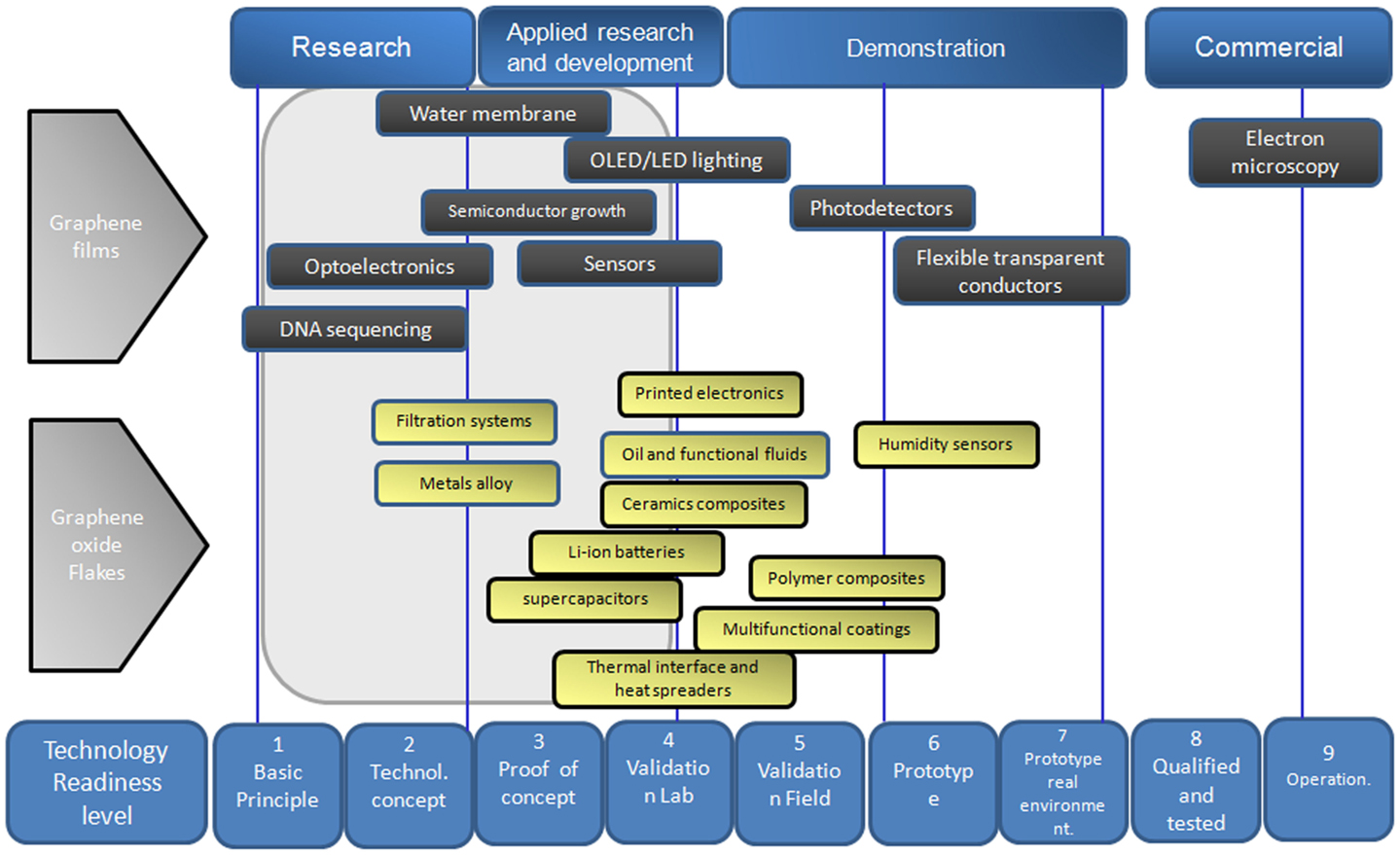
Figure 11. Potential smart applications of graphene material as a function to the technology readiness level.
Photovoltaic Cell
Photovoltaic (PV) cell is the device which converts light to electricity (Chapin et al., 1954; Wang et al., 2008). So far, graphene-based solar cells have been demonstrated in dye-sensitized PV cells (Choe et al., 2010; Jo et al., 2012), organic bulk-heterojunction PV cells (Li et al., 2010b; Yin et al., 2010), hybrid ZnO/poly(3-hexylthiophene) (P3HT) PV cells (Li et al., 2010c), Si based PV cells (Shim et al., 2011), and InGaN p-i-n PV cells (Gomez De Arco, 2010).
The functionalization of graphene material either during synthesis process (in situ) or post-treatment has demonstrated not only the possibility to control the properties of the surfaces and interfaces but also tailoring its work function (Jo et al., 2010; Guo et al., 2011; He et al., 2011; Wan et al., 2011). In an organic PV cell, the difference in work function between the two conductors creates an electrical field in the organic layer (Jo et al., 2012). To date, the power conversion efficiency (PCE) of graphene-electrode organic solar cells (OSCs) has been reported to be in the range of 0.08–2.60% (Wan et al., 2011; Jo et al., 2012), which is indeed much lower than those of conventional OSCs made with ITO electrodes (8.37%) (Stankovich et al., 2006; Chen et al., 2010a; He et al., 2011; Wan et al., 2011; Yu et al., 2012; Saravanakumar et al., 2013; Yokomizo et al., 2013; Sharma et al., 2014). However, the PCE of graphene-electrode OSCs needs to be improved to make graphene film a serious candidate for OSCs (Jo et al., 2012).
Transparent and Flexible Electronics
Currently, most of the research groups in electronics devices fabrication are investigating different routes to fabricate flexible and transparent electronic devices for various types of applications, including smart windows, IC cards, displays, LEDs, solar cells, etc. (Wager et al., 2003; Yu et al., 2011; Jo et al., 2012). In materials, graphene is one of the viable aspirants, which have all the required properties, at the same time, such as optical transparency, mechanical flexibility, and high conductivity. In recent years, different research groups have reported the integration of graphene-based composite electrodes, including graphene/pentacene and graphene/SWCNT, into transparent and flexible electronic like-devices, such as transistors, memory devices, and ICs (Wager et al., 2003; Ji et al., 2011; Lee et al., 2011; Yu et al., 2011; Jo et al., 2012).
Pentacene-based organic FETs-devices were elaborated onto a flexible substrate by means of patterning and transfer or transfer and patterning processes (P-T) and (T-P) techniques that are defining the graphene electrodes (Figure 12A) (Lee et al., 2011; Jo et al., 2012). As a gate electrodes, a plastic substrate based on PEDOT/PSS was used, and poly-4-vinylphenol (PVP) as cross-linker. The typical transfer response of these organic FET is shown in the Figure 12A, where a carrier mobility of 0.01 and 0.12 cm2/Vs were systematically estimated for the (T-P) and (P-T) processes, respectively (Jo et al., 2012). In addition to the field effect carrier mobility, the overall electronic characteristics of the organic transistors dealing with the (P-T) technique of graphene are superior (Jo et al., 2012). Figure 12B is showing the variation of the electrical resistance as a function of the number of graphene layers. However, there is large room for improving these electronic properties, especially the carrier mobility and to make it more feasible to use in large scale applications (Jo et al., 2012).
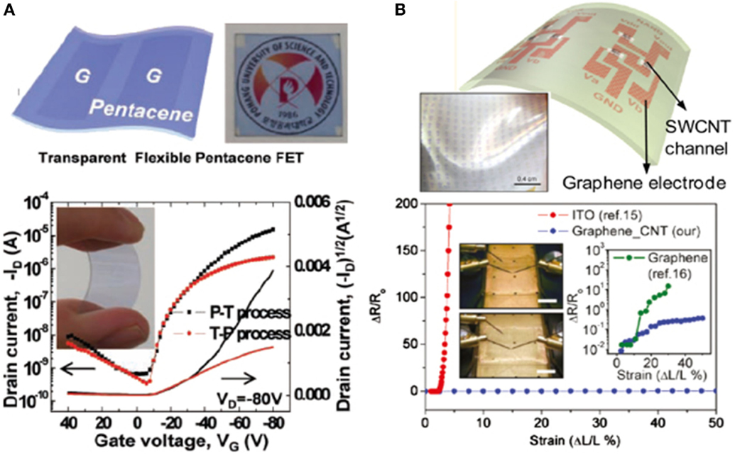
Figure 12. (A) Graphical representation and optical photo of an optically transparent and mechanically flexible FETs using graphene as source and drain electrodes. (B) Graphical representation composite graphene/SWCNT composite electrode network in FETs and its photograph. Inset in (A) shows an image of a mechanically stretched graphene/SWCNT composite based transistor, at the 0 and 50% strain, respectively; the right inset (B) is showing the variation of the electrical resistance w/r to the graphene number of layers. Reproduced with permission of Lee et al. (2011). Copyright 2013, Wiley-VCH.
Smart Applications of Graphene
Thermoelectric Application of Graphene
Thermoelectric materials (TEM) achieve the conversion between thermal and electrical energy and vice versa. This field has regained renewed attention because of the huge potential of TEM to be applied in Peltier coolers and thermoelectric power generators. It is well established that the performance of TEM are determined mainly by its dimensionless figure of merit, namely ZT. To date, the performance research of TEM have mainly focused on inorganic semiconductors, such as PbTe, Bi2Te3, CoSb3, SnSe, and theirs alloys or composites (Li et al., 2010d). The challenge to develop TEM for a crystalline system with high performance is know how to tailor the interconnected thermoelectric physical parameters, including Seebeck coefficient, the electrical conductivity, and thermal conductivity.
The efficiency of a TEM-based device is usually characterized by the following figure of merit:
where S is the Seebeck coefficient (or thermopower, μV/K), σ is the electronic conductance (S/m), T is the thermal conductivity including contributions from both phonons and electrons (W/mK), and κ is the absolute temperature (K).
Figure 13 shows a schematic illustration of a thermoelectric module for (a) power generation (Seebeck effect) and (b) active generation (Peltier effect). Figure 13A shows an applied temperature difference, which causes charge carriers in the material (electron or holes), to diffuse from the hot side to the cold one, resulting in a current flow through the circuit. Figure 13B is schematic of the heat that evolves at the upper junction and is adsorbed at the lower junction when a current is made to flow through the circuit.
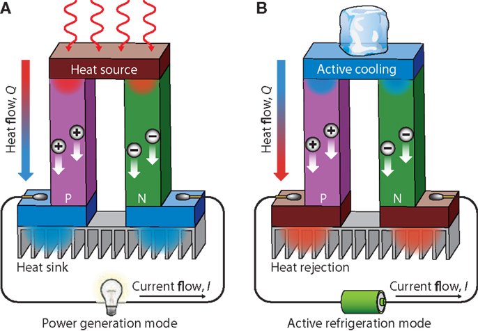
Figure 13. Schematic illustration of a thermoelectric module for (A) power generation (seebeck effect) and (B) active generation (Peltier effect). Reproduced with the Permission from Li et al. (2010d). Copyright 2010, NPG Asia Mater.
Recently, great effort has been made in improving the TEM dimensionless figure of merit (ZT). The difficulty in to simultaneously optimizing them, which causes thermoelectric research to stagnate for a while, until great reductions in thermal conductivity were theoretically and experimentally proven in nanostrtuctured materials.
Ghosh et al. (2010) examined the evolution of the thermal properties of FLG with respect to increasing thickness (i.e., the number of graphene layer, n). The results obtained by Raman spectroscopy have shown that, overall, the thermal conductivity decreases with increasing the FLG thickness, approaching that of the bulk graphite limit (Figure 14) (Ghosh et al., 2010). The experimental data points in Figure 14 were all normalized to the same width of graphene sheet of 5 μm (Ghosh et al., 2010). The detailed procedure is described in Ghosh et al. (2010).
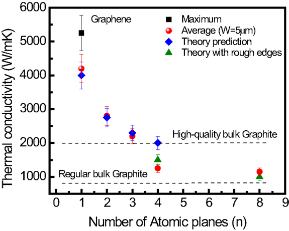
Figure 14. Thermal conductivity with respect to the number for atomic planes of quasi-2D carbon materials. Experimental and simulated thermal conductivity of suspended FLG as a function of number of atomic layer, n, taken at the fixed width, W of the graphene flake. Reproduced with the permission from Ghosh et al. (2010). Copyright 2011, Nature Materials.
The evolution observed from 2D graphene to bulk graphite is explained by the cross-plane coupling of the low-energy phonons and changes in the phonon scattering, since more states are available for scattering owing to the increased number of phonon branches. The thermoelectric power (TEP) is the voltage developed across a sample when a constant temperature gradient is applied. TEP of 80 μV/K was recently measured in graphene at room temperature (300 K) (Zuev et al., 2009). Similar to the quantum Hall effect in electronic transport, quantized TEP has also been observed in graphene at high-magnetic fields (Zuev et al., 2009). The TEP can be tuned in graphene, even to negative values, under the application of a gate bias or chemical potential (Wei et al., 2009). Very large TEP values have been predicted for GNRs, for instance, 4 mV/K for a 1.6 nm wide ribbon (Haskins et al., 2009). In comparison, the highest value experimentally reported so far is 850 μV/K for two-dimensional electron gases in SrTi2O3 heterostructures (Ohta et al., 2007), while only a few μV/K has been reported for bulk graphite (Tyler et al., 1953). The TEP power of single walled carbon nanotubes (SWNTs) has been theoretically and experimentally shown to be 60 μV/K (Hone et al., 1998), inferior to that of graphene. A giant thermoelectric coefficient of 30 mV/K was reported in metallic electrodes periodically patterned over graphene, deposited on SiO2 substrate (Chang et al., 2007).
On the other hand, thermoelectric properties of graphene have attracted increased interest as well, since it can convert heat to electricity and vice versa. A high thermopower value of 80 μV/K was reported for graphene (Zhu et al., 2009; Zuev et al., 2009). Various structures of graphene have been examined, including nanoribbons (GNRs) (Haskins et al., 2009; Sevinçli et al., 2009; Ouyang and Hu, 2010; Huang et al., 2011; Mazzamuto et al., 2011), quantum dots (Yan et al., 2012), graphene junctions, and chevron-type structures (Chen et al., 2010b). It is worth noted here that ZT of zigzag GNRs can exceed 3 (Ouyang and Hu, 2010).
Recently, many works have been conducted on the creation of graphene band gap by means of making an array of holes (antidots) into the graphene layer (Pedersen et al., 2008; Ouyang et al., 2011; Petersen et al., 2011; Chang and Nikolic, 2012). This is an inevitable property for the integration of graphene material directly into transistor architecture (Ouyang et al., 2011; Petersen et al., 2011). The gap can be engineered by controlling the lattice geometry (i.e., the antidot size and the hole-to-hole separation) (Shen et al., 2008; Eroms and Weiss, 2009; Bai et al., 2010; Kim et al., 2010; Gunst et al., 2011; Karamitaheri et al., 2011). Further, thermoelectric properties of these structures (2D graphene antidot lattices) have also been investigated where ZT up to 0.3 was found (Li et al., 2010d).
Graphene in Shape Memory Materials
Shape memory polymers (SMPs) are defined as smart materials, with the faculty to respond to an external stimulus, typically heat, and have a wide-range of applications from biomedical devices to space materials (Han and Chun., 2014). Polyurethane (PU) is the most attractive SMP material, commonly referred to as SMP polyurethane (SMPU) (Lee et al., 2014). Based on the specific molecular design, SMPU can form either a crystalline or amorphous structure, with a broad actuation temperature range from −20 to 150°C (Kim et al., 2014). SMP composites based on nanofillers have shown to increase the overall shape memory properties. An exciting research area is the use of carbon-based nanomaterials, particularly graphene, as nanofillers for SMPUs.
Han and Chun (2014) prepared a graphene/PU composite material by functionalizing graphene with diazonium salts carrying phenethyl alcohol. The resulting material showed enhanced shape memory, thermal, and mechanical properties. The resulting material showed shape fixity up to 98 with 94% shape recovery ratio after four cycles. Hysteresis loss can be low as 2%. Rana et al. (2013) prepared a flexible and conductive shape memory composite based on PU and functionalized graphene sheets. The graphene sheets were functionalized using phenyl isocyanate and poly diol. The composite resulted in 97% shape recovery and 95% shape fixity (see Figure 15). Modifications to PU can also improve the shape memory performance with graphene. Thakur et al. (2013) have demonstrated that castor oil-modified hyperbranched PU and graphene-oxide (without functionalization) can result in a shape recovery of ~99.5% with shape fixity of ~90%. Park et al. (2014) have demonstrated that PU and allyl isocyanate modified graphene oxide can also be actuated by infrared absorption, with a resulting shape recovery of 90%.
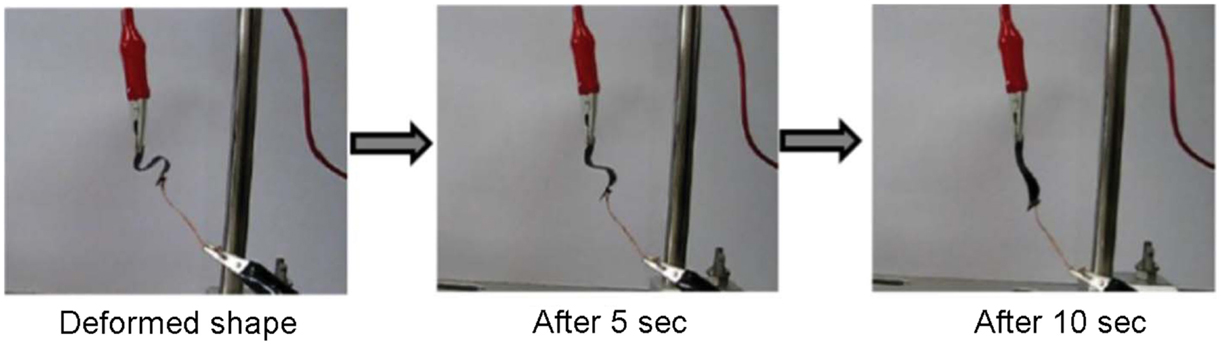
Figure 15. Shape recovery behavior of graphene-cross linked PU composites, for a temporary helix shape (left) to a permanent shape when applying a constant voltage of 50 V. Reproduced with permission from Rana et al. (2013). Copyright 2013, Royal Society of Chemistry.
Graphene in Self-Healing Materials
Long-term stability and durability of materials are one of the main challenges faced today for structural and coating applications, especially when using polymeric composites materials. Indeed, there are many parameters affecting the degradation of materials, including environmental conditions of large types (temperature gradient, UV irradiation, oxygen erosion, corrosion, etc.). As indicated by their name, self-healing materials are first conceived and then designed and elaborated to have the potential to heal mainly the mechanical properties of the materials when damaged. Representative applications of self-healing materials are found in composite polymers, various metals, ceramics, and their related composites, which are subjected to a wide variety of healing principles.
Recently, a few studies have demonstrated the potential of graphene as an additive for self-healing materials. Dong et al. (2013) synthesized a composite material of poly(acrylamide) (PAM), poly(acrylic acid) (PAA), and graphene that exhibits shape memory effect and self-healing ability. Graphene content was in the range of 10–30% and the material can be recovered after 20 cycles of cut and self-healing. The self-healing capabilities are illustrated in Figure 16, where 10 wt.% graphene sample is cut in the middle and the two pieces were healed together at 37°C for 20 min. The results suggest that the self-healing ability and shape memory effect occur due to a “zipper effect” of PAM–PAA that forms or dissociate the hydrogen-bond network, where such effects are limited without the addition of graphene. Huang et al. (2013) have demonstrated the use of FLG with thermoplastic polyurethane (TPU) as self-healing material initiated using an electric stimulus. When the FLG loading rate is 5 wt.%, the material can be healed to an efficiency higher than 98% in 3 min. Furthermore, upon increasing the FLG loading rate to 8 wt.%, the same healing efficiency of 98% can be achieved in 15 s only. It is expected that graphene efficiently converts electrical energy to thermal energy, which improves the self-healing ability of TPU diffusion and re-entanglement of the TPU chains. More recently, Wang et al. (2013) and Sullivan et al. (1977) have recently reported the fabrication of a composite based on a cross-linked (CL) hydrogen bonding polymer with graphene oxide. This composite material was found to enable a fast self-healing capability, with high efficiency, occurring at room-temperature. More importantly, the healing reaction was produced without the need of any external stimuli, such as electrical bias, light, and heat (Zhang et al., 2014). The introduction of the graphene material in this CL-based polymer was found to be crucial to reduce the needed amount of CL sites that are necessary for the healing reaction. It is worth noting here that a huge amount of CL sites are not only negatively impacting the mechanical properties of the polymer (including flexibility) but also its dynamic characteristics (Zhang et al., 2014). Such nanocomposite materials involving CL-hydrogen bonding polymer with graphene-oxide can be useful in many applications, e.g., protecting barrier for electronic devices, sealing layer for gas systems, and stretchable self-healing conductive wires (Zhang et al., 2014).
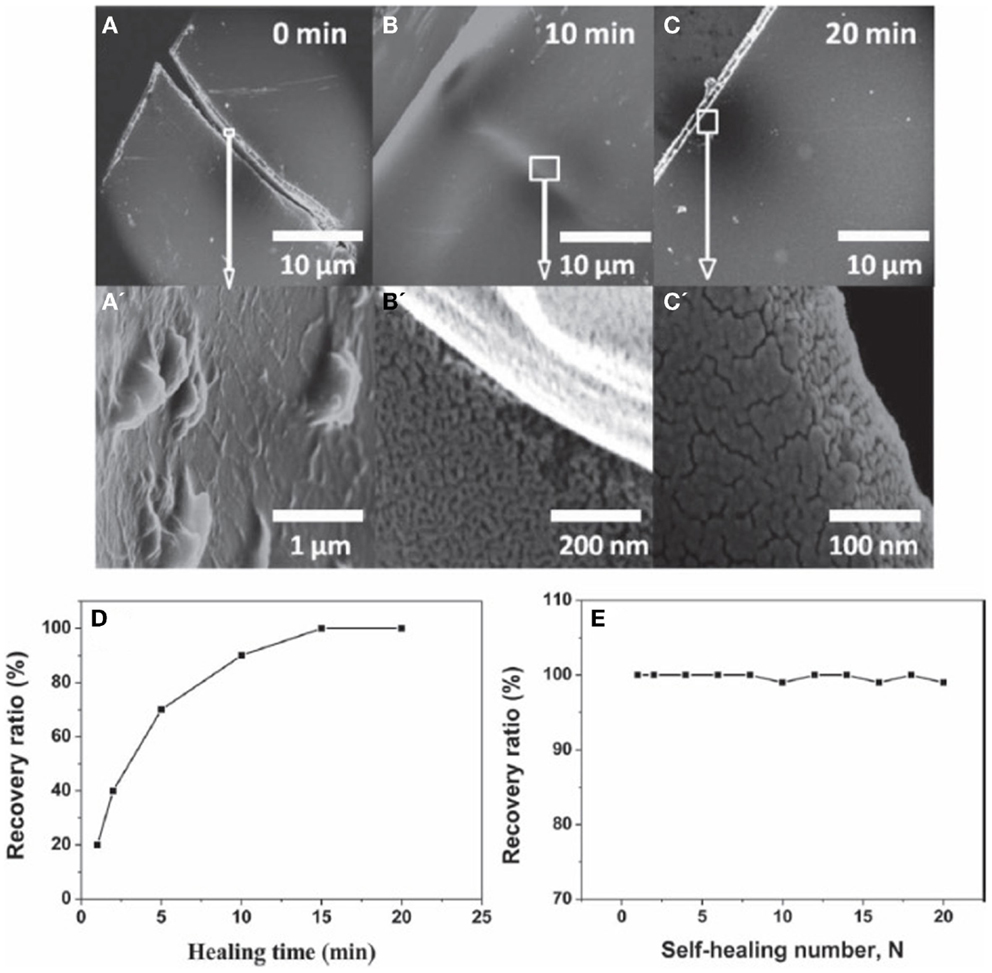
Figure 16. SEM image of G-PAM-PAA strip heating at 37°C in different times, (A) 0 min, (B) 10 min, and (C) 20 min. (A′–C′) are close-up view of the factures occurred in (A–C), respectively. Percentage of the recovery ratio as a function of (D) healing-time and (E) self-healing number (N). Reproduced with permission from Dong et al. (2013). Copyright 2013, Wiley-VCH.
Graphene in Photomechanical Actuators
Actuators are materials, which change their shape or dimensions under the application of external stimulus. To date, the well-recognized materials for actuation are piezoelectrics (Nakamura et al., 1989), ferro-electrics (Kuribayashi et al., 1989), shape memory alloys (Damjanovic and Newnham, 1992), electrostrictive materials (Damjanovic and Newnham, 1992), and conducting polymers (Smela et al., 1999). Recently, large stresses and strains from low-voltage electromehcanical actuation have exhibited by carbon nanotubes (CNTs) (Baughman et al., 1999) and porous metallic nanoparticles (Ahir and Terentjev, 2005). Beside this, both single walled CNT (SWCNT) and multiwalled CNT (MWCNT)-based composites have been reported to undergo photomechanical actuation (Dreyer et al., 2010).
Several articles have reported about graphene-based composites, mostly in sheets form and have derived from graphite oxide or graphite intercalation compounds (GICs). It has been observed that intrusion of graphite oxide or graphite intercalation compounds derived fillers can enhance electrical conductivities of polymeric matrices (Gómez-Navarro et al., 2008), the Young’s moduli (Potts et al., 2011), and could easily be functionalized to tailor to host polymer properties (Sun et al., 2009). Now, it is well-known that by tailoring the number of layers of graphene nanoplateletes (GNP) and GNR, the overall properties of composite material change [such as saturable absorption (Casiraghi et al., 2007) and electric field assisted band gaps (Zhang et al., 2009)].
Loomis et al. (2012) have reported that a simple polymer composite system with photomechanical responses is realized solely by incorporation of a homogeneous dispersion of GNPs within a PDMS elastomer matrix. It has been observed that the actuation responses of GNPs/PDMS composites depend on the initial applied pre-strain as in CNT/PDMS composites. Photomechanical stress change 2.4–3.6 times is greater for GNP/PDMS composites, compared to any other tested form of nanocarbon. These stress changes reported are usable and recoverable work achieved by the actuators. Energy conversion factor (ηM) of 7–9 MPa W−1 for optical-to-mechanical is obtained during testing. Until now, this is a largest energy conversion factor of an extraordinary photomechanical effect exhibited by any material so far.
Graphene in Piezoelectric Materials
Piezoelectric material has the property of converting mechanical movement into electrical movement and vice versa. Traditionally, piezoelectricity is considered to be an intrinsic property of a particular material phase. Piezoelectric materials have been frequently used in a wide variety of applications from pressure sensors (Pereira and Castro Neto, 2009), to acoustic transducers (Guinea et al., 2010), to high voltage generators (Bunch et al., 2007) for dynamical control of material deformation by application of external electric force.
Luk’yanchuk et al. (2015) have found that piezoelectricity can be concocted into intrinsically non-piezoelectric materials such as graphene. This is a nanoscale new phenomenon and lacking a direct bulk analog (Luk’yanchuk et al., 2015). This new phenomenon has provided room for practical approach toward manipulation and dynamic control different concerns in nanodevices, such as optical, chemical, and electronic. Luk’yanchuk et al. (2015) have reported an extraordinary two dimensional piezoelectric effect, both on a strained and unstrained graphene junction. Interestingly, it has been formally attested that this 2D piezo effect is a direct consequence of the difference in the two work functions (of the two type of graphene) and hence to the charge transfer occurring from the biaxial strain when putting the two graphene types together (i.e., bend band structure). The effect has termed as the band-piezoelectric effect, which exhibits a massive magnitude due to the ultrathin structure of graphene (Luk’yanchuk et al., 2015).
Using this new type of piezo effect, a piezoelectric nanogenerator and a piezoresistive pressure sensor within a graphene nano-electro-mechanical-system (NEMS) platform have been demonstrated. In this novel device, the deformation caused by an AFM tip resulted in charge separation, due to the modified band structure of the bent membrane (Luk’yanchuk et al., 2015). Consequently, by using appropriate metal electrodes with suited work function, we can even collect the cumulated charge and produce an electrical voltage (Luk’yanchuk et al., 2015).
Graphene in Electrorheology Materials
Electrorheology (ER) material is a type of smart material where the rheological properties of the material can be reversibly transformed with the application of an external electric field (Zhang et al., 2010c, 2012; Yin et al., 2012; Zhang and Choi, 2014). An ER material is composed of polarizable particles suspended in an insulating medium and after applying an electric field the particles are polarized and form a column like structure. This modifies the rheological properties of the material, such as viscosity, shear stress, and dynamic modulus. Applications of such materials include damper systems, ER polishing, tactile displays, medical devices, and robotic actuators. Recently, graphene, r-GO, and GO, due to their unique properties, have gathered the interest of the scientific community as an additive for ER materials (Zhang and Choi, 2014). Zhang et al. (2010c) prepared colloidal r-GO using a modified Hummers method, which was used to prepare a nanocomposite material comprising of GO and polyaniline (PANI). The resulting material showed adjustable electrical conductivity, which has potential for use as an ER material. Additionally, Zhang et al. (2012) also prepared GO particles suspended in silicone oil, where the ER fluid is polarized and exhibits viscoelastic properties at various strains under an electric field.
Yin et al. (2012) prepared a novel ER suspension comprising of two dimensional PANI decorated GO sheets. With the application of an electric field, the suspension containing PANI and GO, shows higher ER effect when compared to pure PANI. The performance of the material is dependent on the thickness of the PANI coating applied to the GO sheets. Furthermore, Yin et al. (2013) prepared mesoporous silica-coated r-GO nanosheets as a dispersal for ER fluids. Silica coating limits the conductivity of graphene, which enables high polarization and ER response, with the application of an electric field particularly high-frequency AC electric fields. The silica shells also limit the restacking of graphene. Li et al. (2015) studied the ER effects of non-conducting GO and conducting r-GO comprise an insulating SiO2 shell. The results show that the GO/SiO2 has a higher ER response to DC and low-frequency AC electric fields, while the r-GO/SiO2 has a higher ER response to high-frequency AC electric fields. The different behavior can be explained by the impact of the polarization rate with regards to the inter-particle interaction.
Multifunctional Graphene Nanocomposite Foams for Space Applications
Space is the new frontier and new materials, devices, and technologies for aerospace applications represent now an emerging sector with significant employment prospects and opportunities for profit. Materials and devices used in space applications (e.g., satellites) should combine functionality with low weight and reduced volume, to optimize cost effectiveness. The main cost of a satellite is its launch into orbit (estimated at about 7 M$), therefore reducing weight and volume can significantly decrease the overall cost. Weight savings can be achieved by replacing heavy copper wiring, which accounts for example up to 4000 lbs of weight on a Boeing 747 and about one-third of the weight of large satellites (Meador et al., 2010), with low density carbon-based wiring cables. In addition, Joule heating from metallic parts requires additional components for cooling (radiators), thus adding to the overall weight and cost. The combination of superior electronic and thermal properties of graphene materials could potentially revolutionize the design and fabrication of light weight electrical and electronic devices to be used in space applications. In this context, graphene is a promising candidate because its ballistic electron transport limits Joule heating and should allow reductions in weight, volume, and subsequently total cost.
Another potential space application of graphene is its use as nanofiller to fabricate light weight and robust nanocomposite, to be used, e.g., as thermal barrier. Recently, graphene nanoplatelets having FLG with 1–5 layers and typical diameters ranging from 1 to over 100 μm have been successfully grown by a team from Michigan State University1. These nanoplatelets show, overall, similar properties to a single graphene layer while being mechanically much robust. In addition, their cost production can be lowered to be competitive to other carbonaceous additives and fillers. These nanoplatelets could be used as a nanoadditive into various polymer foams, increasing thereby their thermal, mechanical, and electrical properties, while the foam still maintains its unique structure and low density. This combination of unique properties has direct potential application as flame resistant in space technology.
Conclusion and Outlooks
Research on graphene has considerably enriched our understandings and applications of two-dimensional atomic crystal. The combination of unprecedented physical and chemical properties, including its extremely high strength, thermal and electrical conductivity, and mechanical flexibility, have harried scientists to investigate in-depth its real potential in delivering improvements to different devices in many technological and scientific fields, ranging from materials science to physics, chemical engineering, and even biology. In this review, we have presented an overview of the main gas-phase synthesis of graphene and its applications as smart material systems. The possibility of successfully integrating graphene directly into device, could not only improve the electrical and/or mechanical properties but also enable the realization of a wide range of applications, such as actuation, thermoelectricity, shape memory, and self-healing. However, this success is conditioned by the prior success to address the following issues: (i) developing a cost-effective growth process to synthesize functional graphene in a reasonable scale with acceptable degree of reproducibility, for the realization of practical applications; (ii) considering the unique electrical, mechanical, and optical properties of graphene, incorporation of these characteristics into the existing smart systems from an interdisciplinary point of view should be highly valued; (iii) finally, from practical view-point, its highly desirable to fabricate graphene multifunctional systems, that are responsive to multiple stimuli. Considering the current and ongoing achievements, it is believed that the smart applications of graphene systems with more functionality are expected to emerge as new complements – and/or even replacements – to existing conventional systems, especially in fields of electronics, energy, and space.
Conflict of Interest Statement
The authors declare that the research was conducted in the absence of any commercial or financial relationships that could be construed as a potential conflict of interest.
Acknowledgments
Authors thank the financial support of the Qatar Environment and Energy Research Institute and Qatar Foundation.
Footnote
- ^Space Technology missions directorate. The document is available at: http://www.nasa.gov/directorates/spacetech/strg/2012_nstrf_rollins.html
References
Ahir, S. V., and Terentjev, E. M. (2005). Photomechanical actuation in polymer-nanotube composites. Nat. Mater. 4, 491–495. doi: 10.1038/nmat1391
Aïssa, B., Nechache, R., Haddad, E., Jamroz, W., Merle, P. G., and Rosei, F. (2012). Ruthenium Grubbs’ catalyst nanostructures grown by UV-excimer-laser ablation for self-healing applications. Appl. Surf. Sci. 258, 9800–9804. doi:10.1510/icvts.2010.255588
Avouris, P. (2010). Graphene: electronic and photonic properties and devices. Nano Lett. 10, 4285–4294. doi:10.1021/nl102824h
Bae, S., Kim, H., Lee, Y., Xu, X., Park, J. S., Zheng, Y., et al. (2010). Roll-to-roll production of 30-inch graphene films for transparent electrodes. Nat. Nanotechnol. 5, 574–578. doi:10.1038/nnano.2010.132
Bai, J., Zhong, X., Jiang, S., Huang, Y., and Duan, X. (2010). Graphene nanomesh. Nat. Nanotechnol. 5, 190–194. doi:10.1038/nnano.2010.8
Balandin, A. A. (2011). Thermal properties of graphene and nanostructured carbon materials. Nat. Mater. 10, 569–581. doi:10.1038/nmat3064
Balooch, M. T., Tench, R. J., Siekhaus, W. J., Allen, M. J., Connor, A. L., and Olander, D. R. (1990). Deposition of SiC films by pulsed excimer laser ablation. Appl. Phys. Lett. 57, 1540–1542. doi:10.1063/1.103346
Basu, S., and Bhattacharyya, P. (2012). Recent developments on graphene and graphene oxide based solid state gas sensors. Sens. Actuators B Chem. 173, 1–21. doi:10.1016/j.snb.2012.07.092
Baughman, R. H., Cui, C., Zakhidov, A. A., Iqbal, Z., Barisci, J. N., Spinks, G. M., et al. (1999). Carbon nanotube actuators. Science 284, 1340. doi:10.1126/science.284.5418.1340
Bekaroglu, E., Topsakal, M., Cahangirov, S., and Ciraci, S. (2010). First-principles study of defects and adatoms in silicon carbide honeycomb structures. Phys. Rev. B 81, 075433. doi:10.1103/PhysRevB.81.075433
Bhaviripudi, S., Jia, X., Dresselhaus, M. S., and Kong, J. (2010). Role of kinetic factors in chemical vapor deposition synthesis of uniform large area graphene using copper catalyst. Nano Lett. 10, 4128–4133. doi:10.1021/nl102355e
Biunno, N., Narayan, J., Hofmeister, S. K., Srivatsa, A. R., and Singh, R. K. (1989). Low-temperature processing of titanium nitride films by laser physical vapor deposition. Appl. Phys. Lett. 54, 1519. doi:10.1063/1.101338
Bo, Z., Yang, Y., Chen, J., Yu, K., Yan, J., and Cen, K. (2013). Plasma-enhanced chemical vapor deposition synthesis of vertically oriented graphene nanosheets. Nanoscale 5, 5180–5204. doi:10.1039/c3nr33449j
Bonaccorso, F., Sun, Z., Hasan, T., and Ferrari, A. C. (2010). Graphene photonics and optoelectronics. Nat. Photon 4, 611–622. doi:10.1038/nphoton.2010.186
Boukhvalov, D. W., Katsnelson, M. I., and Lichtenstein, A. I. (2008). Hydrogen on graphene: electronic structure, total energy, structural distortions and magnetism from first-principles calculations. Phys. Rev. B 77, 035427. doi:10.1103/PhysRevB.77.035427
Bunch, J. S., van der Zande, A. M., Verbridge, S. S., Frank, I. W., Tanenbaum, D. M., Parpia, J. M., et al. (2007). Electromechanical resonators from graphene sheets. Science 315, 490–493. doi:10.1126/science.1136836
Bunch, J. S., Verbridge, S. S., Alden, J. S., van der Zande, A. M., Parpia, J. M., Craighead, H. G., et al. (2008). Impermeable atomic membranes from graphene sheets. Nano Lett. 8, 2458–2462. doi:10.1021/nl801457b
Casiraghi, C., Hartschuh, A., Lidorikis, E., Qian, H., Harutyunyan, H., Gokus, T., et al. (2007). Rayleigh imaging of graphene and graphene layers. Nano Lett. 7, 2711–2717. doi:10.1021/nl071168m
Casolo, S., Martinazzo, R., and Tantardini, G. F. (2011). Band engineering in graphene with superlattices of substitutional defects. J. Phys. Chem. C 115, 3250–3256. doi:10.1021/jp109741s
Chae, S. J., GüneŞ, F., Kim, K. K., Kim, E. S., Han, G. H., Kim, S. M., et al. (2009). Synthesis of large-area graphene layers on poly-nickel substrate by chemical vapor deposition: wrinkle formation. Adv. Mater. Weinheim 21, 2328–2333. doi:10.1002/adma.200803016
Chang, P.H. and Nikolic, B.K. (2007). Giant thermoelectric effect in graphene. Appl. Phys. Lett. 91, 203116. doi:10.1021/nl500755m
Chang, P. H., and Nikolic, B. K. (2012). Edge currents and nanopore arrays in zigzag and chiral graphene nanoribbons as a route toward high-ZT thermoelectrics. Phys. Rev. B 86, 041406. doi:10.1103/PhysRevB.86.041406
Chapin, D. M., Fuller, C. S., and Pearson, G. L. (1954). A new silicon p-n junction photocell for converting solar radiation into electrical power. J. Appl. Phys. 25, 676–677. doi:10.1063/1.1721711
Chen, Z., Berciaud, S., Nuckolls, C., Heinz, T. F., and Brus, L. E. (2010a). Energy transfer from individual semiconductor nanocrystals to graphene. ACS Nano 4, 2964–2968. doi:10.1021/nn1005107
Chen, Y., Jayasekera, T., Calzolari, A., Kim, K. W., and Nardelli, M. B. (2010b). Thermoelectric properties of graphene nanoribbons, junctions and superlattices. J. Phys. Condens. Matter. 22, 372202. doi:10.1088/0953-8984/22/37/372202
Choe, M., Lee, B. H., Jo, G., Park, J., Park, W., Lee, S., et al. (2010). Efficient bulk-heterojunction photovoltaic cells with transparent multi-layer graphene electrodes. Org. Electron. 11, 1864–1869. doi:10.1016/j.orgel.2010.08.018
Choi, W., Lahiria, I., and Seelaboyinaa, R. (2010). Synthesis of graphene and its applications: a review. Crit. Rev. Solid State Mater. Sci. 35, 52–71. doi:10.1080/10408430903505036
Chrisey, D. B., and Hubler, G. K. (1994). Pulsed Laser Deposition of Thin Films. New York, NY: John Wiley.
Dato, A., Radmilovic, V., Lee, Z., Phillips, J., and Frenklach, M. (2008). Substrate-free gas-phase synthesis of graphene sheets. Nano Lett. 8, 2012–2016. doi:10.1021/nl8011566
Damjanovic, D. and Newnham, R. E. (1992). Electrostrictive and piezoelectric materials for actuator applications. J. Int. Mat. Sys. Struct. 3, 190–208. doi:10.1177/1045389X9200300201
Dean, C. R., Young, A. F., Meric, I., Lee, C., Wang, L., Sorgenfrei, S., et al. (2010). Boron nitride substrates for high-quality graphene electronics. Nat. Nanotechnol. 5, 722–726. doi:10.1038/nnano.2010.172
Dijkkamp, D., Venkatesan, T., Wu, X. D., Shaheen, S. A., Jisrawi, N., Min-Lee, Y. H., et al. (1987). Preparation of Y-Ba-Cu oxide superconductor thin films using pulsed laser evaporation from high Tc bulk materials. Appl. Phys. Lett. 51, 619. doi:10.1063/1.98366
Dong, J., Ding, J., Weng, J., and Dai, L. (2013). Graphene enhances the shape memory of poly (acrylamide-co-acrylic acid) grafted on graphene. Macromol. Rapid Commun. 34, 659–664. doi:10.1002/marc.201200814
Dreyer, D. R., Park, S., Bielawski, C. W., and Ruoff, R. S. (2010). The chemistry of graphene oxide. Chem. Soc. Rev. 39, 228–240. doi:10.1039/b917103g
Eason, R. (2006). Pulsed Laser Deposition of Thin Films: Applications-Led Growth of Functional materials. Hoboken, NJ: John Wiley & Sons, Inc.
Elias, D. C., Nair, R. R., Mohiuddin, T. M., Morozov, S. V., Blake, P., Halsall, M. P., et al. (2009). Control of graphene’s properties by reversible hydrogenation: evidence for graphane. Science 323, 610–613. doi:10.1126/science.1167130
Eroms, J., and Weiss, D. (2009). Weak localization and transport gap in graphene antidot lattices. New J. Phys. 11, 095021. doi:10.1088/1367-2630/11/9/095021
Fogarassy, E., Fuchs, C., Slaoui, A., and Stoquert, J. P. (1990). SiO2 thin-film deposition by excimer laser ablation from SiO target in oxygen atmosphere. Appl. Phys. Lett. 57, 664–666. doi:10.1063/1.104253
Foster, C. M., Voss, K. F., Hagler, T. W., Mihailovi, D., Heeger, A. J., Eddy, M. M., et al. (1990). Infrared reflection of epitaxial Tl2Ba2CaCu2O8 thin films in the normal and superconducting states. Solid State Commun. 76, 651. doi:10.1016/0038-1098(90)90108-N
Geim, A. K. (2009). Graphene: status and prospects. Science 324, 1530–1534. doi:10.1126/science.1158877
Geim, A. K., and Novoselov, K. S. (2007a). The rise of graphene. Nat. Mater. 6, 183–191. doi:10.1038/nmat1849
Geim, A. K., and Novoselov, K. S. (2007b). The rise of graphene. Nat. Mater. 6, 183–191. doi:10.1038/nmat1849
Geurtsen, A. J. M., Kools, J.C.S., Wit, L., and Lodde, J.C. (1996). Pulsed laser deposition of permanent magnetic Nd2Fe14B thin films. Appl. Surf. Sci. 9698, 887–890. doi:10.1016/0169-4332(95)00541-2
Ghosh, S., Bao, W., Nika, D. L., Subrina, S., Pokatilov, E. P., Lau, C. N., et al. (2010). Dimensional crossover of thermal transport in few-layer graphene. Nat. Mater. 9, 555–558. doi:10.1038/nmat2753
Giannazzo, F., Raineri, V., and Rimini, E. (2011). “Transport properties of graphene with nanoscale lateral resolution,” in Scanning Probe Microscopy in Nanoscience and Nanotechnology 2, ed. Bhushan B. (Berlin: Springer), 247–285.
Gomez De Arco, L. (2010). Continuous, highly flexible, and transparent graphene films by chemical vapor deposition for organic photovoltaics. ACS Nano 4, 2865–2873. doi:10.1021/nn901587x
Gómez-Navarro, C., Burghard, M., and Kern, K. (2008). Elastic properties of chemically derived single graphene sheets. Nano Lett. 8, 2045–2049. doi:10.1021/nl801384y
Green, A. A., and Hersam, M. C. (2009). Solution phase production of graphene with controlled thickness via density differentiation. Nano Lett. 9, 4031–4036. doi:10.1021/nl902200b
Guermoune, A., Chari, T., Popescu, F., Sabri, S. S., Guillemette, J., Skulason, H. S., et al. (2011). Chemical vapor deposition synthesis of graphene on copper with methanol, ethanol, and propanol precursors. Carbon 49, 4204–4210. doi:10.1016/j.carbon.2011.05.054
Guinea, F., Katsnelson, M. I., and Geim, A. K. (2010). Energy gaps and a zero-field quantum Hall effect in graphene by strain engineering. Nat. Phys. 6, 30–33. doi:10.1038/nphys1420
Gunst, T., Markussen, T., Jauho, A.-P., and Brandbyge, M. (2011). Thermoelectric properties of finite graphene antidot lattices. Phys. Rev. B 84, 155449. doi:10.1103/PhysRevB.84.155449
Guo, C. X., Guai, G. H., and Ming, C. (2011). Graphene based materials: enhancing solar energy harvesting. Adv. Energy Mater. 1, 448–452. doi:10.1002/aenm.201100119
Han, S., and Chun, B. C. (2014). Preparation of polyurethane nanocomposites via covalent incorporation of functionalized graphene and its shape memory effect. Compos. Part A. Appl. Sci. Manuf. 58, 65–72. doi:10.1016/j.compositesa.2013.11.016
Hansen, S. G., and Robitaille, T. E. (1988). Formation of polymer films by pulsed laser evaporation. Appl. Phys. Lett. 52, 81–83. doi:10.1063/1.99332
Haskins, J., Kınacı, A., Sevik, C., Sevinçli, H., Cuniberti, G., and Cağın, T. (2009). A theoretical study on thermoelectric properties of graphene nanoribbons. Appl. Phys. Lett. 94, 263107. doi:10.1021/nn200114p
Hassan, R. (ed.) (2012). “Graphene nanoelectronics,” in Metrology, Synthesis Properties and Applications (Berlin: Springer-Verlag), 598.
He, Z., Zhong, C., Huang, X., Wong, W.-Y., Wu, H., Chen, L., et al., (2011). Simultaneous enhancement of open-circuit voltage, short-circuit current density, and fill factor in polymer solar cells. Adv. Mater. Weinheim 23, 4636–4643. doi:10.1002/adma.201103006
Hernandez, Y., Nicolosi, V., Lotya, M., Blighe, F. M., Sun, Z., De, S., et al. (2008). High-yield production of graphene by liquid-phase exfoliation of graphite. Nat. Nanotechnol. 3, 563–568. doi:10.1038/nnano.2008.215
Hone, J., Ellwood, I., Muno, M., Mizel, A., Cohen, M. L., Zettl, A., et al. (1998). Thermoelectric power of single-walled carbon nanotubes. Phys. Rev. Lett. 80, 1042–1045. doi:10.1103/PhysRevLett.80.1042
Houssa, M., Pourtois, G., Afanas’ev, V. V., and Stesmans, A. (2010). Electronic properties of two-dimensional hexagonal germanium. Appl. Phys. Lett. 96, 082111. doi:10.1063/1.3332588
Huang, L., Yi, N., Wu, Y., Zhang, Y., Zhang, Q., Huang, Y., et al. (2013). Multichannel and repeatable self-healing of mechanical enhanced grapheme-thermoplastic polyurethane composites. Adv. Mater. Weinheim 25, 2224–2228. doi:10.1002/adma.201204768
Huang, W., Wang, J.-S., and Liang, G. (2011). Theoretical study on thermoelectric properties of kinked graphene nanoribbons. Phys. Rev. B 84, 045410. doi:10.1103/PhysRevB.84.045410
Inoue, K., Yanagisawa, R., Koike, E., Nishikawa, M., and Takano, H. (2010). Combustion synthesis of carbon nanotubes and related nanostructures. Prog. Energy Combust. Sci. 36, 696–727. doi:10.1016/j.freeradbiomed.2010.01.013
Ji, Y., Lee, S., Cho, B., Song, S., and Lee, T. (2011). Flexible organic memory devices with multilayer graphene electrodes. ACS Nano 5, 5995–6000. doi:10.1021/nn201770s
Jo, G., Na, S.-I., Oh, S.-H., Lee, S., Kim, T.-S., Wang, G., et al. (2012). The application of graphene as electrodes in electrical and optical devices. Nanotechnology 23, 112001. doi:10.1088/0957-4484/23/11/112001
Jo, G., et al. (2010). Tuning of a graphene-electrode work function to enhance the efficiency of organic bulk heterojunction photovoltaic cells with an inverted structure. Appl. Phys. Lett. 97, 213301. doi:10.1063/1.3514551
Kammler, H. K., Mäer, L. and Pratsinis, S. E. (2001). Flame synthesis of nanoparticles. Chem. Eng. Technol. 24, 583–596. doi:10.1002/1521-4125(200106)24:6<583::AID-CEAT583>3.0.CO;2-H
Karamitaheri, H., Pourfath, M., Faez, R., and Kosina, H. (2011). Geometrical effects on the thermoelectric properties of ballistic graphene antidot lattices. J. Appl. Phys. 110, 054506. doi:10.1063/1.3629990
Kellie, B. M., Silleck, A. C., Bellman, K., Snodgrass, R. and Prakash, S. (2013). Deposition of few-layered graphene in a microcombustor on copper and nickel substrates. RSC Adv. 3, 7100–7105. doi:10.1039/c3ra40632f
Kerbs, H. U., and Bremert, O. (1993). Pulsed-laser deposition of thin metallic alloys. Appl. Phys. Lett. 62, 2341. doi:10.1021/am3022976
Kidoh, H., Ogawa, T., Morimoto, A. and Shimizu, T. (1991). Ferroelectric properties of lead-zirconate-titanate films prepared by laser ablation. Appl. Phys. Lett. 58, 2910. doi:10.1063/1.104719
Kim, J., et al. (2011). Low-temperature synthesis of large-area graphene-based transparent conductive films using surface wave plasma chemical vapor deposition. Appl. Phys. Lett. 98, 091502. doi:10.1063/1.3561747
Kim, J.T., Kim, B.K., Kim, E.Y., Park, H.C., and Jeong, H.M. (2014). Synthesis and shape memory performance of polyurethane/graphene nanocomposites. React. Funct. Polym. 74, 16–21. doi:10.1016/j.reactfunctpolym.2013.10.004
Kim, K. S., Zhao, Y., Jang, H., Lee, S. Y., Kim, J. M., Kim, K. S., et al. (2009). Large-scale pattern growth of graphene films for stretchable transparent electrodes. Nature 457, 706–710. doi:10.1038/nature07719
Kim, M., Safron, N. S., Han, E., Arnold, M. S., and Gopalan, P. (2010). Fabrication and characterization of large-area, semiconducting nanoperforated graphene materials. Nano Lett. 10, 1125–1131. doi:10.1021/nl9032318
Koh, A. T. T., Foong, Y. M. and Chua, D. H. C. (2010). Cooling rate and energy dependence of pulsed laser fabricated graphene on nickel at reduced temperature. Appl. Phys. Lett. 97, 114102. doi:10.1063/1.3489993
Krebs, H. U., Weisheit, M., Faupel, J., Süske, E., Scharf, T., Fuhse, C., et al. (2003). Pulsed laser deposition (PLD), a versatile thin film technique. Adv. Solid State Phys. 505–518. doi:10.1007/978-3-540-44838-9_36
Krivchenko, V.A., Dvorkin, V.V., Dzbanovsky, N.N., Timofeyev, M.A., Stepanov, A.S., Rakhimov, A.T., et al., (2012). Evolution of carbon film structure during its catalyst-free growth in the plasma of direct current glow discharge. Carbon N. Y. 50, 1477–1487. doi:10.1016/j.carbon.2011.11.018
Kuribayashi, K., et al. (1989). Millimeter-sized joint actuator using a shape memory alloy. Sens. Actuators 20, 57–64. doi:10.1016/0250-6874(89)87102-1
Layek, R. K., and Nandi, A. K. (2013). A review on synthesis and properties of polymer functionalized graphene. Polymer 54, 5087–5103. doi:10.1016/j.polymer.2013.06.027
Lee, C., Wei, X., Kysar, J. W., and Hone, J. (2008). Measurement of the elastic properties and intrinsic strength of monolayer graphene. Science 321, 385–388. doi:10.1126/science.1157996
Lee, S.K. and Kim, B.K. (2014). Synthesis and properties of shape memory graphene oxide/polyurethane chemical hybrids. Polym. Int. 63, 1197–1202. doi:10.1002/pi.4617
Lee, W. H., Park, J., Sim, S. H., Jo, S. B., Kim, K. S., Hong, B. H., et al. (2011). Transparent flexible organic transistors based on monolayer graphene electrodes on plastic. Adv. Mater. Weinheim 23, 1752–1756. doi:10.1002/adma.201004099
Li, J. F., et al. (2010d). High-performance nanostructured thermoelectric materials. NPG Asia Mater. 2, 152–158. doi:10.1038/asiamat.2010.138
Li, L., et al. (2015). Graphene oxide vs. reduced graphene oxide as core substrate for core/shell-structured dielectric nanoplates with different electro-responsive characteristics. J. Mater. Chem. C 3, 5098–5108. doi:10.1039/C5TC00474H
Li, S. S., Tu, K. H., Lin, C. C., Chen, C. W., and Chhowalla, M. (2010b). Solution-processable graphene oxide as an efficient hole transport layer in polymer solar cells. ACS Nano 4, 3169–3174. doi:10.1021/nn100551j
Li, X., Zhu, H., Wang, K., Cao, A., Wei, J., Li, C., et al. (2009). Large-area synthesis of high-quality and uniform graphene films on copper foils. Science 324, 1312–1314. doi:10.1126/science.1171245
Li, X., et al. (2010c). Graphene-on-silicon Schottky junction solar cells. Adv. Mater. Weinheim 22, 2743–2748. doi:10.1002/adma.200904383
Li, X., Zhu, H., Wang, K., Cao, A., Wei, J., Li, C., et al (2008). Chemically derived, ultrasmooth graphene nanoribbon semiconductors. Science 319, 1229–1232. doi:10.1126/science.1150878
Li, X., Zhu, H., Wang, K., Cao, A., Wei, J., Li, C., et al (2010a). Graphene-on-silicon Schottky junction solar cells. Adv. Mater. 22, 2743. doi:10.1002/adma.200904383
Li, J.-F., Liu, W.-S., Zhao, L.-D., and Zhou, M., (2011a). Ethanol flame synthesis of highly transparent carbon thin films. Carbon N. Y. 49, 237–241. doi:10.1016/j.carbon.2010.09.009
Li, Z., Zhu, H., Xie, D., Wang, K., Cao, A., Wei, J., et al. (2011b). Flame synthesis of few-layered graphene/graphite films. Chem. Commun. 47, 3520–3522. doi:10.1039/c0cc05139j
Liu, F., Ming, P., and Li, J. (2007). Ab initio calculation of ideal strength and phonon instability of graphene under tension. Phys. Rev. B 76, 064120. doi:10.1103/PhysRevB.76.064120
Loh, K. P., Bao, Q., Anga, P. K., and Yang, J. (2010). The chemistry of graphene. J. Mater. Chem. 20, 2277–2289. doi:10.1039/b920539j
Loomis, J., King, B., Burkhead, T., Xu, P., Bessler, N., Terentjev, E., et al. (2012). Graphene-nanoplatelet-based photomechanical actuators. Nanotechnology 23, 045501. doi:10.1088/0957-4484/23/4/045501
Losurdo, M., Giangregorio, M. M., Capezzuto, P., and Bruno, G. (2011). Graphene CVD growth on copper and nickel: role of hydrogen in kinetics and structure. Phys. Chem. Chem. Phys. 13, 20836–20843. doi:10.1039/c1cp22347j
Lotya, M., Hernandez, Y., King, P. J., Smith, R. J., Nicolosi, V., Karlsson, L. S., et al. (2009). Liquid phase production of graphene by exfoliation of graphite in surfactant/water solutions. J. Am. Chem. Soc. 131, 3611–3620. doi:10.1021/ja807449u
Luechinger, N. A., Athanassiou, E. K., and Stark, W. J. (2008). Graphene-stabilized copper nanoparticles as an air-stable substitute for silver and gold in low-cost ink-jet printable electronics. Nanotechnology 19, 445201. doi:10.1088/0957-4484/19/44/445201
Luk’yanchuk, I. A., Varlamov, A. A., and Kavokin, A. V. (2015). Observation of a giant two-dimensional band-piezoelectric effect on biaxial-strained graphene. NPG Asia Mater 7, e154. doi:10.1038/am.2014.124
Malesevic, A., Vitchev, R., Schouteden, K., Volodin, A., Zhang, L., Tendeloo, G. V., et al. (2008). Synthesis of few-layer graphene via microwave plasma-enhanced chemical vapour deposition. Nanotechnology 19, 305604. doi:10.1088/0957-4484/19/30/305604
Martin, J. A., Vazquez, L., Bernard, P., Comin, F. and Ferrer, S. (1990). Epitaxial growth of crystalline, diamond-like films on Si(100) by laser ablation of graphite. Appl. Phys. Lett. 57, 1742–1744. doi:10.1063/1.104053
Mattevi, C., Kima, H., and Chhowalla, M. (2011). A review of chemical vapour deposition of graphene on copper. J. Mater. Chem. 21, 3324–3334. doi:10.1039/C0JM02126A
Mayorov, A. S., Gorbachev, R. V., Morozov, S. V., Britnell, L., Jalil, R., Ponomarenko, L. A., et al. (2011). Micrometer-scale ballistic transport in encapsulated graphene at room temperature. Nano Lett. 11, 2396–2399. doi:10.1021/nl200758b
Mazzamuto, F., Hung Nguyen, V., Apertet, Y., Ca, C., Chassat, C., Saint-Martin, J., et al., (2011). Enhanced thermoelectric properties in graphene nanoribbons by resonant tunneling of electrons. Phys. Rev. B 83, 235426. doi:10.1103/PhysRevB.83.235426
Meador, M. A., et al. (2010). DRAFT Nanotechnology Roadmap Technology Area 10. National Aeronautics and Space Administration (NASA). 5. Available at: http://www.nasa.gov/pdf/501325main_TA10-Nanotech-DRAFT-Nov2010-A.pdf
Memon, N. K., Tse, S. D., Al-Sharab, J. F., Yamaguchi, H., Goncalves, A.-M. B., Kear, B. H., et al., (2011). Flame synthesis of graphene films in open environments. Carbon N. Y. 49, 5064–5070. doi:10.1016/j.carbon.2011.07.024
Memon, N. K., Anjum, D. H., and Chung, S. H. (2013). Multiple-diffusion flame synthesis of pure anatase and carbon-coated titanium dioxide nanoparticles. Combust. Flame 160, 1848–1856. doi:10.1016/j.combustflame.2013.03.022
Morozov, S. V., Novoselov, K. S., Katsnelson, M. I., Schedin, F., Elias, D. C., Jaszczak, J. A., et al. (2008). Giant intrinsic carrier mobilities in graphene and its bilayer. Phys. Rev. Lett. 100, 016602. doi:10.1103/PhysRevLett.100.016602
Moser, J., Barreiro, A., and Bachtold, A. (2007). Current-induced cleaning of graphene. Appl. Phys. Lett. 91, 163513. doi:10.1063/1.2789673
Muge, A., and Chabal, Y. J. (2011). Nature of graphene edges: a review. Jpn. J. Appl. Phys. 50, 070101. doi:10.1021/ar500306w
Nair, R. R., Blake, P., Grigorenko, A. N., Novoselov, K. S., Booth, T. J., Stauber, T., et al. (2008). Fine structure constant defines visual transparency of graphene. Science 320, 1308. doi:10.1126/science.1156965
Nair, R. R., Ren, W., Jalil, R., Riaz, I., Kravets, V. G., Britnell, L., et al. (2010). Fluorographene: a two-dimensional counterpart of teflon. Small 6, 2877–2884. doi:10.1002/smll.201001555
Nakamura, K., Fukazawa, K., Yamada, K., and Saito, S. (1989). Hysteresis-free piezoelectric actuators using linbo3 plates with a ferroelectric inversion layer. Ferroelectrics 93, 211–216. doi:10.1080/00150198908017348
Nechache, R., Harnagea, C., Pignolet, A., Normandin, F., Veres, T., Carignan, L.-P. et al. (2006). Growth, structure, and properties of epitaxial thin films of first-principles predicted multiferroic Bi2FeCrO6. Appl. Phys. Lett. 89, 102902–102902–3. doi:10.1063/1.2346258
Neto, A. H. C., Guinea, F., Peres, N. M. R., Novoselov, K. S., and Geim, A. K. (2009). The electronic properties of graphene. Rev. Mod. Phys. 81, 109–162. doi:10.1103/RevModPhys.81.109
Ni, Z., Wang, Y., Yu, T., and Shen, Z. (2008). Raman spectroscopy and imaging of graphene. Nano Res. 1, 273–291. doi:10.1007/s12274-008-8036-1
Novoselov, K. S., Geim, A. K., Morozov, S. V., Jiang, D., Katsnelson, M. I., Grigorieva, I. V., et al. (2005). Two-dimensional gas of massless dirac fermions in graphene. Nature 438, 197–200. doi:10.1038/nature04233
Novoselov, K. S., Geim, A. K., Morozov, S. V., Jiang, D., Zhang, Y., Dubonos, S. V., et al. (2004). Electric field effect in atomically thin carbon films. Science 306, 666–669. doi:10.1126/science.1102896
Ohta, H., Kim, S., Mune, Y., Mizoguchi, T., Nomura, K., Ohta, S., et al. (2007). Giant thermoelectric Seebeck coefficient of a two-dimensional electron gas in SrTiO3. Nat. Mater. 6, 129–134. doi:10.1038/nmat1821
Ossler, F., Wagner, J., Canton, S., and Wallenberg, R. (2010). Sheet-like carbon particles with graphene structures obtained from a Bunsen flame. Carbon N. Y. 48, 4203–4206. doi:10.1016/j.carbon.2010.07.013
Ouyang, F., Peng, S., Liu, Z., and Liu, Z. (2011). Bandgap opening in graphene antidot lattices: the missing half. ACS Nano 5, 4023–4030. doi:10.1021/nn200580w
Ouyang, T., and Hu, M. (2010). Enhanced thermoelectric figure of merit in edge-disordered zigzag graphene nanoribbons. Phys. Rev. B 81, 113401. doi:10.1088/0957-4484/25/24/245401
Park, J. and Kim, B.K. (2014). Infrared light actuated shape memory effects in crystalline polyurethane/graphene chemical hybrids. Smart Mater. Struct. 23, 025038. doi:10.1088/0964-1726/23/2/025038
Park, J. B., Xiong, W., Gao, Y., Qian, M., Xie, Z. Q., Mitchell, M., et al., (2011). Fast growth of graphene patterns by laser direct writing. Appl. Phys. Lett. 98, 123109. doi:10.1063/1.3569720
Pedersen, T. G., Flindt, C., Pedersen, J., Mortensen, N. A., Jauho, A. P., and Pedersen, K. (2008). Graphene antidot lattices: designed defects and spin qubits. Phys. Rev. Lett. 100, 136804. doi:10.1103/PhysRevLett.100.136804
Pereira, V. M., and Castro Neto, A. H. (2009). Strain engineering of graphene’s electronic structure. Phys. Rev. Lett. 103, 046801. doi:10.1103/PhysRevLett.103.046801
Petersen, R., Pedersen, T. G., and Jauho, A. P. (2011). Clar sextet analysis of triangular, rectangular, and honeycomb graphene antidot lattices. ACS Nano 5, 523–529. doi:10.1021/nn102442h
Ponnamma, D., Guo, Q., Krupa, I., Al-Maadeed, M. A., K, T. V., Thomas, S., et al. (2010). Recent advances in graphene based polymer composites. Prog. Polym. Sci. 35, 1350–1375. doi:10.1039/c4cp04418e
Potts, J. R., Dreyer, D. R., Bielawski, C. W., and Ruoff, R. S. (2011). Graphene-based polymer nanocomposites. Polymer 52, 5–25. doi:10.1016/j.polymer.2010.11.042
Rana, S., Cho, J. W. and Tan, L. P., (2013). Graphene-crosslinked polyurethane block copolymer nanocomposites with enhanced mechanical, electrical, and shape memory properties. RSC Adv. 3, 13796–13803. doi:10.1039/c3ra40711j
Reina, A., Jia, X., Ho, J., Nezich, D., Son, H., Bulovic, V., et al. (2008). Large area, few-layer graphene films on arbitrary substrates by chemical vapor deposition. Nano Lett. 9, 30–35. doi:10.1021/nl801827v
Reina, A., Jia, X., Ho, J., Nezich, D., Son, H., Bulovic, V., et al. (2009). Large area, few-layer graphene films on arbitrary substrates by chemical vapor deposition. Nano Lett. 9, 30–35. doi:10.1021/nl801827v
Ren, Z. F., Huang, Z. P., Xu, J. W., Wang, J. H., Bush, P., Siegal, M. P., et al. (1998). Synthesis of large arrays of well-aligned carbon nanotubes on glass. Science 282, 1105–1107. doi:10.1126/science.282.5391.1105
Saravanakumar, B., Mohan, R., Kim, S.-J. (2013). Facile synthesis of graphene/ZnO nanocomposites by low temperature hydrothermal method. Mater. Res. Bull. 48, 878–883. doi:10.1016/j.materresbull.2012.11.048
Sarma, S. D., Adam, S., Hwang, E. H., and Rossi, E. (2011). Electronic transport in two-dimensional graphene. Rev. Mod. Phys. 83, 407–470. doi:10.1103/RevModPhys.83.407
Sevinçli, H., Sevik, C., Caın, T., and Cuniberti, G. (2009). Disorder enhances thermoelectric figure of merit in armchair graphane nanoribbons. Appl. Phys. Lett. 95, 192114. doi:10.1038/srep01228
Sharma, R., Alam, F., Sharma, A. K., Dutta, V. and Dhawan, S. K. (2014). ZnO anchored graphene hydrophobic nanocomposite-based bulk heterojunction solar cells showing enhanced short-circuit current. J. Mater. Chem. C 2, 8142–8151. doi:10.1039/C4TC01056F
Shen, T., Wu, Y. Q., Capano, M. A., Rokhinson, L. P., Engel, L. W. and Ye, P. D. (2008). Magneto-conductance oscillations in graphene antidot arrays. Appl. Phys. Lett. 93, 122102. doi:10.1063/1.2988725
Shinde, S. R., Ogale, S. B., Greene, R. L., Venkatesan, T., Canfield, P. C., Bud’ko, S. L., et al. (2001). Superconducting MgB2 thin films by pulsed laser deposition. Appl. Phys. Lett. 79, 227–229. doi:10.1063/1.1385186
Shim, J.-P., Choe, M., Jeon, S.-R., Seo, D., Lee, T. and Lee, D.-S., (2011). InGaN-based p–i–n solar cells with graphene electrodes. Appl. Phys. Express 4, 052302. doi:10.1143/APEX.4.052302
Singh, V., Joung, D., Zhai, L., Das, S., Khondaker, S. I., and Seal, S. (2011). Graphene based materials: past, present and future. Prog. Mater. Sci. 56, 1178–1271. doi:10.1016/j.pmatsci.2011.03.003
Smela, E. and Gadegaard, N. (1999). Surprising volume change in PPy(DBS): an atomic force microscopy study. Adv. Mater. 11, 953. doi:10.1002/(SICI)1521-4095(199908)11:11<953::AID-ADMA953>3.3.CO;2-8
Smith, H.M. and Turner, A.F. (1965). Vacuum deposited thin films using a ruby laser. Appl. Opt. 4, 147–148. doi:10.1364/AO.4.000147
Stankovich, S., Dikin, D. A., Dommett, G. H., Kohlhaas, K. M., Zimney, E. J., Stach, E. A., et al. (2006). Graphene-based composite materials. Nature 442, 282–286. doi:10.1038/nature04969
Suemitsu, M. and Fukidome, H. (2010). Epitaxial graphene on silicon substrates. J. Phys. D Appl. Phys. 43, 374012. doi:10.1088/0022-3727/43/37/374012
Suk, J. W., Kitt, A., Magnuson, C. W., Hao, Y., Ahmed, S., An, J., et al. (2011). Transfer of CVD-grown monolayer graphene onto arbitrary substrates. ACS Nano 5, 6916–6924. doi:10.1021/nn201207c
Sullivan, T. D., and Powers, J. M. (1977). Flexural disc piezoelectric polymer hydrophones. J. Acoust. Soc. Am. 60, S47–S47.
Sun, Z., Hasan, T., Torrisi, F., Popa, D., Privitera, G., Wang, F. et al., (2009). Graphene mode-locked ultrafast laser. ACS Nano 4, 803. doi:10.1021/nn901703e
Sun, Z., Yan, Z., Yao, J., Beitler, E., Zhu, Y., and Tour, J. M. (2010). Growth of graphene from solid carbon sources. Nature 468, 549–552. doi:10.1038/nature09579
Tang, S., and Cao, Z. (2010). Structural and electronic properties of the fully hydrogenated boron nitride sheets and nanoribbons: insight from first-principles calculations. Chem. Phys. Lett. 488, 67–72. doi:10.1016/j.cplett.2010.01.073
Thakur, S. and Karak, N. (2013). Bio-based tough hyperbranched polyurethane–graphene oxide nanocomposites as advanced shape memory materials. RSC Adv. 3, 9476–9482. doi:10.1039/c3ra40801a
Tung, V. C., Chen, L. M., Allen, M. J., Wassei, J. K., Nelson, K., Kaner, R. B., et al. (2009). Low-temperature solution processing of graphene− carbon nanotube hybrid materials for high-performance transparent conductors. Nano Lett. 9, 1949–1955. doi:10.1021/nl9001525
Tyler, W.W. and Wilson, A.C. (1953). Thermal conductivity, electrical resistivity, and thermoelectric power of graphite. Phys. Rev. 89, 870–875. doi:10.1103/PhysRev.89.870
Voon, L. C., Sandberg, E., Aga, R. S., and Farajian, A. A. (2010). Hydrogen compounds of group-IV nanosheets. Appl. Phys. Lett. 97, 163114. doi:10.1063/1.3495786
Wan, X., Long, G., Huang, L., and Chen, Y. (2011). Graphene – a promising material for organic photovoltaic cells. Adv. Mater. Weinheim 23, 5342–5358. doi:10.1002/adma.201102735
Wang, C., Liu, N., Allen, R., Tok, J. B., Wu, Y., Zhang, F., et al. (2013). A rapid and efficient self-healing thermo-reversible elastomer crosslinked with graphene oxide. Adv. Mater. Weinheim 25, 5785–5790. doi:10.1002/adma.201302962
Wang, J., Zhu, M., Outlaw, R. A., Zhao, X., Manos, D. M., and Holloway, B. C. (2004). Synthesis of carbon nanosheets by inductively coupled radio-frequency plasma enhanced chemical vapor deposition. Carbon N. Y. 42, 2867–2872. doi:10.1016/j.carbon.2004.06.035
Wang, X., Zhi, L., and Müllen, K. (2008). Transparent, conductive graphene electrodes for dye-sensitized solar cells. Nano Lett. 8, 323–327. doi:10.1021/nl072838r
Wang, Y., Zheng, Y., Xu, X., Dubuisson, E., Bao, Q., Lu, J., et al. (2011). Electrochemical delamination of CVD-grown graphene film: toward the recyclable use of copper catalyst. ACS Nano 5, 9927–9933. doi:10.1021/nn203700w
Wei, D. and Xu, X. (2012). Laser direct growth of graphene on silicon substrate. Appl. Phys. Lett. 100, 023110. doi:10.1063/1.3675636
Wei, D., Mitchell, J. I., Tansarawiput, C., Nam, W., Qi, M., Ye, P. D., et al. (2013). Laser direct synthesis of graphene on quartz. Carbon N. Y. 53, 374–379. doi:10.1016/j.carbon.2012.11.026
Wei, P., Bao, W., Pu, Y., Lau, C. N., and Shi, J. (2009). Anomalous thermoelectric transport of dirac particles in graphene. Phys. Rev. Lett. 102, 166808. doi:10.1103/PhysRevLett.102.166808
Yan, Y., Liang, Q.-F., Zhao, H., and Wu, C.-Q. (2012). Thermoelectric properties of hexagonal graphene quantum dots. Phys. Lett. A 376, 1154–1158. doi:10.1016/j.physleta.2012.02.013
Yannopoulos, S. N., Siokou, A., Nasikas, N. K., Dracopoulos, V., Ravani, F. and Papatheodorou, G. N. (2012). CO2-Laser-induced growth of epitaxial graphene on 6H-SiC(0001). Adv. Funct. Mater. 22, 113–120. doi:10.1002/adfm.201101413
Yin, J., Wang, X., Chang, R. and Zhao, X. (2012). Polyaniline decorated graphene sheet suspension with enhanced electrorheology. Soft Matter 8, 294–297. doi:10.1039/C1SM06728A
Yin, J., Chang, R., Kai, Y. and Zhao, X. (2013). Highly stable and AC electric field-activated electrorheological fluid based on mesoporous silica-coated graphene nanosheets. Soft Matter 9, 3910–3914. doi:10.1039/c3sm27835b
Yin, Z., Wu, S., Zhou, X., Huang, X., Zhang, Q., Boey, F., et al. (2010). Electrochemical deposition of ZnO nanorods on transparent reduced graphene oxide electrodes for hybrid solar cells. Small 6, 307–312. doi:10.1002/smll.200901968
Yokomizo, Y., Krishnamurthy, S. and Kamat, P. V. (2013). Photoinduced electron charge and discharge of graphene–ZnO nanoparticle assembly. Catal. Today 199, 36–41. doi:10.1016/j.cattod.2012.04.045
Yu, H., Wang, T., Wen, B., Lu, M., Xu, Z., Zhu, C., et al., (2012). Graphene/polyaniline nanorod arrays: synthesis and excellent electromagnetic absorption properties. J. Mater. Chem. 22, 21679–21685. doi:10.1039/c2jm34273a
Yu, Q., Lian, J., Siriponglert, S., Li, H., Chen, Y. P. and Pei, S.-S., (2008). Graphene segregated on Ni surfaces and transferred to insulators. Appl. Phys. Lett. 93, 113103. doi:10.1063/1.2982585
Yu, W. J., Lee, S. Y., Chae, S. H., Perello, D., Han, G. H., Yun, M., et al. (2011). Small hysteresis nanocarbon-based integrated circuits on flexible and transparent plastic substrate. Nano Lett. 11, 1344–1350. doi:10.1021/nl104488z
Yuan, G.D., Zhang, W.J., Yang, Y., Tang, Y.B., Li, Y.Q., Wang, J.X., et al., (2009). Graphene sheets via microwave chemical vapor deposition. Chem. Phys. Lett. 467, 361–364. doi:10.1016/j.cplett.2008.11.059
Zhang, H. and Feng, P. X. (2014). Environmentally responsive graphene systems. Small 10, 2151–2164. doi:10.1002/smll.201303080
Zhang, W. L. and Choi, H. J. (2014). Graphene oxide based smart fluids. Soft Matter 10, 6601–6608. doi:10.1039/c4sm01151a
Zhang, W. L., Liu, Y. D., Choi, H. J. and Kim, S. G. (2012). Electrorheology of graphene oxide. ACS Appl. Mater. Interfaces 4, 2267–2272. doi:10.1021/am300267f
Zhang, Y., Tang, T. T., Girit, C., Hao, Z., Martin, M. C., Zettl, A., et al. (2009). Direct observation of a widely tunable bandgap in bilayer graphene. Nature 459, 820–823. doi:10.1038/nature08105
Zhang, Y., Tiwarya, P., Scott Parenta, J. and Kontopoulou, M. (2013). Crystallization and foaming of coagent-modified polypropylene: nucleation effects of cross-linked nanoparticles. Polymer 54, 4814–4819. doi:10.1016/j.polymer.2013.07.020
Zhang, Y., Wu, S., Wen, Y.-H. and Zhu, Z. (2010a). Surface-passivation-induced metallic and magnetic properties of ZnO graphitic sheet. Phys. Lett. 96, 223113. doi:10.1063/1.3442507
Zhang, H. and Feng, P. X. (2010b). Fabrication and characterization of few-layer graphene. Carbon N. Y. 48, 359–364. doi:10.1016/j.carbon.2009.09.037
Zhang, W. L., Park, B. J. and Choi, H. J. (2010c). Colloidal graphene oxide/polyaniline nanocomposite and its electrorheology. Chem. Commun. 46, 5596–5598. doi:10.1039/c0cc00557f
Zhu, L., Ma, R., Sheng, L., Liu, M. and Sheng, D. N. (2009). Thermopower and Nernst effect in graphene in a magnetic field. Phys. Rev. B 80, 081413. doi:10.1103/PhysRevB.80.081413
Zhu, M., Wang, J., Holloway, B. C., Outlaw, R. A., Zhao, X., Hou, K., et al. (2007). A mechanism for carbon nanosheet formation. Carbon N. Y. 45, 2229–2234. doi:10.1016/j.carbon.2007.06.017
Keywords: gas-phase growth, graphene material, smart applications
Citation: Aïssa B, Memon NK, Ali A and Khraisheh MK (2015) Recent progress in the growth and applications of graphene as a smart material: a review. Front. Mater. 2:58. doi: 10.3389/fmats.2015.00058
Received: 06 May 2015; Accepted: 31 July 2015;
Published: 22 September 2015
Edited by:
Maenghyo Cho, Seoul National University, South KoreaReviewed by:
Jianbo Yin, Northwestern Polytechnical University, ChinaJoo-Hyung Kim, Inha University, South Korea
Copyright: © 2015 Aïssa, Memon, Ali and Khraisheh. This is an open-access article distributed under the terms of the Creative Commons Attribution License (CC BY). The use, distribution or reproduction in other forums is permitted, provided the original author(s) or licensor are credited and that the original publication in this journal is cited, in accordance with accepted academic practice. No use, distribution or reproduction is permitted which does not comply with these terms.
*Correspondence: Brahim Aïssa, Department of Smart Materials and Sensors for Space Missions, MPB Technologies Inc., 151 Hymus Boulevard, Pointe-Claire, Montreal, QC H9R1E9, Canada,YmFpc3NhQHFmLm9yZy5xYQ==