 Kapil Debnath1*
 Hideo Arimoto1
 Muhammad K. Husain1Alyssa Prasmusinto1
 Abdelrahman Al-Attili1Rafidah Petra1
 Harold M. H. Chong1
 Graham T. Reed2
 Shinichi Saito1
- 1Faculty of Physical Sciences and Engineering, University of Southampton, Southampton, UK
- 2Optoelectronics Research Centre, University of Southampton, Southampton, UK
We report low-loss silicon waveguides and efficient grating coupler to couple light into them. By using anisotropic wet etching technique, we reduced the side wall roughness down to 1.2 nm. The waveguides were patterned along the [112] direction on a [110] silicon-on-insulator substrate. The waveguide boundaries are decided by the [111] planes, which are normal to the [110] surface. Fabricated waveguides show minimum propagation loss of 0.85 dB/cm for TE polarization and 1.08 dB/cm for TM polarization. The fabricated grating couplers show coupling efficiency of −4.16 dB at 1570 nm with 3 dB bandwidth of 46 nm.
Introduction
Silicon photonics technology is seen as a potential solution to replace metal interconnects for board-to-board and intra-chip optical interconnects (Miller, 2009). The most commonly used material platform for silicon photonics, for realizing both passive and active optical devices, is silicon-on-insulator (SOI). Besides the fact that silicon is transparent, the large refractive index contrast between crystalline silicon (~3.5) and the buried oxide (~1.45) at telecommunication wavelengths enables strong light confinement in the top silicon layer. By etching the silicon layer to form a rib or a wire waveguide, excellent lateral confinement can also be achieved such that optical waveguides with small bend radii, and thus, compact photonic circuits are feasible in sub-micrometer scale. However, such strong confinement comes with a price, as any irregularity in the refractive index would result in a strong scattering loss, since scattering loss scales proportionally to (Δn)3 (Suzuki et al., 1994). Usually, side wall roughness is a major contributing factor toward the optical loss in silicon photonics components, especially for submicron size silicon waveguides. Thus, intensive research is being carried out to develop an optimum fabrication process for realizing low-loss silicon waveguides, as it is critical for the success of silicon photonics technology.
During the fabrication, side wall roughness arises mainly during the etching process. Therefore, choosing the right etching technique is very important in order to reduce the waveguide loss. Dry etching, the most commonly used etching technique to produce rectangular waveguides, often produces waveguides with higher propagation loss. For subwavelength waveguides, with dimension of 250 nm × 450 nm, the propagation losses reported previously are typically >2 dB/cm at the telecomm wavelengths (Dumon et al., 2004; Bogaerts et al., 2005; Tsuchizawa et al., 2005, 2006; Gnan et al., 2008; Qiu et al., 2014). This is due to large side wall roughness left behind by the dry etching process. Rib waveguides can reduce the propagation loss to 0.2 dB/cm by reducing the overlap of optical mode with the waveguide side walls (Schmidtchen et al., 1991; Fischer et al., 1996). However, they are restricted to large cross-sectional dimensions in couple of microns. To avoid the damages caused by dry etching process, several research groups have also proposed etchless process of creating waveguides using a technique based on the local oxidation on silicon (LOCOS) process (Rowe et al., 2007; Gardes et al., 2008; Cardenas et al., 2009; Pafchek et al., 2009). Since no direct etching of the silicon is involved in this process, there is a minimum roughness at silicon-SiO2 interface. Using this fabrication process, the lowest optical loss for a submicron waveguide reported was 0.3 dB/cm (Cardenas et al., 2009). However, due to its very thin core region, the waveguides are highly polarization sensitive and only supports single Quasi-TE modes. This makes the waveguides less suitable for polarization-independent operations. In this work, to realize low propagation loss while maintaining polarization insensitivity, we report a fabrication process based on anisotropic wet etching technique. Using this process, we demonstrated waveguides with propagation loss of 0.85 dB for TE polarization and 1.08 dB for TM polarization at telecomm wavelength. Finally, in the second section of this paper, we present a grating coupler design to couple light in and out of such subwavelength waveguides efficiently. To improve the efficiency of the grating coupler, we used a linearly apodized 2D subwavelength grating. The calculated coupling efficiency was −2.9 dB, and experimentally, we measured a coupling efficiency of −4.16 dB with 3 dB bandwidth of 46 nm.
Fabrication by Anisotropic Wet Etching
For anisotropic wet etching of crystalline silicon, aqueous solution of tetramethylammonium hydroxide (TMAH) is widely used. Due to its strong alkalinity, TMAH reacts very differently with crystalline silicon depending on which crystal plane is exposed. For example, while the [100] and [110] planes get etched, the [111] plane remains almost unaffected by the solution. This effect can allow very high anisotropic etching, where the [111] plane acts as an etch stop. This wet etching technique can produce waveguides with very low scattering loss because it is a completely chemical process, and the waveguide side walls will be decided by the silicon crystal planes, which ideally have irregularity at the atomic scale. This method was first proposed in Lee et al. (2001) to reduce side wall roughness of silicon waveguides fabricated using dry etching process. The waveguides were designed to lie along [110] direction on a [100]-oriented silicon wafer. As a result, the waveguide had a trapezoidal shape, due to the fact that [111] planes are inclined at an angle of 54.7° with respect to the [100] surface along [110] direction. This is demonstrated schematically in Figure 1A. Waveguides with trapezoidal shape are not ideal for realizing polarization insensitive waveguides, and moreover, for nanophotonic components, generally vertical side walls are preferred. In this work, we use a [110]-oriented SOI wafer. [110]-oriented wafers are commercially available and have already been adopted for fin field effect transistors (finFET) in CMOS technology (Liu et al., 2008). The advantage of choosing [110] oriented wafer lies in the fact that there are [111]-planes normal to the [110] surface along [112] directions, which can be used as vertical side walls for the waveguide, as shown in Figure 1B. Using this arrangement and etching process, we demonstrated waveguides with propagation loss of 0.85 dB for TE polarization and 1.08 dB for TM polarization at telecomm wavelength. Finally, in the second section of this paper, we present a grating coupler design to couple light in and out of such subwavelength waveguides efficiently. To improve the efficiency of the grating coupler, we used a linearly apodized 2D subwavelength grating. The calculated coupling efficiency was −2.9 dB, and experimentally, we measured a coupling efficiency of −4.16 dB with 3 dB bandwidth of 46 nm.
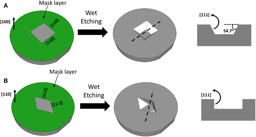
Figure 1. Wet anisotropically etched regions in (A) a [100]-oriented silicon substrate. The side walls are formed by stable [111] planes at an angle of 54.7° with respect to the wafer surface. (B) A [110]-oriented silicon substrate. The side walls are formed by stable [111] panes perpendicular to the wafer surface.
Figure 2 outlines the fabrication steps used in this work for realizing waveguides and grating couplers using anisotropic wet etching process. We used a [110]-oriented SOI substrate with 340-nm thick top silicon layer on 2-μm thick buried oxide (BOx). First, we covered the silicon top surface with 10-nm thick thermally grown SiO2 and deposited another 10-nm thick layer of Si3N4 using plasma-enhanced chemical vapor deposition (PECVD) system. This combination acts as a hard mask during the wet etching process. The substrate was then spin-coated with 30 nm thick hydrogen silsesquioxane (HSQ), a negative electron-beam (e-beam) resist. Using e-beam lithography, desired patterns were then written onto the HSQ layer. After developing the HSQ layer, the patterns were transferred to the hard mask Si3N4/SiO2 using a combination of dry [using reactive ion etching (RIE)] and wet etching (using HF) process. This approach was adopted to avoid any damage to the silicon surface, since the TMAH etching process does not commence if the silicon surface is damaged due to the dry etching process or in the presence of any native oxide. After etching of the hard mask, the sample was immersed in a 25% aqueous solution of TMAH at room temperature. To remove the hard mask after TMAH etching, we used a combination of dry and wet etching (using HF) processes. Finally, the waveguides were spin-coated with a 1-μm thick spin-on-glass (Fox-16, Dow Corning), which acts as an upper cladding for the waveguides. After curing at 400°C, Fox-16 has similar refractive index as the Box layer (Song et al., 2011).
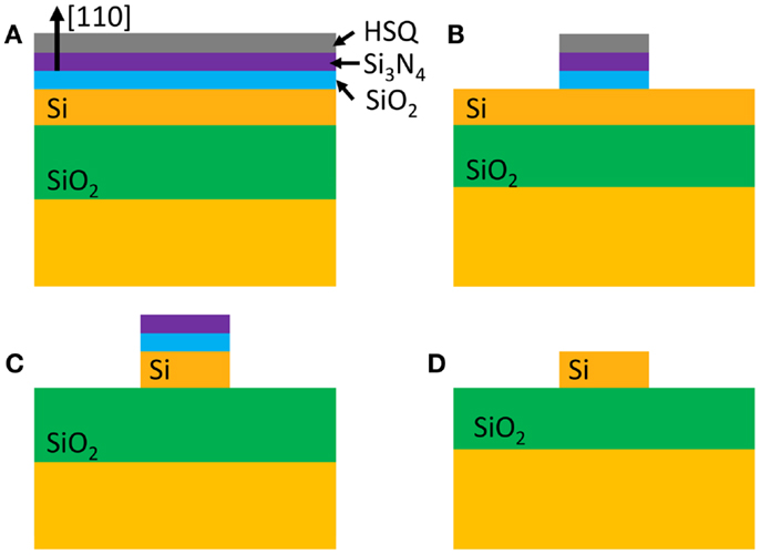
Figure 2. Anisotropic wet etching process: (A) A [110]-SOI substrate is covered with thin layers of SiO2, Si3N4, and HSQ. (B) Desired patterns are written in HSQ layer using e-beam lithography and then transferred to the hard mask (SiO2 and Si3N4) using dry and wet etching processes. (C) The patterns were transferred to the SOI using TMAH solution. (D) Finally, the hard mask was removed using a combination of dry and wet etching processes.
For comparison, we have also fabricated waveguides using standard dry etching process. We used the same substrate as used for wet etching process. The substrate was spin-coated with ZEP-520A resist, and waveguide patterns were written on to the resist using e-beam lithography. The patterns were then transferred to the silicon layer using inductively coupled plasma (ICP) etching process. The substrate was then treated in an O2 Plasma Asher to remove the resist before covering with 1-μm thick layer of Fox-16.
Figure 3A shows the remaining Si thickness as a function of etching time with an SEM cross-sectional view of the waveguides at different point of time. On an unpatterned SOI substrate, the etching rate was found to be 37 nm/min for the [110] direction, so that 340 nm thick top silicon layer was expected to be etched away in <10 min. However, for a patterned substrate, e.g., while fabricating waveguide structures, we found silicon residues at the bottom of the waveguide even after a long etching time [see inset (i) in Figure 3A]. This result indicates that the plane of the residual silicon, near the bottom of the waveguide, is semi-stable, and the etching rate is much slower than the Si [110] plane. Consequently, the substrates were overetched for 140 min to completely get rid of the residues [see inset (ii) in Figure 3A]. Interestingly, we did not observe any significant etching along the [111]-plane; in other words, the width of the waveguides remained almost unaltered during such prolonged etching process.
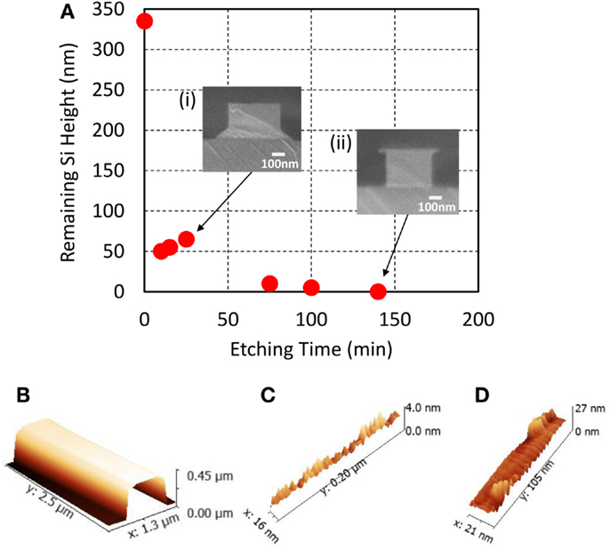
Figure 3. (A) Remaining silicon thickness as a function of time. Different patterned SOI samples were used to estimate the remaining Si height for different etching time. As one can notice initially the etch rate is quite fast, but at the end due to the presence of a semi-stable crystal plane, a long etch time was needed to completely remove the silicon around the waveguide. Inset (i) shows the waveguide cross-section with the presence of semi-stable plane after 10 min etching time. Inset (ii) shows the waveguide cross-section after 140 min of etching time. (B) AFM image of a silicon waveguide fabricated using wet etching process. (C) Close up view of the surface reveals a RMS roughness of 1.2 nm. (D) AFM image of a silicon waveguide fabricated using dry etching process with RMS roughness of 7 nm.
We also measured the roughness of the waveguide side walls using atomic force microscopy (AFM) and found that the surface of the silicon core is very smooth, as shown in Figure 3B. A more detailed AFM analysis (Figure 3C) reveals that the RMS roughness value was only 1.2 nm confirming minimal sidewall roughness, arising during the lithography and dry etching process of the hard mask, was transferred to the silicon layer. On the other hand, the RMS value of the side wall roughness was 7 nm, as shown in Figure 3D, for the waveguides fabricated by dry etching process.
Low-Loss Waveguides
To evaluate the propagating loss, we prepared straight waveguides with four different lengths ranging from 0.2 to 1.6 cm. The waveguide width was 380 nm, which supports only the fundamental transverse electric (TE) and transverse magnetic (TM) modes. A cut-back method was used to estimate the propagation loss of the waveguides. The waveguides were tested using a tunable laser source with a tuning range from 1520 to 1630 nm. In order to select different polarizations, we have used a fiber polarization controller. Light was launched and collected from the waveguides using a fiber coupler setup. The collected light was then sent to a photodetector, which automatically plots the output vs. wavelength.
We have measured the transmission of the waveguides with different lengths for both TE and TM polarizations and also different etching conditions. For each propagation length, we measured a set of five waveguides and considered the average value to estimate the propagation loss. This was done to avoid any unwanted variation in the coupling condition for different waveguides. According to the cut-back method, the propagation loss can be estimated from the slope of the fitted line. Figures 4A,B show the normalized transmission for TE and TM polarization, respectively, at 1550-nm wavelength. In both Figures 4A,B, the red squares represent the normalized transmission for wet etched waveguides and the black circles represent the normalized transmission for dry etched waveguides. The red and black lines represent the linear fits for the wet etched waveguide and dry etched waveguide data. To emphasize the effect of different etching techniques and polarizations on the propagation loss, waveguide transmissions were normalized by setting the background loss (which includes coupling loss and setup loss) to 0 dB. From Figure 4A, for TE polarization, the estimated propagation loss for the wet etched waveguide was only 0.85 dB/cm, which is significantly smaller than the propagation loss of 4.69 dB/cm for the dry etched waveguides. On the other hand, for TM polarization, the propagation losses are quite similar for wet-etched waveguides and dry-etched waveguides with 1.08 and 1.67 dB/cm, respectively, as shown in Figure 4B. It is important to mention here that the propagation loss for our dry etched waveguides is relatively higher than the previously reported results (Dumon et al., 2004; Bogaerts et al., 2005; Tsuchizawa et al., 2005, 2006; Gnan et al., 2008; Qiu et al., 2014).
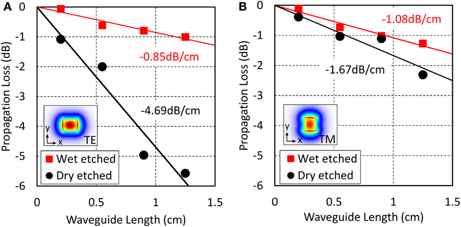
Figure 4. (A) TE polarization: normalized transmission of the fabricated waveguides using wet etching (red squares) and dry etching (black circles) techniques. The transmission of the wet etched and dry etched waveguides were normalized relative to −15.68 and −16.41 dB, respectively, which corresponds to the setup and grating coupler losses. (B) TM polarization: normalized transmission of the fabricated waveguides using wet etching (red squares) and dry etching (black circles) techniques. The transmission of the wet etched and dry etched waveguides were normalized relative to −20.78 and −20.67 dB, respectively. The insets show the mode profiles of the TE and TM modes. We measured the minimum propagation loss of 0.85 dB/cm for TE polarization and 1.08 dB/cm for TM polarization for wet etched waveguides.
For dry etched waveguides, TE modes tend to have more propagation loss than TM modes. This is due to the fact that while TM mode concentrates most of its energy along the top and bottom surface, TE mode, on the other hand, concentrates along the side walls. The two modes are shown in the insets of Figures 4A,B. Since dry etching tends to leave a rougher side wall, as it is apparent from Figure 3D, TE mode suffers more propagation loss than TM mode. However, in case of wet etching process, side wall roughness is considerably reduced and becomes comparable to the roughness of the top and bottom surface. Hence, the loss for TE and TM is almost the same in case of wet etched waveguides. This could be the first step for polarization-independent Si optical circuits.
Grating Coupler
Surface grating couplers are the most popular way to couple light between a high-index contrast silicon waveguide and a single mode optical fiber. The optical mode from the compact silicon waveguide is first expanded laterally along an adiabatically tapered waveguide and then redirected out-of-plane by the grating coupler toward the optical fiber, which is normally placed at a near-normal orientation over the grating coupler. The coupling efficiency of a grating coupler is decided by how well it directs light toward the optical fiber and how well the radiated field matches the Gaussian field profile of the fiber mode. Several grating coupler designs with high coupling efficiency have been previously proposed both using 1D line gratings (Taillaert et al., 2004; Cheben et al., 2006; Roelkens et al., 2008; Tang et al., 2010) and 2D subwavelength structures (Chen and Tsang, 2009; Halir et al., 2010).
While designing grating coupler for wet etching process, we have to consider the restrictions imposed by the wet etching process, since the crystal planes dictates the shape of the structures to be fabricated. For a [110]-oriented SOI wafer, only [112] and [11−2] directions give stable vertical side walls. Therefore, these two crystal directions were used to design the grating coupler and the associated waveguide. Since the angle between these two planes is 109.47°, a 1D grating is difficult to design. This is due to the fact that in a 1D grating coupler, the grooves need to be perpendicular to the direction of the waveguide for efficient coupling. Consequently, we opted for a 2D subwavelength grating design, as shown in Figure 5A. The optimized design parameters were determined with 3D finite-difference time domain (FDTD) method using Lumerical, a commercially available software. We have also linearly apodized the grating structure along the direction of light propagation to improve the coupling efficiency. Along x-direction, the periodicity was kept constant at ax = 350 nm with 30 rows of grooves. Along y-direction, the first 11 periods had periodicity of ay = 600 nm, and then the periodicity was linearly varied from 600 nm down to 550 nm over the next 11 periods to achieve apodization. The shape of the grooves, shown in Figure 5B, is a parallelogram with its longer arms along [11−2] direction, same as the waveguide, and the shorter arms along [112] direction. Along with the [111] planes perpendicular to [112] and [11−2] directions, there are other two [111] planes, at an angle of 35.3° with the [110] surface, which also decide the extent of the groove depth. The grooves in the uniform (unapodized) section are l = 430 nm long and w = 200 nm wide. In the apodized section, while the width was kept constant at w = 200 nm, the length was linearly varied from l = 430 to 270 nm. Finally, the length of the adiabatic waveguide taper required to create lossless transition between a 380-nm wide silicon waveguide and the 10-μm wide grating coupler was chosen to be 500 μm. Interestingly, in the fabricated device, we did not see any noticeable effect of the anisotropy of the wet etching process, this is probably because the deviation of the taper side wall from the [112] direction was below 1°.
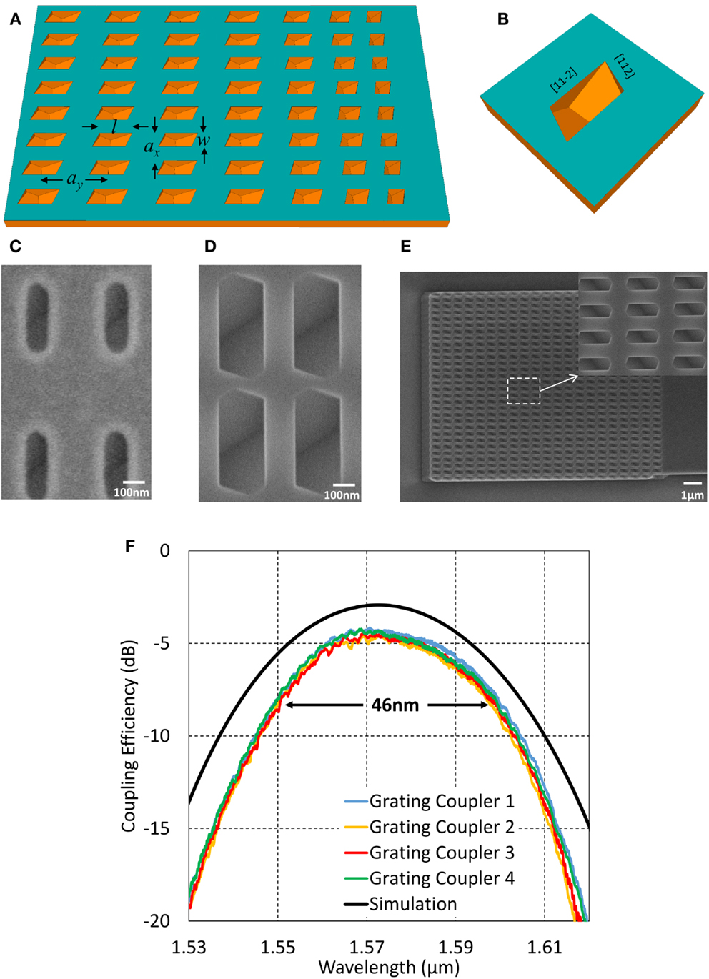
Figure 5. (A) Schematic image of the grating coupler. (B) Schematic of the groove initially considered for simulation. (C) SEM image of the hard mask showing rounded corners. (D) SEM image of the grooves of the fabricated grating showing their hexagonal shape, the intersection of two [111] planes is also visible inside the groove. (E) SEM image of the fabricated grating coupler with optimized design. (F) Simulated and measured spectral response of different grating couplers. The black curve shows the simulated coupling spectrum for the grating coupler. The remaining curves show the measured coupling spectra. The maximum coupling efficiency was −4.16 dB at 1570 nm and 3 dB bandwidth of 38 nm.
The grating couplers were fabricated simultaneously with the low-loss waveguides and using the same fabrication process as discussed in previous sections. Although the grooves were designed to have four sides only along [112] and [11−2] directions, due to proximity effect in the e-beam system, the corners of the openings on the hard mask was rounded, as shown in Figure 5C. For a [110]-oriented silicon substrate, along with [112] directions, [110] direction also produces stable planes, but at an angle of 35.3° with the surface. As a result, the fabricated grating had grooves with hexagonal shape, as shown in Figure 5D. Figure 5E shows the overall view of the fabricated grating coupler. The black curve in Figure 5F shows the simulated wavelength spectrum of the grating coupler for TE polarization, which predicts a maximum coupling efficiency of −2.9 dB around 1570 nm wavelength when the input fiber is tilted at an angle of 10° with respect to the surface normal. The measurement was performed by coupling light in and out of two grating couplers, connected by a silicon waveguide, with two single mode fibers both tilted at a specific angle relative to the surface normal of the grating couplers. The coupling efficiency of the individual grating coupler was then extracted from the overall insertion loss of the device after subtracting the loss due to the interconnecting waveguide. Four different spectra of the same grating coupler design are plotted. It can be seen that all the spectra closely coincide (with ~0.5 dB variation) demonstrating good repeatability in the fabrication process. The maximum efficiency was estimated to be −4.16 dB, deviating by 1.26 dB from the simulated efficiency, and the spectrum is centered on 1570 nm closely matching the simulated structure. However, the slight discrepancy between the simulation and the measured efficiency could have caused mainly due to accumulated fabrication errors, as controlling the exact position of the [110] sides of the grooves is difficult. The measured 3-dB bandwidth was about 46 nm in comparison to 48 nm as estimated from the simulation.
Conclusion and Future Work
In conclusion, we have proposed a novel and simple fabrication technique for realizing low-loss silicon waveguides and grating coupler using anisotropic wet etching technique. To realize vertical side walls of a waveguide, we used the [111] planes of a [110]-oriented SOI substrate. The AFM imaging shows a significant improvement in the side wall roughness of 1.2 nm for wet etched waveguides in comparison to 7 nm for dry etched waveguides. For TE polarization, we have achieved a propagation loss of only 0.85 dB/cm for wet etched waveguides. This is significantly smaller than the propagation loss of 4.69 dB/cm measured for dry etched waveguides. Besides, the propagation loss for TM polarization was 1.08 dB/cm, which suggests that this proposed wet etching process can be used to fabricate polarization-insensitive waveguide structures. We have also demonstrated an efficient grating coupler fabricated using the same wet etching technique. The grating coupler consists of grooves with hexagonal shape. The groove shape and depth are decided by the stable crystal planes along [111]. The measured coupling efficiency of the optimized grating coupler was found to be −4.3 dB at 1565 nm with 3 dB bandwidth of 38 nm.
Author Contributions
SS and GR conceived the idea. KD, HA, and AP performed the device design and simulation. KD, MH, and AA-A performed the fabrication. RP performed the AFM imaging. KD wrote the manuscript. All authors were involved in the analysis of the results and revision of the manuscript.
Conflict of Interest Statement
The authors declare that the research was conducted in the absence of any commercial or financial relationships that could be construed as a potential conflict of interest.
Acknowledgments
This work is supported by EPSRC Standard Grant (EP/M009416/1), EPSRC Manufacturing Fellowship (EP/M008975/1), EU FP7 Marie-Curie Carrier-Integration-Grant (PCIG13-GA-2013-618116), University of Southampton Zepler Institute Research Collaboration Stimulus Fund, and Hitachi. Data availability: All data supporting this study are available upon request from the University of Southampton repository at http://dx.doi.org/10.5258/SOTON/384541.
References
Bogaerts, W., Baets, R., Dumon, P., Wiaux, V., Beckx, S., Taillaert, D., et al. (2005). Nanophotonic waveguides in silicon-on-insulator fabricated with CMOS technology. J. Lightwave Technol. 23, 401–412. doi: 10.1109/JLT.2004.834471
Cardenas, J., Poitras, C. B., Robinson, J. T., Preston, K., Chen, L., and Lipson, M. (2009). Low loss etchless silicon photonic waveguides. Opt. Express 17, 4752–4757. doi:10.1364/OE.17.004752
Cheben, P., Janz, S., Xu, D.-X., Lamontagne, B., Delâge, A., and Tanev, S. (2006). A broad-band waveguide grating coupler with a subwavelength grating mirror. IEEE Photon. Technol. Lett. 18, 13–15. doi:10.1109/LPT.2005.860037
Chen, X., and Tsang, H. K. (2009). Nanoholes grating couplers for coupling between silicon-on-insulator waveguides and optical fibers. IEEE Photon. J. 1, 184–190. doi:10.1109/JPHOT.2009.2031685
Dumon, P., Bogaerts, W., Wiaux, V., Wouters, J., Beckx, S., Campenhout, J. V., et al. (2004). Low-loss SOI photonic wires and ring resonators fabricated with deep UV lithography. IEEE Photon. Technol. Lett. 16, 1328–1330. doi:10.1109/LPT.2004.826025
Fischer, U., Zinke, T., Kropp, J.-R., Arndt, F., and Petermann, K. (1996). 0.1 dB/cm waveguide losses in single mode SOI rib waveguides. IEEE Photon. Technol. Lett. 8, 647–648. doi:10.1109/68.491567
Gardes, F. Y., Reed, G. T., Knights, A. P., Mashanovich, G., Jessop, P. E., Rowe, L., et al. (2008). Sub-micron optical waveguides for silicon photonics formed via the local oxidation of silicon (LOCOS). Proc. SPIE 6898, 68980R. doi:10.1117/12.765383
Gnan, M., Thomas, S., Macintyre, D. S., De La Rue, R. M., and Sorel, M. (2008). Fabrication of low-loss photonic wires in silicon-on-insulator using hydrogen silsesquioxane electron-beam resist. Electron. Lett. 44, 115–116. doi:10.1049/el:20082985
Halir, R., Cheben, P., Schmid, J. H., Ma, R., Bedard, D., Janz, S., et al. (2010). Continuously apodized fiber-to-chip surface grating coupler with refractive index engineered subwavelength structure. Opt. Lett. 35, 3243–3245. doi:10.1364/OL.35.003243
Lee, K. K., Lim, D. R., and Kimerling, L. C. (2001). Fabrication of ultralow-loss Si/SiO2 waveguides by roughness reduction. Opt. Lett. 26, 1888–1890. doi:10.1364/OL.26.001888
Liu, Y. X., Hayashida, T., Matsukawa, T., Endo, K., O’uchi, S., Sakamoto, K., et al. (2008). “An experimental study of TiN gate finFET SRAM with (111)-oriented sidewall channels,” in IEEE Silicon Nanoelectronics Workshop (SNW) (Honolulu: IEEE), 1–2.
Miller, D. A. B. (2009). Device requirements for optical interconnects to silicon chips. Proc. IEEE 97, 1166–1185. doi:10.1109/JPROC.2009.2014298
Pafchek, R., Tummidi, R., Li, J., Webster, M. A., Chen, E., and Koch, T. L. (2009). Low-loss silicon-on-insulator shallow-ridge TE and TM waveguides formed using thermal oxidation. Appl. Opt. 48, 958–963. doi:10.1364/AO.48.000958
Qiu, C., Sheng, Z., Li, H., Liu, W., Li, L., Pang, A., et al. (2014). Fabrication, characterization and loss analysis of silicon nanowaveguides. J. Lightwave Technol. 32, 2303–2307. doi:10.1109/JLT.2014.2309122
Roelkens, G., Vermeulen, D., Thourhout, D. V., Baets, R., Brision, S., Lyan, P., et al. (2008). High efficiency diffractive grating couplers for interfacing a single mode optical fiber with a nanophotonic silicon-on-insulator waveguide circuit. Appl. Phys. Lett. 92, 131101. doi:10.1063/1.2905260
Rowe, L. K., Elsey, M., Tarr, N. G., Knights, A. P., and Post, E. (2007). CMOS-compatible optical rib waveguides defined by local oxidation of silicon. Electron. Lett. 43, 392–393. doi:10.1049/el:20073680
Schmidtchen, J., Splett, A., Schüppert, B., Petermann, K., and Burbach, G. (1991). Low loss singlemode optical waveguides with large cross-section in silicon-on-Insulator. Electron. Lett. 27, 1486–1488. doi:10.1049/el:19910930
Song, B.-S., Jeon, S.-W., and Noda, S. (2011). Symmetrically glass-clad photonic crystal nanocavities with ultrahigh quality factors. Opt. Lett. 36, 91–93. doi:10.1364/OL.36.000091
Suzuki, S., Yanagisawa, M., Hibino, Y., and Oda, K. (1994). High-density integrated planar lightwave circuits using SiO2-GeO2 waveguides with a high refractive index difference. J. Lightwave Technol. 12, 790–796. doi:10.1109/50.293970
Taillaert, D., Bienstman, P., and Baets, R. (2004). Compact efficient broadband grating coupler for silicon-on-insulator waveguides. Opt. Lett. 29, 2749–2751. doi:10.1364/OL.29.002749
Tang, Y., Wang, Z., Wosinski, L., Westergren, U., and He, S. (2010). Highly efficient nonuniform grating coupler for silicon-on-insulator nanophotonic circuits. Opt. Lett. 35, 1290–1292. doi:10.1364/OL.35.001290
Tsuchizawa, T., Yamada, K., Fukuda, H., Watanabe, T., Takahashi, J., Takahashi, M., et al. (2005). Microphotonics devices based on silicon microfabrication technology. IEEE J. Sel. Top. Quantum Electron. 11, 232–240. doi:10.1109/JSTQE.2004.841479
Keywords: silicon photonics, waveguide, anisotropic wet etching, grating coupler, integrated photonics
Citation: Debnath K, Arimoto H, Husain MK, Prasmusinto A, Al-Attili A, Petra R, Chong HMH, Reed GT and Saito S (2016) Low-Loss Silicon Waveguides and Grating Couplers Fabricated Using Anisotropic Wet Etching Technique. Front. Mater. 3:10. doi: 10.3389/fmats.2016.00010
Received: 15 December 2015; Accepted: 08 February 2016;
Published: 22 February 2016
Edited by:
Petra Granitzer, Karl-Franzens-University Graz, AustriaReviewed by:
Androula Galiouna Nassiopoulou, National Center for Scientific Research - Demokritos, GreeceKoji Yamada, National Institute of Advanced Industrial Science and Technology, Japan
Tatiana S. Perova, The University of Dublin, Ireland
Nobuyoshi Koshida, Tokyo University of Agriculture and Technology, Japan
Copyright: © 2016 Debnath, Arimoto, Husain, Prasmusinto, Al-Attili, Petra, Chong, Reed and Saito. This is an open-access article distributed under the terms of the Creative Commons Attribution License (CC BY). The use, distribution or reproduction in other forums is permitted, provided the original author(s) or licensor are credited and that the original publication in this journal is cited, in accordance with accepted academic practice. No use, distribution or reproduction is permitted which does not comply with these terms.
*Correspondence: Kapil Debnath, ay5kZWJuYXRoQHNvdG9uLmFjLnVr