 Guohai Chen
 Yenan Song
- 1Department of Physics and Astronomy, Brigham Young University, Provo, UT, USA
- 2Engineering Research Center for Nanophotonics and Advanced Instrument, Ministry of Education, School of Physics and Materials Science, East China Normal University, Shanghai, China
A field emission from a lateral emitter made by a multiwalled carbon nanotube (MWCNT) yarn was investigated. The lateral emitter showed an excellent field emission performance with a low turn-on electric field of 1.13 V/μm at an emission current of 1 μA, high emission current of 0.2 mA at an applied voltage of 700 V, and longtime emission stability for over 20 h without any significant current decay under an initial emission current of about 0.10 mA. The lateral emitter also demonstrated a uniform line emission pattern. It is suggested that the field emission occurs from the outmost MWCNTs that are protruding out from the yarn surface.
Introduction
Due to the unique properties as field emitters, such as high field enhancement factor, good mechanical strength, and excellent chemical stability, carbon nanotubes (CNTs) have been considered as one of the next-generation cold cathode materials for applications of field emission displays, lamps, X-ray sources, high-resolution electron-beam instruments, and microwave amplifiers, etc. (Lee et al., 1999; Saito and Uemura, 2000; Kim et al., 2015; Lei et al., 2015). Various techniques have been studied to fabricate CNT emitters using as-grown, spraying, electrophoresis, and screen-printing methods, etc. (Choi et al., 1999; She et al., 2003; Jeong et al., 2006; Jung et al., 2006; Chen et al., 2008, 2013; Song et al., 2016). These techniques have mainly focused on field emission from a vertical configuration, i.e., field emission from the tip of CNTs (Jung et al., 2006; Chen et al., 2009, 2012). However, simulation studies have shown that the lateral field emission is possible as well, in which electrons emit predominately not from the tip of CNTs but from the body of CNTs (Zhou and Kawazoe, 2001; Zhou et al., 2001). Experimentally, an individual loop-shaped CNT was studied to explain electron emission from the side wall of the CNT (Konishi et al., 2005; Chai and Chow, 2007). In addition, another study using the CNT loop arrays showed that the efficient emission occurred at the loop apex (Futaba et al., 2012). Furthermore, it has also been demonstrated that horizontally aligned CNT emitters were considerably more stable and uniform than vertically aligned CNT emitters (Jung et al., 2007a). CNT yarns/fibers, as one of the most promising CNT assemblies, have attracted extensive attention. Field emission properties from vertical configuration of yarns/fibers, using various fabrication methods, have been investigated (Wei et al., 2008; Chen et al., 2009; Jang et al., 2010; Hojati-Talemi et al., 2013; Fairchild et al., 2015). A study of field emission from the side of CNT yarn showed a similar performance to the tip of yarn induced in a scanning electron microscope, demonstrating that the field emission from lateral configuration is promising as well (Jang et al., 2010). However, the previous studies have showed that the fabrication methods of CNT emitters were relatively complicated. It is still challenging to fabricate lateral field emission emitters using relatively simple approaches.
Here, we demonstrated field emission from a lateral multiwalled carbon nanotube (MWCNT) yarn emitter which can be easily handled with hands. The lateral emitter presented an emission current of 0.2 mA at applied voltage of 700 V and an emission stability for over 20 h without any significant current decay under an initial emission current of about 0.10 mA. It is suggested that the field emission occurred from the outmost MWCNTs which were protruding out from the yarn surface. A uniform line emission pattern was achieved, suggesting that this lateral emitter can be used for lamps, figure display boards, cylindrical cathodes, etc.
Experimental
Preparation of Yarns
The MWCNT yarn can be made out of super-aligned MWCNTs using a spinning technique (Jiang et al., 2002; Zhang et al., 2006). The yarns were obtained from Tsinghua University, Beijing, China. The pristine MWCNT yarn was pulled through an ethylene glycol solvent (purchased from Sigma-Aldrich) to make it stiffer and packed tighter. Then a thermal treatment at 200–250°C for 30 min in air in a forced convection oven (JEIO TECH OF-22GW) was conducted to completely evaporate the solvent. The morphology of the yarn was characterized by scanning electron microscopy (SEM, Hitachi, S-4700).
Fabrication of Lateral Yarn Emitters
Since the MWCNT yarn has a macroscopic dimension, it can be easily manipulated by hand. A schematic diagram of the lateral MWCNT yarn emitter is shown in Figure 1. A nearly 20 mm-long yarn was attached on a stainless steel support using a conducting epoxy (silver paste, purchased from MG Chemicals). A simple manipulation system is enough to attach the yarn on the support because the segment of the yarn can be handled easily using tweezers. Thus, the fabrication of CNT emitters is very simple and easy. The sample was put in the oven to subject a thermal annealing under atmosphere pressure at 80°C for 15 min, which can enhance the mechanical adhesion between the yarn and the support. Finally, the sample was put in a vacuum chamber at a pressure less than 2 × 10⁻⁷ torr to investigate field emission properties. Field emission measurements were carried out using a diode configuration. The anode was a homemade phosphor-coated indium tin oxide (ITO) glass with a width of ~10 mm. The phosphor powder and binder were purchased from Alibaba and then screen-printed on ITO-coated glass (purchased from Sigma-Aldrich). The gap between the anode and the yarn was adjusted to 400 μm by ceramic spacers. The emission current was monitored with a Keithley 6485, and the direct current power was supplied by a constant power voltage and current controller (HCN140-3500).
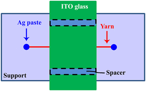
Figure 1. Schematic diagram of the diode configuration for field emission measurements.
Results and Discussion
Morphology of the Yarn
Figure 2A shows a SEM image of the MWCNT yarn with low magnification. The diameter of the MWCNT yarn is about 50 μm. It is obvious that the surface of the MWCNT yarn is very smooth and even. We observed the yarn throughout the entire length and could not find noticeable protruding CNT tips on the surface at this magnification. This indicates that MWCNTs are tightly bound together within the yarn. The high magnification SEM images are shown in Figures 2B,C. The yarn consists of arrays of aligned MWCNTs, but some of MWCNTs show the curly shape. The two ends (tips) of the curly CNTs are just buried under the neighboring CNTs. Figure 2D shows the highly magnified SEM image of the yarn surface. There are many outmost MWCNTs protruding out from the yarn surface, indicated by the white arrows. An exaggerated example was also presented in the inset of Figure 2D. It is worth noting that most of the protruding CNTs are not so far away from the surface. This typical microstructure can allow field emission possible from the MWCNT yarn.
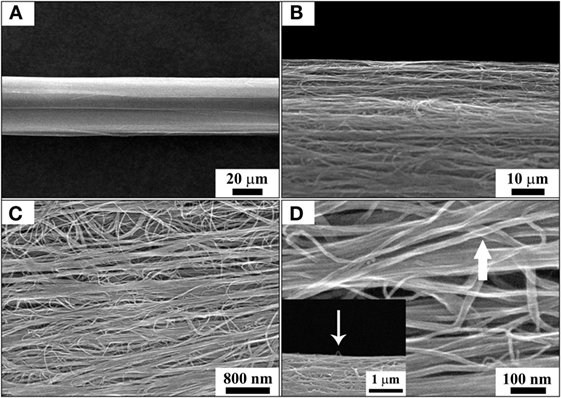
Figure 2. SEM images of the MWCNT yarn with (A) low and (B–D) high magnifications. The white arrows in (D) indicate the outmost MWCNTs protruding out from the yarn surface.
Field Emission Characteristics
We investigated field emission properties of the lateral MWCNT yarn emitter. A strong uniform line emission pattern was observed from the lateral emitter, as shown in Figure 3A. The two joints were kept uncovered by the ITO glass to avoid field emission from the silver paste (Ag paste) or other potential undesirable parts. It clearly reveals that the field emission is from the lateral emitter. This uniform line emission pattern can be used for lamps, figure display boards, cylindrical cathodes, etc.
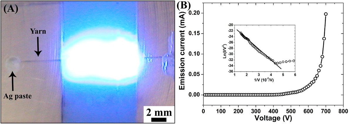
Figure 3. (A) A strong line emission pattern with a length of about 10 mm. (B) Field emission characteristics of the lateral emitter. The inset shows the corresponding F–N plot.
Field emission characteristics of the lateral emitter are shown in Figure 3B. The lateral emitter demonstrated excellent field emission performance with a turn-on electric field of 1.13 V/μm at an emission current of 1 μA and an emission current of 0.2 mA at an applied voltage of 700 V. It was assumed that the field emission occurred from the top half of the yarn surface. Based on the diameter of the yarn (50 μm) and the length (10 mm), the corresponding emission current density was calculated as ~25.5 mA/cm2. This current level is enough for field emission display applications. The lateral emitter exhibited a better or comparable field emission performance in comparison with other reported lateral emitters or vertical emitters (Gao et al., 2001; Jo et al., 2003; Seelaboyina et al., 2006; Jang et al., 2010; Chen et al., 2013). For example, the electron emission threshold for a current density of 1 mA/cm2 was 4 and 6.5 V/μm for the single-walled CNT film prepared using methanol and DMF, respectively, with the gap distance of 165 μm and emission area of 6 mm2 (Gao et al., 2001). It means that the emitters reached 60 μA at the voltage of 660 or 1072 V. In addition, the values of electric field required to obtain a current density of 1 mA/cm2 were in the range of 5.40–12.8 V/μm for samples with different CNT lengths and number densities, with a gap distance of 300 μm, an emission size of 5-mm diameter, and the maximum emission current density is about 2.2 mA/cm2 (Jo et al., 2003). It implies that the emitters reached about 0.2 mA at the voltage range of 1620–3840 V. Furthermore, the thin MWCNTs reached the maximum emission current of less than 0.2 mA at an applied voltage of 1500 V with a gap distance of 380 μm (Seelaboyina et al., 2006). The low turn-on electric field and relatively high current (and current density) at low applied voltage suggested a better field emission performance of our lateral emitter compared to these reports. The inset in Figure 3B shows the corresponding Fowler–Nordheim (F–N) plot. The straight line indicates the quantum mechanical tunneling characteristic of field electron emission. The field enhancement factor can be calculated using the F–N equation:
where I is the emission current, A = 1.56 × 10⁻⁶ AV−2 eV, B = 6.83 × 10⁹ eV−3/2 Vm−1, α is the effective emission area, β is the field enhancement factor, φ is the work function, V is the applied voltage, and d is the gap distance between the anode and the emitter. Using Eq. 1, the slope of the F–N plot [log(I/V2) versus 1/V] is given by:
Therefore, the field enhancement factor can be calculated from the F–N plot assuming the work function of the MWCNTs to be 5.0 eV (de Jonge et al., 2004). The field enhancement factor of our lateral emitter is 8300. This large field enhancement factor indicates that the lateral emitter can start to emit electrons at a considerably low applied voltage.
Field emission stability is one of the important parameters for practical applications of CNT-based field emission cold cathodes. We evaluated emission current stability of the lateral emitter at an initial emission current of about 0.10 mA under a direct current bias. Then, the applied voltage was kept constant for over 20 h. As a matter of fact, this initial current is strong enough to perform acceleration test for field emission stability (the corresponding current density is about 12.7 mA/cm2) compared with the previous reports (Moon et al., 2006; Jung et al., 2007a). As shown in Figure 4, the lateral emitter showed a very stable emission current for over 20 h without any significant current decay, indicating a better field emission stability (Moon et al., 2006; Jung et al., 2007b). The excellent field emission stability is mainly attributed to the tight bonding of neighboring MWCNTs within the yarn. The yarn was densified and shrank into a tight structure with several tens of micrometers in diameter after ethylene glycol treatment. The tightly bound MWCNT yarn would not easily degrade as applying high electric field on it. As a result, the lateral emitter demonstrated a long-term emission stability.
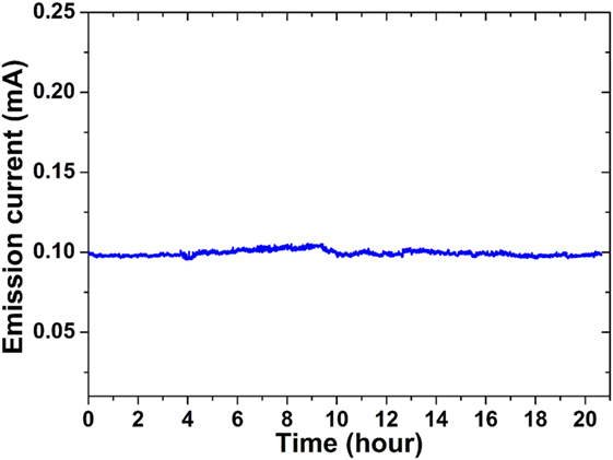
Figure 4. Field emission stability without any significant decay for over 20 h at an initial current of ~0.10 mA.
The surface morphology of the lateral emitter after field emission measurement was observed as well. There was no noticeable damage to the surface of the MWCNT yarn after field emission stability test. In addition, most importantly, no protruding CNT tips were found. When we consider the morphology of the yarn, some outmost MWCNTs protrude out from the surface, as shown in Figure 2D. They look just like CNT loops in other reports (Konishi et al., 2005; Futaba et al., 2012). Electrons can be easily extracted out from these protruding MWCNTs due to the concentrated electric field compared with other MWCNTs inside the yarn. Literature survey shows that field emission can either from the tip of CNTs or even from the body of CNTs (Zhou and Kawazoe, 2001; Zhou et al., 2001; Konishi et al., 2005). Here, it is suggested that the field emission occurs from the outmost MWCNTs which are protruding from the yarn surface. When the electrical bias is applied, the electric field is concentrated on the surface of the yarn, especially on the outmost MWCNTs which are protruding from the surface. This phenomenon is similar to the concentrated electric field at the protruding tips of the vertically aligned CNTs. The lateral yarn emitter showed high emission current, long-term emission stability, and uniform line emission pattern, suggesting its potential field emission applications such as line-shaped emitters, figure display boards, and cylindrical lamps.
We also investigated the field emission properties as a function of the gap between the anode and the lateral emitter. The same lateral MWCNT yarn emitter was used to study the gap dependence. The gap was adjusted as 100, 200, 400, 600, and 800 μm, separately, by ceramic spacers. The emission current–applied voltage (I − V) curves of the lateral emitter as a function of the gap are shown in Figure 5. It can be seen that the I − V curves shift to the right (higher voltage) as increasing the gap. The turn-on electric field was 2.30 V/μm for the gap of 100 μm. As the gap was increased to 200 μm, the turn-on electric field dramatically decreased to 1.46 V/μm. Continuous increasing of the gap to 400, 600, and 800 μm resulted in the turn-on field of 1.13, 1.11, and 0.96 V/μm, respectively. These values indicate lower turn-on electric fields than those of the vertical emitters. The lateral emitter shows a same gap dependence of field emission properties as the conventional vertical emitters (Choi et al., 2000; Moon et al., 2006; Chen et al., 2009).
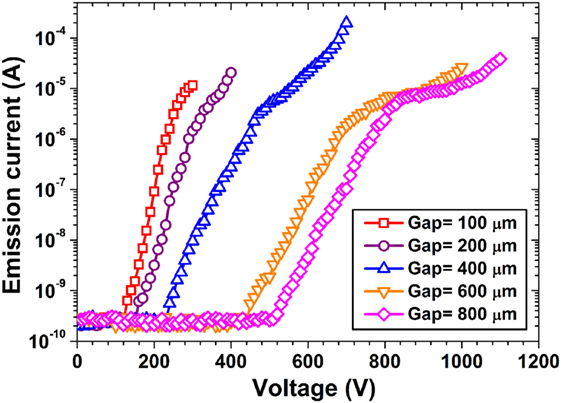
Figure 5. I − V curves of the lateral emitter as a function of the gap between the anode and the emitter.
Some potential applications of our lateral emitter are demonstrated in Figure 6. First, a field emission cylindrical lamp based on the lateral emitter is presented in Figure 6A. A phosphor-coated flexible transparent film can be easily made and used as the anode, and therefore a cylindrical lamp can be assembled without using hardly fabricated uniform flexible emission cathode. Second, a figure display board is also possible using our line-shaped emitter (Figure 6B). A patterned phosphor-coated ITO glass can be used as the anode. The spacers are used not only to separate the anode and the emitter but also to isolate the influence from other MWCNT yarns nearby. It is worth noting that the specifications need to be evaluated once the real device is made, such as power assumption, output luminosity as in reference (Croci et al., 2004).
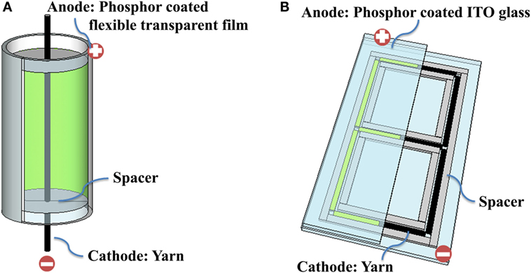
Figure 6. Schematic diagrams of potential applications of lateral field emitters with (A) cylindrical lamp and (B) display board.
Conclusion
An efficient lateral field emitter was simply fabricated using a MWCNT yarn, and its field emission properties were investigated. The lateral emitter exhibited excellent field emission properties with high emission current, longtime emission stability, and uniform line emission pattern. It is considered that the outmost MWCNTs which are protruding out from the yarn surface contributed to the field emission. The lateral emitter is promising as used in various field emission devices.
Author Contributions
GC designed and conducted the experimental, and both authors wrote the manuscript.
Conflict of Interest Statement
The authors declare that the research was conducted in the absence of any commercial or financial relationships that could be construed as a potential conflict of interest.
Acknowledgments
This work was partially supported by the Scientific Research Foundation for the Returned Overseas Chinese Scholars, Ministry of Education, China.
References
Chai, G. Y., and Chow, L. (2007). Electron emission from the side wall of an individual multiwall carbon nanotube. Carbon N. Y. 45, 281–284. doi:10.1016/j.carbon.2006.09.030
Chen, G. H., Neupane, S., and Li, W. Z. (2012). Electron field emission properties of vertically aligned carbon nanotube point emitters. Diamond Relat. Mater. 25, 134–138. doi:10.1016/j.diamond.2012.03.002
Chen, G. H., Neupane, S., Li, W. Z., Chen, L. N., and Zhang, J. D. (2013). An increase in the field emission from vertically aligned multiwalled carbon nanotubes caused by NH3 plasma treatment. Carbon N. Y. 52, 468–475. doi:10.1016/j.carbon.2012.09.058
Chen, G. H., Shin, D. H., Iwasaki, T., Kawarada, H., and Lee, C. J. (2008). Enhanced field emission properties of vertically aligned double-walled carbon nanotube arrays. Nanotechnology 19, 415703. doi:10.1088/0957-4484/19/41/415703
Chen, G. H., Shin, D. H., Roth, S., and Lee, C. J. (2009). Field emission characteristics of point emitters fabricated by a multiwalled carbon nanotube yarn. Nanotechnology 20, 315201. doi:10.1088/0957-4484/20/31/315201
Choi, W. B., Chung, D. S., Kang, J. H., Kim, H. Y., Jin, Y. W., Han, I. T., et al. (1999). Fully sealed, high-brightness carbon-nanotube field-emission display. Appl. Phys. Lett. 75, 3129–3131. doi:10.1063/1.125253
Choi, Y. C., Shin, Y. M., Lim, S. C., Bae, D. J., Lee, Y. H., Lee, B. S., et al. (2000). Effect of surface morphology of Ni thin film on the growth of aligned carbon nanotubes by microwave plasma-enhanced chemical vapor deposition. J. Appl. Phys. 88, 4898–4903. doi:10.1063/1.1314614
Croci, M., Arfaoui, I., Stöckli, T., Chatelain, A., and Bonard, J.-M. (2004). A fully sealed luminescent tube based on carbon nanotube field emission. Microelectron. J. 35, 329–336. doi:10.1016/j.mejo.2003.07.003
de Jonge, N., Allioux, M., Doytcheva, M., Kaiser, M., Teo, K. B. K., Lacerda, R. G., et al. (2004). Characterization of the field emission properties of individual thin carbon nanotubes. Appl. Phys. Lett. 85, 1607–1609. doi:10.1063/1.1786634
Fairchild, S. B., Boeckl, J., Back, T. C., Ferguson, J. B., Koerner, H., Murray, P. T., et al. (2015). Morphology dependent field emission of acid-spun carbon nanotube fibers. Nanotechnology 26, 105706. doi:10.1088/0957-4484/26/10/105706
Futaba, D. N., Kimura, H., Zhao, B., Yamada, T., Kurachi, H., Uemura, S., et al. (2012). Carbon nanotube loop arrays for low-operational power, high uniformity field emission with long-term stability. Carbon N. Y. 50, 2796–2803. doi:10.1016/j.carbon.2012.02.043
Gao, B., Yue, G. Z., Qiu, Q., Cheng, Y., Shimoda, H., Fleming, L., et al. (2001). Fabrication and electron field emission properties of carbon nanotube films by electrophoretic deposition. Adv. Mater. 13, 1770–1773. doi:10.1002/1521-4095(200112)13:23<1770:AID-ADMA1770>3.0.CO;2-G
Hojati-Talemi, P., Hawkins, S., Huynh, C., and Simon, G. P. (2013). Understanding parameters affecting field emission properties of directly spinnable carbon nanotube webs. Carbon N. Y. 57, 388–394. doi:10.1016/j.carbon.2013.01.088
Jang, H. S., Jeon, S. K., and Nahm, S. H. (2010). Field emission properties from the tip and side of multi-walled carbon nanotube yarns. Carbon N. Y. 48, 4019–4023. doi:10.1016/j.carbon.2010.07.006
Jeong, H. J., Choi, H. K., Kim, G. Y., Il Song, Y., Tong, Y., Lim, S. C., et al. (2006). Fabrication of efficient field emitters with thin multiwalled carbon nanotubes using spray method. Carbon N. Y. 44, 2689–2693. doi:10.1016/j.carbon.2006.04.009
Jiang, K. L., Li, Q. Q., and Fan, S. S. (2002). Nanotechnology: spinning continuous carbon nanotube yarns – carbon nanotubes weave their way into a range of imaginative macroscopic applications. Nature 419, 801. doi:10.1038/419801a
Jo, S. H., Tu, Y., Huang, Z. P., Carnahan, D. L., Wang, D. Z., and Ren, Z. F. (2003). Effect of length and spacing of vertically aligned carbon nanotubes on field emission properties. Appl. Phys. Lett. 82, 3520–3522. doi:10.1063/1.1576310
Jung, S. I., Choi, J. S., Shim, H. C., Kim, S., Jo, S. H., and Lee, C. J. (2006). Fabrication of probe-typed carbon nanotube point emitters. Appl. Phys. Lett. 89, 233108. doi:10.1063/1.2402222
Jung, S. M., Jung, H. Y., and Suh, J. S. (2007a). Horizontally aligned carbon nanotube field emitters having a long term stability. Carbon N. Y. 45, 2917–2921. doi:10.1016/j.carbon.2007.10.002
Jung, S. I., Jo, S. H., Moon, H. S., Kim, J. M., Zang, D. S., and Lee, C. J. (2007b). Improved crystallinity of double-walled carbon nanotubes after a high-temperature thermal annealing and their enhanced field emission properties. J. Phys. Chem. C 111, 4175–4179. doi:10.1021/Jp0676078
Kim, Y. C., Park, S. H., Lee, C. S., Chung, T. W., Cho, E., Chung, D. S., et al. (2015). A 46-inch diagonal carbon nanotube field emission backlight for liquid crystal display. Carbon N. Y. 91, 304–310. doi:10.1016/j.carbon.2015.04.093
Konishi, Y., Hokushin, S., Tanaka, H., Pan, L. J., Akita, S., and Nakayama, Y. (2005). Comparison of field emissions from side wall and tip of an individual carbon nanotube. Jpn. J. Appl. Phys. 44, 1648–1651. doi:10.1143/Jjap.44.1648
Lee, C. J., Kim, D. W., Lee, T. J., Choi, Y. C., Park, Y. S., Lee, Y. H., et al. (1999). Synthesis of aligned carbon nanotubes using thermal chemical vapor deposition. Chem. Phys. Lett. 312, 461–468. doi:10.1016/S0009-2614(99)01074-X
Lei, W., Zhu, Z. Y., Liu, C. Y., Zhang, X. B., Wang, B. P., and Nathan, A. (2015). High-current field-emission of carbon nanotubes and its application as a fast-imaging X-ray source. Carbon N. Y. 94, 687–693. doi:10.1016/j.carbon.2015.07.044
Moon, J. S., Alegaonkar, P. S., Han, J. H., Lee, T. Y., Yoo, J. B., and Kim, J. M. (2006). Enhanced field emission properties of thin-multiwalled carbon nanotubes: role of SiOx coating. J. Appl. Phys. 100, 104303. doi:10.1063/1.2384795
Saito, Y., and Uemura, S. (2000). Field emission from carbon nanotubes and its application to electron sources. Carbon N. Y. 38, 169–182. doi:10.1016/S0008-6223(99)00139-6
Seelaboyina, R., Huang, J., and Choi, W. B. (2006). Enhanced field emission of thin multiwall carbon nanotubes by electron multiplication from microchannel plate. Appl. Phys. Lett. 88, 194104. doi:10.1063/1.2203218
She, J. C., Xu, N. S., Deng, S. Z., Chen, J., Bishop, H., Huq, S. E., et al. (2003). Vacuum breakdown of carbon-nanotube field emitters on a silicon tip. Appl. Phys. Lett. 83, 2671–2673. doi:10.1063/1.1614437
Song, M., Xu, P., Han, L. J., Yi, L., Wang, X., Li, Z. H., et al. (2016). Enhanced field-emission performance from carbon nanotube emitters on nickel foam cathodes. J. Electron. Mater. 45, 2299–2304. doi:10.1007/s11664-015-4308-1
Wei, Y., Liu, L., Liu, P., Xiao, L., Jiang, K. L., and Fan, S. S. (2008). Scaled fabrication of single-nanotube-tipped ends from carbon nanotube micro-yarns and their field emission applications. Nanotechnology 19, 475707. doi:10.1088/0957-4484/19/47/475707
Zhang, X. B., Jiang, K. L., Teng, C., Liu, P., Zhang, L., Kong, J., et al. (2006). Spinning and processing continuous yarns from 4-inch wafer scale super-aligned carbon nanotube arrays. Adv. Mater. 18, 1505–1510. doi:10.1002/adma.200502528
Zhou, G., Duan, W. H., and Gu, B. L. (2001). Dimensional effects on field emission properties of the body for single-walled carbon nanotube. Appl. Phys. Lett. 79, 836–838. doi:10.1063/1.1388871
Keywords: carbon nanotube, yarn, field emission, lateral emitter, field emission display
Citation: Chen G and Song Y (2016) Field Emission from Lateral Multiwalled Carbon Nanotube Yarn Emitters. Front. Mater. 3:48. doi: 10.3389/fmats.2016.00048
Received: 22 June 2016; Accepted: 11 October 2016;
Published: 26 October 2016
Edited by:
Marco Rossi, Sapienza University of Rome, ItalyReviewed by:
Imad Arfaoui, Pierre-and-Marie-Curie University, FranceAlberto Ansaldo, Fondazione Istituto Italiano di Technologia, Italy
Maurizio De Crescenzi, University of Rome “Tor Vergata”, Italy
Copyright: © 2016 Chen and Song. This is an open-access article distributed under the terms of the Creative Commons Attribution License (CC BY). The use, distribution or reproduction in other forums is permitted, provided the original author(s) or licensor are credited and that the original publication in this journal is cited, in accordance with accepted academic practice. No use, distribution or reproduction is permitted which does not comply with these terms.
*Correspondence: Guohai Chen, Z3VvaGFpY2hlbkBnbWFpbC5jb20=;
Yenan Song, c29uZ3llbmFuQDE2My5jb20=
†Present address: Guohai Chen, Department of Physics and Astronomy, Brigham Young University, Provo, UT, USA