 Kyriaki Tsirka
 Antigoni Katsiki
 Nikolaos Chalmpes
 Dimitrios Gournis
 Alkiviadis S. Paipetis
- 1Composite and Smart Materials Laboratory, Department of Materials Science and Engineering, University of Ioannina, Ioannina, Greece
- 2Department of Materials and Chemistry (Physical Chemistry and Polymer Science), Vrije Universiteit Brussel, Brussels, Belgium
- 3Layered and Nanoporous Materials Group, Laboratory of Ceramics and Composites, Department of Materials Science and Engineering, University of Ioannina, Ioannina, Greece
Graphene has outstanding properties that make it an auspicious material for many applications. This work presents the production of graphene oxide (GO) via the Langmuir—Blodgett process and the subsequent restoration of single layer graphene flakes (SLGF) via the chemical reduction, and thermal annealing of the GO. Scanning electron microscopy (SEM) and optical images were used to evaluate the morphology and surface coverage of the substrate with GO flakes. Through this technique, smooth dispersion, controllable development, and population of the GO single flakes on the Si substrate without size limitation have been achieved. The height distribution of the GO was monitored after each processing step by AFM measurements. Additionally, the effects of each process on the structure of the samples was systematically studied via 2D Laser Raman spectroscopy (LRS) mapping. The determination of the layer number on each graphene flake was accomplished by monitoring the observed Raman shifts as a function of the position and confirmed via AFM measurements. The spectroscopic analysis of the single flakes was performed in order to study their topography and identify their quality as a function of the processing steps. Via the topographic 2D analysis of both the first- and second-order vibrational modes as a function of the position on the crystal, the degree of graphitization and/or the presence of defects, as well as the presence of internal stresses were mapped. Such a systematic determination of the effects of reduction and annealing on the structure of single layer graphene from reduced GO produced via the Langmuir—Blodgett process is reported for the first time in literature.
Introduction
Graphene might be one of the most researched materials during the last decade. The unprecedented electronic (Geim and Novoselov, 2007), mechanical (Papageorgiou et al., 2017), thermal (Pop et al., 2012), and optical (Binder, 2017) properties of graphene have already been well documented in the literature. Its various uses, especially in electronics, have attracted notable scientific attention, particularly regarding the physics governing this unique material (Aoki and Dresselhaus, 2014). Additionally, the production methods for graphene have also been the object of considerable research efforts as the market of graphene continues to grow rapidly along with numerous patent filings (Intellectual Property Office GOV.UK, 2015). There exists more than 10 methods for graphene preparation with their main differences encountered in the precursor material and in the quantity, the quality, and the size of the produced crystals (Avouris and Dimitrakopoulos, 2012). Graphene production methods are generally categorized in top-down and bottom-up approaches (Bhuyan et al., 2016) and include mechanical exfoliation, chemical exfoliation, chemical synthesis, epitaxial growth, and chemical vapor deposition (CVD) (Bonaccorso et al., 2012).
The production method is intrinsically linked to the purity of the produced graphene which is crucial for targeted applications, especially in electronics. At the same time, not all methods are appropriate for producing relatively large single graphene crystals. The Langmuir—Blodgett technique offers the method for deposition of GO (relatively packed) on a desired substrate. This technique involves the creation and transfer of a monolayer thick film formed at the air-water interface. The formation of a monolayer at an air-water interface was mainly studied by Langmuir, while the deposition of such a film was extensively investigated by Blodgett (vertical dipping), who collaborated with Langmuir (Gengler, 2010). The process requires the use of a surfactant, normally a long chain molecule with amphiphilic behavior, the role of which is to force the molecules to spread all over the available surface area. Then, surface tension is applied until a solid film is formed on the desired substrate, as the substrate emerges from the liquid (Gengler, 2010). Following the aforementioned process, graphene oxide (GO) thin single crystals may be deposited onto practically any substrate, e.g., Si wafers. Subsequently, a reduction step is required in a chemical reducing agent, e.g., a solution of NaBH4. The resulting reduced graphene oxide (rGO) still contains a considerable amount of heteroatoms and defects, and thus further thermal treatment is required for removing them. Typical thermal treatment includes annealing. In the current study, an additional “healing” step is proposed for cleaning the graphene surface from undesired defects. This step is presented in the materials and methods part in detail.
Raman spectroscopy provides the ideal tool for the study of graphene. The ideal structure of the graphene lattice allows for the monitoring of any structural or chemical change in its structure via the monitoring of its Raman vibrational modes. Extended research has been reported in literature in relation to Raman studies of graphene and GO (Dresselhaus et al., 2008; Ferrari and Basko, 2013; Bokobza et al., 2014). Especially with regards to the annealing process of the GO, numerous studies have evaluated the effects of the temperature and the annealing environment both for mechanically exfoliated and CVD grown graphene (Lin et al., 2012; Botcha et al., 2014; Alyobi et al., 2017; Zion et al., 2017).
Xueshen et al. (2013) have studied the effects of thermal annealing in monolayer graphene obtained by mechanical exfoliation with scotch tapes. They utilized Raman spectroscopy and AFM microscopy in order to evaluate the tape residues, which should be removed, and the flattening of the edges of graphene. They reported that both the 2D peak and the G peak presented a blueshift in the annealed, under N2/H2 at 400°C and 5 mbar pressure, graphene. They also found an increase in the full width at half maximum (FWHM) of the 2D peak and a decrease in the intensity ratio of the 2D peak to the G peak. Annealing in this case led to the complete attachment of the edges of graphene to the surface of the substrate (SiO2). Ajlani et al. (2016) performed a qualitative evaluation of the effects of strain and doping in CVD-grown incommensurate twisted bilayer graphene (BG) before and after annealing at 1,050°C. Following a detailed analysis of the various peaks encountered in the case of BG, they reported that each graphene layer had a different response to strain and doping. The layer in contact with the SiO2 substrate was principally affected by strain, whereas the upper layer was principally affected by doping.
As mentioned earlier, numerous experimental studies have dealt with the characteristics of GO produced by various methods, as well the restoration of graphene from GO. However, to our knowledge, an experimental protocol regarding the effects of each process on the same GO samples produced via the Langmuir—Blodgett technique has not as yet been reported. This research effort addresses the production of single layer GO and the subsequent restoration of single layer graphene through via a purposely designed experimental protocol. An extensive Raman analysis for all process steps is presented in order to provide insight on the effects of commonly used procedures for GO restored graphene on the vibrational response of the material.
In more detail, single and bilayer flakes of GO supported onto Si wafers were produced using the Langmuir-Blodgett method. A series of controlled processes were subsequently applied on the surface of the flakes in order to eliminate the present defects and functional groups. These processing steps consisted of (i) the reduction of the GO in a reducing agent for the elimination of functional moieties (rGO), (ii) the thermal annealing of the reduced GO under inert atmosphere and elevated temperature for the further elimination of the defects and the relief of the stresses from the graphitic lattice (a-G), (iii) the “healing” of the defects (e.g., vacancies in the lattice) of the graphene sheets (h-G) via the chemical vapor deposition of acetylene, and finally (iv) a second thermal annealing of the graphene flakes for the removal of carbon by-products produced during the healing process and the partial reconstruction of the graphene mesh (a2-G). The morphology of the as deposited GO flakes onto the Si substrate was studied via Scanning Electron Microscopy (SEM). The evolution of the flakes surface characteristics was evaluated via AFM for image analysis and height measurements as well as Raman mapping for analysis of the vibrational response, after each of the aforementioned processes. The quality of the produced GO flakes via the Langmuir-Blodgett method and the effects of the proposed experimental procedure for the restoration of graphene from GO were for the first time to our knowledge quantified. This was achieved by the systematic study of the characteristics of the D, G and 2D Raman vibrational modes together with the benchmarking of the topographical changes observed in the specimens after each processing step.
Materials and Methods
Deposition of Graphene Oxide on Silicon Substrate
Exfoliated hydrophilic single-layer flakes of GO, produced by oxidation of powdered graphite following the Staudenmaier method, were used for the deposition of single-layer graphene flakes on Si substrate. In a typical synthesis, 10 g of powdered graphite (purum, powder ≤ 0.2 mm; Fluka) was added to a mixture of concentrated sulfuric acid (400 ml, 95–97 wt%) and nitric acid (200 mL, 65 wt%) while cooling in an ice-water bath. Potassium chlorate powder (200 g, purum, >98.0%; Fluka) was added to the mixture in small portions while stirring and cooling. The reactions were quenched after 18 h by pouring the mixture into distilled water and the oxidation product washed until a pH 6.
An aqueous solution of GO (20 ppm) was utilized as a sub-phase for the Langmuir—Blodgett deposition. A long-chain molecule, octadecylamine (ODA), was injected at the air/water interface, which caused the hybridization of GO by covalent bonding with the amine functional groups. Thus, a mixed floating layer of ODA-GO was formed. Subsequently, pressure was applied to this hybrid Langmuir film by the movable barrier of a Langmuir-Blodgett (LB) apparatus. This pressure pushed the surfactant molecules along the water surface with the grafted GO sheets following that movement and re-arranging their packing depending on the surface tension. Finally, the produced GO was transferred on the Si substrate by placing the substrate surface in contact to the ODA-GO-water interface (Langmuir—Blodgett method). It has to be noted that the whole deposition process is performed at ambient conditions. The produced GO will be further on referred to as “ODA-GO” throughout this study.
Conversion of GO to Graphene
rGO: The deposited ODA-GO onto the Si substrate was subsequently reduced by submerging into a solution of NaBH4 in MilliQ water (1 mg/ml) for 30 min and then washed several times with MilliQ water. The reduction step should eliminate most of the functional groups from the surface of the GO. The reduced ODA-GO will be further on referred to as “rGO” during this study.
a-G: The next step was the thermal annealing of the rGO. Annealing was performed under inert atmosphere (argon) at 700°C for 1 h. The oven used for annealing was heated up to the desired temperature with a rate of 10°C min−1. The thermally annealed rGO will be further on referred to as “a-G” during this study.
h-G: In an attempt to eliminate some of the defects (vacancies and lattice defects) still present in the a-G, a heat treatment process similar to the CVD was applied. “Healing” was achieved by exposure to 1 × 10⁻⁶ mbar of acetylene (C2H2) gas while keeping the substrate at ~700°C using a CVD apparatus. The difference with the traditional CVD process is the absence of some metal catalyst. C2H2 was selected as hydrocarbon source as it is a commonly used, inexpensive source in comparison to other hydrocarbons. The healed a-G will be further on referred to as “h-G” throughout this study.
a2-G: Finally, due to the fact that the healing step resulted in the deposition of a fraction of amorphous graphitic material onto the surface of the h-G as will be shown in the results section, an additional annealing step identical to the first annealing was performed. This process aimed to the removal of the carbon by-products and the h-G, which underwent this process, will be further on referred to as “a2-G” throughout this study.
The proposed experimental procedure for the deposition of single and bilayer GO flakes onto Si wafers and the subsequent restoration of graphene from GO is presented in the flow chart of Figure 1.
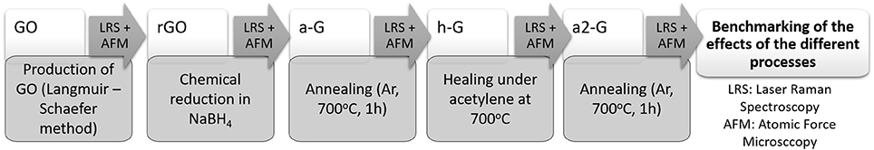
Figure 1. The process flow chart of the current study.
Morphological and Structural Evaluation via SEM, AFM, and Raman Spectroscopy
The morphology of the GO and the surface coverage of the Si substrate with GO flakes were studied via SEM using the JEOL JSM 6510 LV SEM/Oxford Instruments. Additionally, Atomic Force Microscopy (AFM) images were recorded in tapping mode with a Bruker Multimode 3D Nanoscope, using a silicon microfabricated cantilever type TAP-300G, with a tip radius <10 nm and a force constant range of ~20–75 N m−1.
The topography and quality of GO, rGO, a-G, h-G, and a2-G were studied after each process. The Si substrates used for this study had marked coordinates printed on their surface by lithography so as to facilitate the study of the same area in each step. All the spectra were recorded under the same experimental conditions, using the Labram HR system by HORIBA Scientific. Two spectral regions were evaluated for each case, namely the first order (1,050–1,750 cm−1) and the second order (2,400–3,100 cm−1). The 514.5 green line of an air cooled Ar-Ion Laser was employed for the Raman excitation using a confocal aperture of 150. The resulting spot with the × 100 objective was of submicron dimensions and the laser power at the focal plane was ca. 1.5 mW. An of 20 × 20 μm2 to 30 × 30 μm2 area was scanned after each applied process using a 2 μm step. The monitored area was defined in relation the center of four preselected markers with an accuracy of 2 μm for both Raman and AFM measurements.
Lorentzian and Gaussian distributions were used for spectral deconvolution along with an endpoint weighted linear baseline. The fitting procedure facilitated the quantification of the characteristics of each vibrational mode, i.e., Position, Intensity and Full Width at Half Maximum (FWHM).
Results and Discussion
The ODA-GO flakes distribution and the surface coverage of the Si substrate were initially examined via SEM and a representative micrograph is presented in Figure 2. The image confirmed the extensive surface coverage of the substrate with single graphene flakes of various sizes. Additionally, the optical micrographs presented in Figure 3, depict the evolution of the ODA-GO flakes through the various processing steps to r-GO, to a-G, to h-G, and then to a2-G. Optical microscopy was reported to be able to distinguish between GO and rGO since the reflection to incident light is improved by efficient reduction (Pei and Cheng, 2011). As can be seen, the reduction process of the GO sample in NaBH4 did not effectively altered the reflectivity of the sample, Figure 3b. On the other hand, the thermal annealing led to increased reflectivity (Figure 3C). Moreover, the optical micrographs of the proposed healing step and second annealing step (Figures 3D,E respectively) exhibited reduced surface reflectivity, which was the first implications that the samples have been covered with unwanted carbon byproducts.
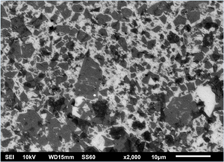
Figure 2. SEM micrograph of the GO flakes onto the Si substrate.
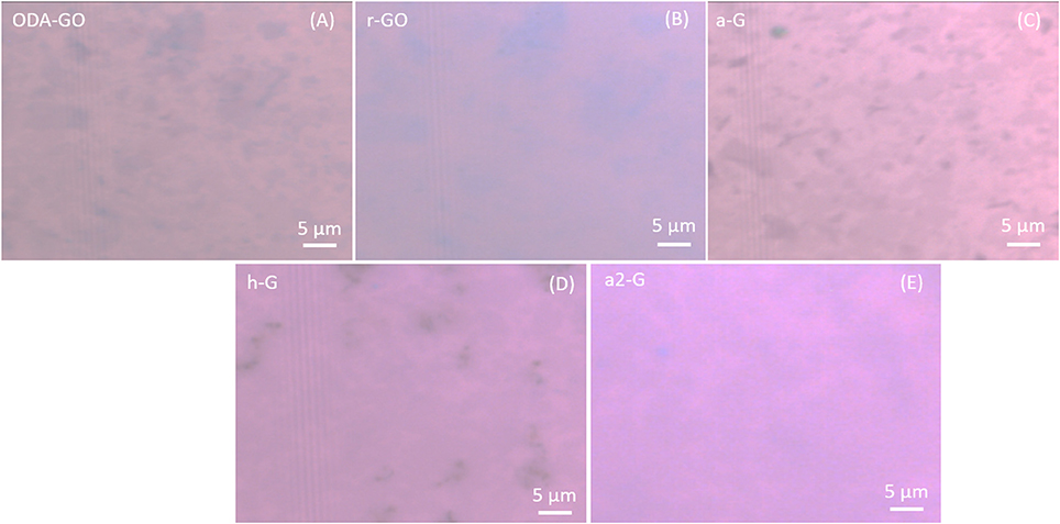
Figure 3. Optical micrographs of the samples after each different process. (A) As deposited ODA-GO, (B) r-GO, (C) a-G, (D) h-G, and (E) a2-G.
A direct comparison of the vibrational response of the samples after each process revealed substantial differences in their structures. Characteristic Raman spectra of the GO, rGO, a-G, h-G, and a2-G after each processing step are depicted in Figure 4. The spectrum of the graphite material used for the production of the GO is also included for comparison. The fitting procedure used for the calculation of the characteristics of the vibrational modes in each case is also presented in Figure 4 and these modes are annotated in the plot. The initial graphite material exhibited the two well-known graphitic vibrational modes. The G or graphitic band, positioned at 1,575 cm−1 and the 2D band, positioned at 2,716 cm−1. The former band corresponds to the in plane bond stretching of pairs of C atoms with sp2 hybridization and the latter one is the overtone of the D peak and represents a double resonance process (Ferrari, 2007).
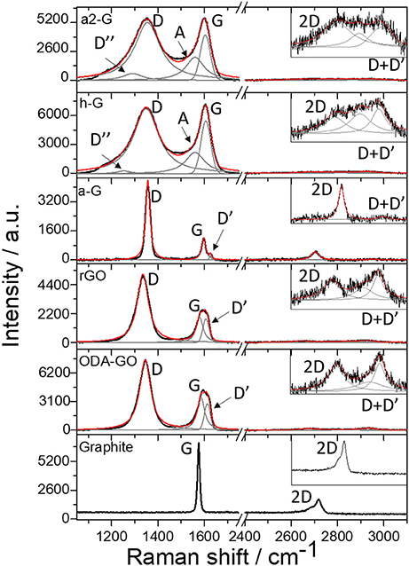
Figure 4. Raman spectra of the studied samples. The black lines represent the raw spectra, the gray lines correspond to the individual distributions used for the fitting procedure and the red line is the cumulative fitting curve. Notations for all the encountered vibrational modes can also be seen.
The rest of the samples presented two additional disorder induced vibrational modes. The D mode located at 1,330–1,350 which is an intervalley process, originating from the transverse optical phonons around the Brillouin zone boundary K (Martins Ferreira et al., 2010). The D + D' mode located at ~2,900 cm−1, which is a combination band of the D and the D' vibrations. Additionally, the ODA-GO, the rGO and the a-G samples presented the D' vibrational mode located at ~1,620 cm−1. This band appeared as a shoulder of the G band and together with the D band is associated to lattice defects (Ferrari and Basko, 2013). The D' band was not traceable for h-G and a2-G possibly due to the bandwidth of the involved convoluted peaks in the vicinity of the anticipated position. Furthermore, the h-G and a2-G samples presented two additional vibrations corresponding to the presence of amorphous carbon or pyro carbons (Merlen et al., 2017).
Further discussion on the effects of each procedure on the morphology and structure of the samples will be presented in the following sections. The features of interest for the Raman study were (i) the Position of the G vibrational mode—the displacement of the Raman bands to lower (higher) wavenumbers is called a redshift (blueshift) and is observed when the lattice of a crystalline material is under tension (compression), (ii) the ID/IG ratio which indicates the amount of the present defects with respect to the graphitic ordering of the structure, (iii) the I2D/IG ratio which is close to 2 for defect free graphene (Wall, 2011), and (iv) the FWHM of all the vibrational modes, which corresponds to the size distribution of the features causing the presence of each band.
ODA-GO flakes with well-defined edges were observed in the AFM micrographs (Figure 5A), verifying the formation of a hybrid Langmuir film at the air-dispersion interface and the subsequent deposition of the hybrid graphene oxide sheets (ODA-GO) on the hydrophobic Si-wafer surface. When the Langmuir film was compressed at a surface pressure of 20 mN m−1, the ODA-GO platelets contacted each other, leaving only small voids between them. The flake size distribution (Figure 5A left) revealed a high surface coverage which led to a continuous, close-packed array with a relatively low amount of cracks and wrinkles. The average thickness of the flakes was 1.5–2 nm as derived from the topographical height profile (Figure 5B) which corresponds to the black line in the higher magnification image (Figure 5A right). This value is larger than the value of 0.61 nm predicted for a single graphene oxide layer (Dékány et al., 1998) and is attributed to the ODA layer positioned underneath the GO sheet. Even without the presence of ODA molecules, the height of single GO layers was reported to be in the range of 1.1 ± 0.2 nm due to the existence of absorbed water molecules (Schniepp et al., 2006; Gómez-Navarro et al., 2007).
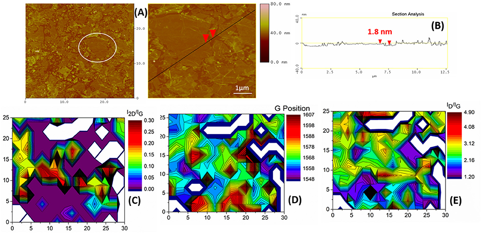
Figure 5. ODA-GO flakes deposited onto the Si substrate. (A) A low magnification AFM image (left) of the flake size distribution. The white circle highlights the area of the high magnification image (right). The black line and the red arrows indicate the section and point of measurement, respectively for (B), which is a section analysis with an indicative height measurement. (C) Raman 2D contour plot of the I2D/IG. (D) Raman 2D contour plot of the G position. (E) Raman 2D contour plot of the ID/IG ratio. Axis dimensions in all Raman plots are in μm.
The characteristic Raman spectra of the ODA-GO flakes (Figure 4) suggested that a significant amount of defects were present in the structure. The presence of the D and the D' vibrational modes, as well as the low intensity D+D' combination band were indicative of high defect density. The amount of defects in the form of heteroatoms, vacancies, line defects and edges was quantified by the large FWHM values of the D peak (Table 1) and plotted as the ID/IG ratio in a 2D contour plot (Figure 5E). Most of the surface of the ODA-GO sample presented ID/IG values in the range of 1.2–2.7, but a few highly defective points were also present on the surface of the Si wafer corresponding to values of up to 4.9. A comparison of this ratio plot with the 2D contour plot (Figure 5C) with the G band position (Figure 5D) revealed that areas with ID/IG values lower than 2 also presented higher G position, closer to 1,600 cm−1, but very low I2D/IG ratio mainly due to the small intensity of the 2D band. In comparison to the graphite spectrum, the G band of ODA-GO presented both redshift and blueshift in different areas (Table 1).
Table 1. Characteristics of the Raman Vibrational modes as evaluated by the fitting procedure.
Overall, the AFM showed that ODA-GO flakes with 1.5–2 nm average height and distinct ripples and cracks on their surface were deposited onto the Si substrate. The Raman spectrum was typical of GO with high defect density. In comparison to the initial graphite, the ODA-GO demonstrated both tensile and compressive strains mainly due to the presence of the surfactant molecules and the oxygen atoms in the GO lattice.
The next process included the reduction of the ODA-GO in a chemical agent in order to remove the surfactant molecules and eliminate the oxygen moieties from the ODA-GO surface. Figure 6 presents the AFM image of rGO sheets, which had a thickness of 1.9 nm. The reduction in the ODA-GO film influenced the morphology of the flakes due to the incorporation of stresses in the rGO lattice. The stresses were caused by the removal of the oxygen moieties. After reduction, the wrinkles of the GO sheets could still be distinguished. The bright spots corresponded to the remaining NaBH4 that was not totally removed by washing the sample after the reduction process. The formation of such ripples has also been reported in literature but for annealed graphene samples and has been attributed to stress effects caused by the annealing treatment (Xie et al., 2014), or to strain induced conformation of the graphene layers in annealed few layer graphene (Alyobi et al., 2017). These ripples are an intrinsic feature of graphene and have been reported to affect its electronic properties. Thus, the control of their formation and structure has also been a subject of study (Bao et al., 2009).
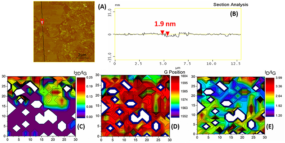
Figure 6. r-GO flakes onto the Si substrate. (A) A high magnification AFM image. The black line and the red arrows indicate the section and point of measurement, respectively for (B), which is a section analysis with an indicative height measurement. (C) Raman 2D contour plot of the I2D/IG. (D) Raman 2D contour plot of the G position. (E) Raman 2D contour plot of the ID/IG ratio. Axis dimensions in all Raman plots are in μm.
The vibrational response of r-GO did not seem to be significantly altered in comparison to the ODA-GO (Figure 4). However, a closer examination of the peak properties showed that some defects were eliminated. This was indicated by (i) the reduction in the FWHM values of the D mode by ca. 6 cm−1 (Table 1) and (ii) the reduced ID/IG ratio (Figure 6E). rGO exhibited ID/IG values in the range of 1.2–1.9 along most of its surface, and the few highly defective points corresponded to values of up to 3.98. The G band position (Figure 6D) suggested areas with a variety of crystallinity, closely resembling the differences in height shown in the AFM Figure 6A. The position of the G band was also considerably increased by almost 16 cm−1 (Table 1) indicating an increase in the crystalline ordering of the rGO lattice due to the reduction process and confirming the transition from graphite toward nanocrystalline graphene (Ferrari and Basko, 2013). On the other hand, the I2D/IG ratio values (Figure 6C) were slightly reduced in comparison to ODA-GO.
Overall, the reduction process did not alter the morphology and thickness of the rGO as shown by AFM while it successfully eliminated some of the defects from the GO lattice as suggested by the Raman analysis.
Then, a thermal annealing step was conducted in order to further eliminate the oxygen groups from the rGO surface and to partially restore the graphene properties. The topography of the annealed surface revealed a significant reduction in the thickness of the defected graphene nanosheets, which exhibited an average thickness of 0.9 nm ± 0.3 nm (Figure 7B). Some folds were also clearly observed in the edges of the graphene flakes with thickness of 3.1 nm (Figure 7C). This step also caused some stress relief from the graphene lattice attributed to the removal of a great amount of oxygen which led to the formation of grain boundaries on the graphene flake (Figure 7A).
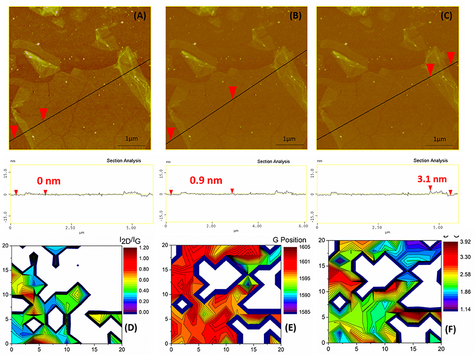
Figure 7. a-G flakes onto the Si substrate. (A–C) top: High magnification AFM image of a cross section, black line, with the red arrows indicating the point of measurement in each case. (A–C) bottom: The section analysis with the respective height measurements. (D) Raman 2D contour plot of the I2D/IG. (E) Raman 2D contour plot of the G position. (F) Raman 2D contour plot of the ID/IG ratio. Axis dimensions in all Raman plots are in μm.
The vibrational characteristics of rGO were also significantly affected by thermal annealing, as can be seen in Figure 4. The characteristic Raman spectra have been significantly altered to finally resemble that of a defected single layer graphene. The FWHM of the D mode reduced by 31 cm−1 to half of its previous value suggesting considerably reduced defect size distribution and the position of the D mode increased by 10 cm−1. In addition, all defect induced modes were greatly modified; the D' peak shrank to a small shoulder, shifted by 10 cm−1 to higher vibrational frequencies, and the combination band D+D' almost disappeared in the spectral noise. Moreover, the 2D vibrational mode of a single graphene layer appeared at 2,700 cm−1 with an average FWHM of 43 cm−1 (Table 1). Regarding the G peak position, the a-G sample presented average values of almost 1,600 cm−1 and a high homogeneity in the peak positions along the Si surface (Figure 7E). A G band position close to 1,600 cm−1 can be attributed to a nanocrystalline material (Ferrari, 2007). Additionally, the ID/IG ratio (Figure 7F), presented similar values to the rGO, possibly due to the grain boundaries, shown in the AFM images of Figure 7, which enhance defect induced Raman vibrations. This argument is further strengthened by the fact that the FWHM of the D peak was reduced to ~ 30 cm−1 meaning that there existed less defects types producing defect induced Raman vibrations. On the other hand, the I2D/IG showed greatly enhanced values as can be seen in Figure 7D, reaching up to 1.2.
Summarizing, the annealing process eliminated most of the defects except from the lattice defects (edges, line defects and vacancies) as indicated by the Raman study. The successful conversion of rGO to single layer nanocrystalline graphene (a-G) was confirmed by both Raman and AFM measurements which indicated a thickness of 0.9 nm.
Although single layer graphene was recovered from the ODA-GO as was confirmed by AFM and Raman measurements, the presence of defect-induced bands indicated that not all defects were eliminated. With a view to restore the graphene lattice, a healing step was performed which has previously been reported in literature to positively affect the ordering of the crystal lattice and increase graphene's electrical properties (Sundaram et al., 2009). The effects of the healing process were not the anticipated ones. The thickness of the graphene sheets did not change as expected and was estimated to be 0.9 nm, as can be seen in Figures 8A,B but the graphene flakes are not clearly observed anymore. This might be attributed to the creation of a thin veil of carbon on the entire surface of the h-G.
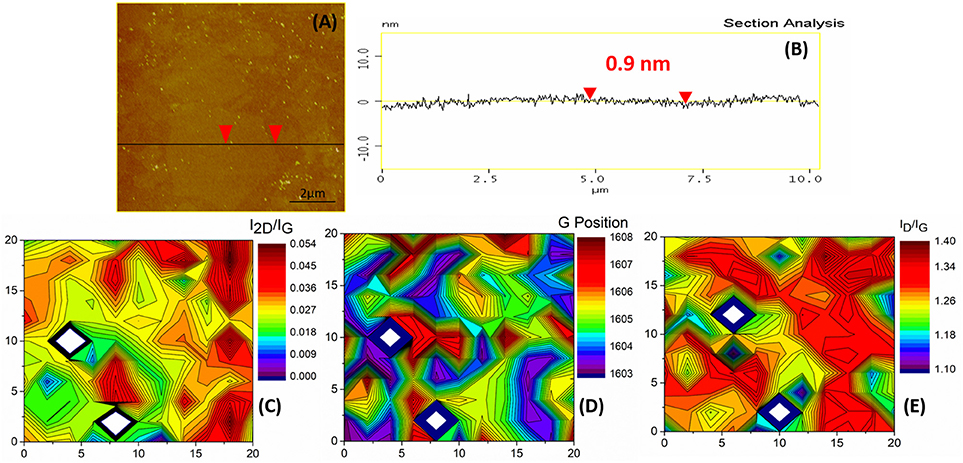
Figure 8. h-G flakes onto the Si substrate. (A) A high magnification AFM image. The black line and the red arrows indicate the section and point of measurement, respectively for (B), which is a section analysis with an indicative height measurement. (C) Raman 2D contour plot of the I2D/IG. (D) Raman 2D contour plot of the G position. (E) Raman 2D contour plot of the ID/IG ratio. Axis dimensions in all Raman plots are in μm.
The Raman spectrum of h-G was also altered considerably as can be seen in Figure 4. The FWHM of all peaks increased (Table 1) and both the D” and A vibrational modes appeared. These are attributed to amorphous carbon (Merlen et al., 2017). The D' band was considered together with the G band as a single mode shifted to 1,600 cm−1 confirming the presence of nanocrystalline graphite as proposed by Ferrari and Basko (Ferrari and Basko, 2013). The 2D and D+D' bands were also greatly suppressed and altered in shape. The position of the D vibrational mode was shifted to even higher wavenumbers and the distribution of the position was narrower than before (Figure 8D). Additionally, the I2D/IG ratio was suppressed to values below 0.1 (Figure 8C), due to the fact that the 2D band was barely visible. On the other hand, the ID/IG ratio was enhanced in comparison to the previous processing steps, presenting values in the range of 1.09–1.38 and increased homogeneity on all the studied surface (Figure 8E). The homogeneous distribution of all Raman features after the healing process, along with the appearance of the D” and the A bands were in full agreement with the AFM observations which also indicated that a thin veil of nanocrystalline carbon hindered the study of the underlying single layer graphene flakes (SLGF).
In short, the healing process did not alter the morphology and thickness of the graphene flake as shown by AFM while it resulted in the formation of a thin graphite veil on the surface of the graphene flakes. This veil was a mixture of mainly nanocrystalline carbon with a small amount of amorphous carbon.
In an attempt to eliminate the carbon byproducts, an additional annealing step identical to the first thermal annealing was performed. The AFM images acquired after that step (Figure 9A) remained blurred and that was a first indication that at least part of the carbon veil was still present on the graphene surface. The thickness of graphene sheets was equal to the value of 1 nm, as can be seen in Figure 9B. The same results were also acquired via Raman spectroscopy (Figure 4). The wide D peak still existed, although with slightly decreased FWHM by 7 cm−1. The D” and A bands attributed to amorphous carbon were not eliminated and the D' band was again considered together with the G band as a single distribution. Regarding the second order Raman features, the 2D band remained barely visible and broad, overlapping with the other second order vibrations. These results are also reflected in the 2D contour maps of the I2D/IG ratio, (Figure 9C) and the G band position (Figure 9D). On the other hand, the ID/IG ratio was further enhanced in comparison to the previous processing steps, presenting values in the range of 0.97–1.28 (Figure 9E). The Raman results were again in agreement with the AFM measurements indicating that a part of the thin carbon veil was not successfully removed and that hindered the study of the underlying SLGF.
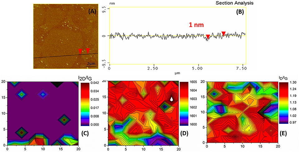
Figure 9. a2-G flakes onto the Si substrate. (A) A high magnification AFM image. The black line and the red arrows indicate the section and point of measurement, respectively for (B), which is a section analysis with an indicative height measurement. (C) Raman 2D contour plot of the I2D/IG. (D) Raman 2D contour plot of the G position. (E) Raman 2D contour plot of the ID/IG ratio. Axis dimensions in all Raman plots are in μm.
Overall, the second annealing step did not alter the morphology and height of the h-G, in contrast to the first annealing step which effectively reduced the thickness of the a-G, as indicated by the AFM. The thin veil of mainly nanocrystalline carbon which was produced on the surface of the h-G during the healing process was not eliminated by the annealing step as shown by Raman measurements.
Conclusions
This study involved the preparation of GO flakes deposited on Si wafer by the Langmuir-Blodgett method, and its subsequent reduction, annealing, healing, and second annealing. SLGF were recovered by the reduction and thermal annealing of the GO flakes. The height distributions obtained AFM images confirmed that a-G was single layer. The topography and the structure of the produced SLGF was also evaluated via Raman mapping. To our knowledge, this is the first systematic study regarding the effects of the reduction and thermal annealing of SLGF produced via the Langmuir-Blodgett method. The spectral characteristics of both the first and the second order vibrational modes were employed to highlight the process induced changes in the recovery of SLGF produced from GO.
The initial defects present in ODA-GO were initially reduced after the reduction process and substantially reduced after annealing, as was indicated by the characteristic disorder induced Raman vibrational modes. Although the reduction process did not affect the layer thickness, annealing resulted to a 0.9 nm thickness which is characteristic of single layer graphene. Both the reduction and annealing processes resulted to higher wavenumber positions, particularly for the G and the 2D lines, indicating the formation of nanocrystalline graphene via the stress relief from the removal of functional groups and heteroatoms. The Raman spectrum of a-G indicated the substantial reduction of all defects except from some lattice defects line defects, vacancies and edges, as was indicated by the reduction of the FWHM of the disorder induced vibrational modes.
To further eliminate the lattice defects a healing process was applied. However, the healing step did not result to defect elimination; albeit, it led to the deposition of a thin veil of nanocrystalline and amorphous carbon on the whole surface of the Si wafer, as was indicated by the merging of the G and D' lines and the emergence of the D” and A vibrational modes in the first order spectrum, respectively. Further annealing was not found to substantially the deposited nanocrystalline and amorphous carbon.
Author Contributions
KT was the main author and performed the spectral fitting. AK performed the Raman measurements. NC manufactured the Go flakes. DG overviewed the manufacturing. AP overviewed the Raman study and the manuscript writing.
Conflict of Interest Statement
The authors declare that the research was conducted in the absence of any commercial or financial relationships that could be construed as a potential conflict of interest.
References
Ajlani, H., Othmen, R., Cavanna, A., Madouri, A., and Oueslati, M. (2016). Raman spectroscopy study of annealed incommensurate graphene bilayer on SiO2substrate. Superlat. Microstruct. 90, 96–106. doi: 10.1016/j.spmi.2015.12.009
Alyobi, M., Barnett, C., and Cobley, R. (2017). Effects of thermal annealing on the properties of mechanically exfoliated suspended and on-substrate few-layer graphene. Crystals 7:349. doi: 10.3390/cryst7110349
Aoki, H., and Dresselhaus, M. S. (eds.). (2014). Physics of Graphene. Cham; Heidelberg; New York, NY; Dordrecht; London: Springer International Publishing.
Avouris, P., and Dimitrakopoulos, C. (2012). Graphene: synthesis and applications. Mater. Today 15, 86–97. doi: 10.1016/S1369-7021(12)70044-5
Bao, W., Miao, F., Chen, Z., Zhang, H., Jang, W., Dames, C., et al. (2009). Controlled ripple texturing of suspended graphene and ultrathin graphite membranes. Nat. Nanotechnol. 4, 562–566. doi: 10.1038/nnano.2009.191
Bhuyan, M. S. A., Uddin, M. N., Islam, M. M., Bipasha, F. A., and Hossain, S. S. (2016). Synthesis of Graphene. Int. Nano Lett. 6, 65–83. doi: 10.1007/s40089-015-0176-1
Binder, R. (2017). Optical Properties of Graphene. New Jersey, NJ; London; Singapore; Beijing; Shanghai; Hong Kong; Taipei; Chennai; Tokyo: World Scientific Publishing Co. Pte. Ltd.
Bokobza, L., Bruneel, J. L., and Couzi, M. (2014). Raman spectroscopy as a tool for the analysis of carbon-based materials (highly oriented pyrolitic graphite, multilayer graphene and multiwall carbon nanotubes) and of some of their elastomeric composites. Vib. Spectrosc. 74, 57–63. doi: 10.1016/j.vibspec.2014.07.009
Bonaccorso, F., Lombardo, A., Hasan, T., Sun, Z., Colombo, L., and Ferrari, A. C. (2012). Production and processing of graphene and 2d crystals. Mater. Today 15, 564–589. doi: 10.1016/S1369-7021(13)70014-2
Botcha, V. D., Narayanam, P. K., Singh, G., Talwar, S. S., Srinivasa, R. S., and Major, S. S. (2014). Effect of substrate and subphase conditions on the surface morphology of graphene oxide sheets prepared by langmuir-blodgett technique. Colloids Surf. A Physicochem. Eng. Aspects 452, 65–72. doi: 10.1016/j.colsurfa.2014.03.077
Dékány, I., Krüger-Grasser, R., and Weiss, A. (1998). Selective liquid sorption properties of hydrophobized graphite oxide nanostructures. Colloid Polym. Sci. 276, 570–576. doi: 10.1007/s003960050283
Dresselhaus, M. S., Dresselhaus, G., and Hofmann, M. (2008). Raman spectroscopy as a probe of graphene and carbon nanotubes. Philos. Trans. R. Soc. A 366, 231–236. doi: 10.1098/rsta.2007.2155
Ferrari, A. C., and Basko, D. M. (2013). Raman spectroscopy as a versatile tool for studying the properties of graphene. Nat. Nanotechnol. 8, 235–246. doi: 10.1038/nnano.2013.46
Ferrari, A. C. (2007). Raman spectroscopy of graphene and graphite : disorder, electron – phonon coupling, doping and nonadiabatic effects. Solid State Commun. 143, 47–57. doi: 10.1016/j.ssc.2007.03.052
Geim, A. K., and Novoselov, K. S. (2007). Graphene to rise_Nature_2007. Nat. Mater. 6, 183–191. doi: 10.1038/nmat1849
Gengler, R. (2010). An Introduction to the Hybrid Langmuir-Schaefer Approach. Groningen: University of Groningen. Available online at: https://www.rug.nl/research/portal/publications/a-modified-langmuir-schaefer-method-for-the-creation-of-functional-thin-films(8d102806-1950-4ee8-a84a-79b7f29312f2)/export.html
Gómez-Navarro, C., Thomas Weitz, R., Bittner, A. M., Scolari, M., Mews, A., Burghard, M., et al. (2007). Electronic transport properties of individual chemically reduced graphene oxide sheets. Nano Lett. 7, 3499–3503. doi: 10.1021/nl072090c
Intellectual Property Office GOV.UK (2015). Graphene: The Worldwide Patent Landscape in 2015. Intellectual Property Office (GOV.UK), 30. Available online at: https://www.gov.uk/government/organisations/intellectual-property-office
Lin, Y. C., Lu, C. C., Yeh, C. H., Jin, C., Suenaga, K., and Chiu, P. W. (2012). Graphene annealing: how clean can it be? Nano Lett. 12, 414–419. doi: 10.1021/nl203733r
Martins Ferreira, E. H., Moutinho, M. V. O., Stavale, F., Lucchese, M. M., Capaz, R. B., Achete, C. A., et al. (2010). Evolution of the raman spectra from single-, few-, and many-layer graphene with increasing disorder. Phys. Rev. B 82:125429. doi: 10.1103/PhysRevB.82.125429
Merlen, A., Buijnsters, J., and Pardanaud, C. (2017). A guide to and review of the use of multiwavelength raman spectroscopy for characterizing defective aromatic carbon solids: from graphene to amorphous carbons. Coatings. 7:153. doi: 10.3390/coatings7100153
Papageorgiou, D. G., Kinloch, I. A., and Young, R. J. (2017). Mechanical properties of graphene and graphene-based nanocomposites. Prog. Mater. Sci. 90, 75–127. doi: 10.1016/j.pmatsci.2017.07.004
Pei, S., and Cheng, H.-M. (2011). The reduction of graphene oxide. Carbon N.Y. 50, 3210–3228. doi: 10.1016/j.carbon.2011.11.010
Pop, E., Varshney, V., and Roy, A. K. (2012). Thermal properties of graphene: fundamentals and applications. MRS Bull. 37, 1273–1281. doi: 10.1557/mrs.2012.203
Schniepp, H. C., Li, J. L., McAllister, M. J., Sai, H., Herrera-Alonson, M., Adamson, D. H., et al. (2006). Functionalized single graphene sheets derived from splitting graphite oxide. J. Phys. Chem. B 110, 8535–8539. doi: 10.1021/jp060936f
Sundaram, R. S., Go, C., Olea, D., Kern, K., Burghard, M., and Go, J. (2009). Chemical vapor deposition repair of graphene oxide : a route to highly conductive graphene Monolayers. Adv. Mater. 46, 83–86. doi: 10.1002/adma.200901582
Wall, M. (2011). The Raman Spectroscopy of Graphene and the Determination of Layer Thickness. Application Note: 52252, Madison, WI: Thermo Fisher Scientific.
Xie, W. G., Lai, X., Wang, X. M., Wan, X., Yan, M. L., Mai, W. J., et al. (2014). Influence of annealing on raman spectrum of graphene in different gaseous environments. Spectr. Lett. 47, 465–470. doi: 10.1080/00387010.2013.809595
Xueshen, W., Jinjin, L., and Qing, Z. (2013). Thermal annealing of exfoliated graphene. J. Nanomat. 8, 1–6. doi: 10.1155/2013/101765
Keywords: graphene oxide, single graphene flakes, 2D Raman mapping, AFM, annealing, healing, reduction
Citation: Tsirka K, Katsiki A, Chalmpes N, Gournis D and Paipetis AS (2018) Mapping of Graphene Oxide and Single Layer Graphene Flakes—Defects Annealing and Healing. Front. Mater. 5:37. doi: 10.3389/fmats.2018.00037
Received: 30 January 2018; Accepted: 29 May 2018;
Published: 14 June 2018.
Edited by:
Guohai Chen, National Institute of Advanced Industrial Science and Technology (AIST), JapanReviewed by:
Ji Chen, University of Maryland, College Park, United StatesYenan Song, East China Normal University, China
Rajyashree Sundaram, Japan Society for the Promotion of Science (JSPS), Japan
Copyright © 2018 Tsirka, Katsiki, Chalmpes, Gournis and Paipetis. This is an open-access article distributed under the terms of the Creative Commons Attribution License (CC BY). The use, distribution or reproduction in other forums is permitted, provided the original author(s) and the copyright owner are credited and that the original publication in this journal is cited, in accordance with accepted academic practice. No use, distribution or reproduction is permitted which does not comply with these terms.
*Correspondence: Alkiviadis S. Paipetis, cGFpcGV0aXNAY2MudW9pLmdy