 Zenggui Wang1,2
 Xi Yang2*Zhenhai Yang2Wei Guo2Liujin Lin2Nan Li2Ershuai Jiang2Jianfeng Zhang1*Baojie Yan2Jichun Ye2*
- 1Faculty of Material Science and Chemical Engineering, Ningbo University, Ningbo, China
- 2Ningbo Institute of Material Technology and Engineering, Chinese Academy of Sciences, Ningbo, China
In recent years, ultrathin Ag films (UTAFs), which are attractive owing to its extremely low resistance, relatively high transparency, excellent mechanical flexibility, and mature mass production, have been reported as potential candidates to replace traditional indium tin oxide (ITO). To achieve a high-quality UTAF, a nucleation-inducing seed layer (NISL) is required to address the issue of irregular Ag islands growth. However, the structures of films so deposited are still far from being ideal and consist of rough surfaces with high densities of voids and grain boundaries when the film thickness is < ~6 nm. Here, a hybrid structure composed of a gold (Au)/polyethyleneimine (PEI) bilayer is employed as a high-density NISL for the fabrication of an UTAF. Compared to the conventional single-layered PEI NISL that physisorbed on the substrate via the weak electrostatic attraction between the negatively charged substrate and the positively charged amine groups in PEI, our novel bilayered Au/PEI NISL exhibits a much higher density of nucleation sites due to the formation of strong coordinate covalent bonds between the Au atoms and amine groups. As a result, the percolation threshold thickness of the UTAF based on the Au/PEI bilayer can be reduced to as low as 3 nm. After capping with a high-refractive-index tantalum pentoxide (Ta2O5) anti-reflection layer, the resultant Au/PEI/8 nm Ag/30 nm Ta2O5 (APAT) electrode exhibits an excellent optoelectrical performance with a sheet resistance of 9.07 Ω/sq and transmittance of 92.9% in the spectral range of 400–800 nm as well as outstanding long-term environmental and mechanical stabilities. The findings demonstrate a novel strategy for the development of high-performance UTAF-based transparent electrodes.
Introduction
The rapid growth of optoelectronic devices including flexible displays, touchscreens, electrochromics, light-emitting diodes, and photovoltaic cells requires the development of flexible transparent conductive electrodes (FTCEs) possessing high optical transparency, low sheet resistance, good mechanical flexibility, and superior environmental stability (Hecht et al., 2011; Morales-Masis et al., 2017). Traditional transparent conductive oxide, typically represented by indium tin oxide (ITO), is the most widely used TCE owing to its excellent electrical conductivity and light transmittance; however, the high-temperature fabrication, its brittle nature under repeated bending condition, opacity in the near-infrared region, and high raw material cost hinder its application in flexible and large-area devices (Ellmer, 2012). Therefore, various candidate materials based on carbon nanotubes, graphene, conducting polymers, metallic nanowires, metal meshes, or their hybrids have been extensively investigated to replace ITO as novel FTCEs (Zhang et al., 2005; Nair et al., 2008; Guo et al., 2013; Hsu et al., 2013; Ricciardulli et al., 2018). Although all the above-mentioned ITO alternatives have experienced a rapid development and achieved different levels of success in commercial applications, some of them still suffer from one or more drawbacks such as poor stability, less adhesion, large surface roughness, high fabrication cost, and strong optical scattering, and do not always achieve a competitive trade-off between optical transmittance (T) and electrical sheet resistance (Rsheet) (Yun, 2017).
Recently, FTCEs based on ultrathin metal films (UTMFs) with thickness below 10 nm have generated great interest owing to their high electrical conductivity, good mechanical stability, low surface roughness, and mature fabrication technology (Hatton et al., 2003; Illhwan and Jong-Lam, 2015; Maniyara et al., 2016). However, the metal film with such a low film thickness deposited on a foreign substrate tends to disorderly migrate and aggregate as irregular islands (Volmer-Weber growth mode) due to the surface energy mismatch with the substrate, and consequently exhibits a discrete granular morphology with a high electrical resistivity as well as an additional light absorption and scattering loss, which severely affect both the Rsheet and T of the resulting TCE (Zhang et al., 2014). To address this morphological deficiency, an ultrathin nucleation-inducing seed layer (NISL) composed of high-surface energy metals, transition metal oxides, organics with thiol and amine functional groups, or a hybrid thereof is usually placed underneath the evaporated metal film to suppress the growth of isolated islands and promote the formation of a highly continuous UTMF (Zhang et al., 1997; Meiss et al., 2008; Logeeswaran et al., 2009; Liu et al., 2010; Stec et al., 2011; Salinas et al., 2012; Hutter et al., 2013; Jeong and Kim, 2013; Schubert et al., 2013, 2014; Kim et al., 2014; Luo et al., 2014; Wang et al., 2014; Zou et al., 2014; Hutter and Hatton, 2015; Chang et al., 2016; Xue et al., 2016; Ghosh and Leo, 2017; Yang et al., 2017; Zheng et al., 2017; Zhu et al., 2018). Among them, a solution-processed cationic polyelectrolyte of amine-terminated polyethyleneimine (PEI), which can be easily physisorbed onto various substrates based on the electrostatic attraction between opposite charges, has been proved a commendable NISL for achieving high-quality and large-area ultrathin Ag films (UTAFs) owing to its low-cost, low-temperature and high-throughput fabrication compared with other physical vapor- deposited and chemisorbed films (Min et al., 2014; Kang et al., 2015). Although an effective reduction in the percolation threshold thickness of Ag can be achieved by employing the PEI NISL, the thickness of the Ag films actually applied in TCEs is still above 6 nm and these Ag films possess a narrow transmittance spectrum, decreasing from ~75% peak transmittance at 400 nm to below 60% at 800 nm. This is because the structures of Ag films so deposited are still far from being ideal and consist of rough surfaces with high densities of voids and grain boundaries when the film thickness is < 6 nm. Recently, it was demonstrated that the density of the sites that are chemically reactive with the evaporated Ag atoms could be determined by the concentration of functional amine groups on the NISL surface (Jeong et al., 2017). However, the adsorbed amine groups in the PEI NISL is always limited by the poor electrostatic attraction to the weakly charged substrate as well as the strong repulsion between the PEI chain entanglements (Hoogeveen et al., 1996; Li et al., 1997; Dobrynin et al., 2000). Therefore, to achieve a high-performance UTAF with a lower thickness while maintaining a smooth surface, it is very essential to develop a novel method to improve the density of amine groups in the adsorbed PEI NISL.
In this work, a novel bilayered structure of Au/PEI is employed as a high-density NISL to obtain a high-performance UTAF. The bottom Au layer is introduced to improve the adsorption of PEI, while the top PEI layer is used to immobilize the incoming Ag atoms. Compared to the conventional single-layered PEI NISL that physisorbed on the substrate via the weak electrostatic attraction between the negatively charged substrate and the positively charged amine groups in PEI, our novel bilayered Au/PEI NISL exhibits a much higher density of nucleation sites due to the formation of strong coordinate covalent bonds between the Au atoms and amine groups; this is beneficial for the fabrication of UTAFs with high conductivities, low optical absorption losses, and smooth surfaces. As a result, the percolation threshold thickness of the UTAF based on the Au/PEI bilayer can be reduced to as low as 3 nm. After capping with a high-refractive-index tantalum pentoxide (Ta2O5) anti-reflection layer, the resultant Au/PEI/Ag/Ta2O5 (APAT) electrode exhibits an excellent optoelectrical performance with a Rsheet of 9.07 Ω/sq and T of 92.9% at a wavelength of 550 nm as well as outstanding long-term environmental and mechanical stabilities. This study demonstrates a novel strategy for the development of high-performance UTAF-based FTCEs.
Experiments
Electrode Fabrication
The quartz and PET substrates were cleaned with acetone, alcohol, and DI water, respectively, and then treated with ultraviolet-ozone. PEI (Sigma-Aldrich, linear type, 50 wt% in H2O) was diluted in DI water to prepare a 0.3 wt% aqueous solution. The samples were loaded into an electron beam chamber (Xinnan-Tech ZZS-500) (base pressure of 6 × 10⁻⁴ Pa) and a 6-Å-thick Au layer was deposited at a rate of 0.5 Å/s. A PEI film was then coated onto the substrates by immersing into the PEI solution for 10 min, rinsing with water, and drying under filtered a N2 flow. Finally, the samples were loaded into the electron beam chamber (base pressure of 6 × 10⁻⁴ Pa) to successively deposit Ag and Ta2O5 layers at a rate of 1.7 and 0.5 Å/s, respectively.
Characterization
The electrical properties of the films were measured using a four-point probe system (NAPSON CRESBOX). Typically, measurements were performed at 25 different positions on each film, and the average values of Rsheet were calculated. The transmittance in the spectral range of 400–800 nm was measured using a Perkin-Elmer Lambda 950 UV/Vis/NIR spectrophotometer equipped with a 150-mm-diameter integrating sphere including the substrates. Scanning electron microscopy (SEM) and the tapping-mode atomic force microscopic (AFM) measurements were conducted using a Hitachi S-4800 SEM and a Veeco 3100 SPM, respectively. ImageJ software was used to analyze the surface coverage of the Ag films. Optical calculations were implemented using the finite element method. The deposition rate and film thickness of the deposited materials were monitored by a quartz crystal oscillator mounted adjacent to the substrates. X-ray photoelectron spectroscopy (XPS) was performed onto the film deposited on single-side polished c-Si wafers using a Kratos AXIS Ultra delay-line detector system under ultrahigh vacuum with a monochromatic Al Kα X-ray source and a hemispherical analyzer.
Results and Discussion
Figure 1A illustrates the schematic diagrams of the Ag films initially grown on the bare substrate, conventional single-layered PEI, and novel bilayered Au/PEI NISLs. When the Ag film is deposited on the bare substrate, the Ag atoms coalesce with each other due to the strong cohesive force between the adatoms, resulting in rough 3D Ag islands. In the case of single-layered PEI, the amine groups in the PEI act as nucleation centers to suppress the growth of large metal islands during film deposition. Although the PEI polymer has the highest charge density currently available (23.3 mequiv./g in an aqueous solution when fully protonated), the actually deposited PEI monomers, which are physically absorbed onto the substrate through a weak electrostatic interaction between the positive protonated amine groups in the PEI monomers and the negatively charged OH groups on the substrate, are still limited by the poor surface charge density of most substrates as well as the repulsive intertrain interaction in PEI (Dobrynin et al., 2000; Gorin et al., 2009; Yu et al., 2013). However, for the novel bilayered Au/PEI NISL, the introduction of the Au subjacent layer can promote the adsorption of PEI and further immobilize the incoming evaporated Ag atoms. The driving force for the adsorption of PEI on the Au surface is the strong covalent interaction between the Au atoms and the amine groups in the PEI monomers. We expect that these strong covalent bonds can screen the repulsive interaction and firmly immobilize more PEI monomers, thus increasing the density of amine groups in the adsorbed PEI.
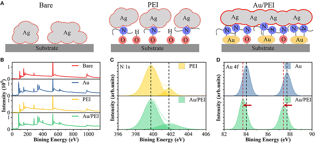
Figure 1. (A) Conceptual diagram of the growth mechanism of Ag film on bare substrate, conventional single-layered PEI, and novel bilayered Au/PEI NISLs. (B) XPS survey spectra of bare Si substrate before and after coating with Au, PEI, and Au/PEI NISLs. High-resolution normalized XPS spectra of (C) N1s and (D) Au 4f on different NISLs.
To validate the above-described assumption, we first compared the surface chemical composition of the adsorbed PEI with and without the 6-Å-thick Au precoated layer on the Si substrate by XPS. For comparison, Si substrates with and without the Au subjacent layer before PEI adsorption were used as reference samples. Figure 1B shows the survey spectra of these four samples. The atomic concentrations of various principal elements (C 1s, N 1s, Au 4f, and Si 2p) are listed in Table 1. The presence of N element in PEI and Au/PEI samples indicate the successful adsorption of PEI. The N atomic concentration in Au/PEI (9.67%) is higher than that in PEI (5.15%), suggesting an enhanced PEI adsorption in Au/PEI NISL. For clarity, fine XPS spectra of N 1s for PEI and Au/PEI were fitted by multiple Gaussians. As shown in Figure 1C, the deconvoluted N 1s region in the XPS spectra of both PEI and Au/PEI show two different components: the peak located at the low binding energy (BE) of 399.8 eV is attributed to the N element in the neutral amines, while that at the high BE of 401.8 eV is attributed to N+ in the protonated amines (Suriyanarayanan et al., 2013). It is noteworthy that the N 1s peak intensity in the Au/PEI spectrum at a high BE (with a [N+]/[N] ratio of 0.27) is ~1.7 times that of the single-layered PEI (with a [N+]/[N] ratio of 0.16), which suggests that the subjacent Au layer can significantly increase the number of protonated amines groups in the adsorbed PEI. To further indicate the interaction between Au and PEI during the adsorption of PEI on Au, the fine XPS spectra of Au 4f for Au and Au/PEI were measured and are shown in Figure 1D. Compared to bare Au, the Au 4f peaks of Au/PEI shifted toward a lower BE, with the Au 4f 7/2 and Au 4f 5/2 bands shifting from 84.0 and 87.7 eV to 83.7 and 87.4 eV, respectively. These chemical shifts indicate that the Au atoms accept the unshared electron pairs from the amines of the PEI layer to form coordinate covalent bonds (Wang et al., 2018). Therefore, more amine groups are protonated during the adsorption of PEI on Au, which is consistent with the XPS results of N 1s. Based on these results, we conclude that the adsorbed PEI monomers on the Au precoated layer are immobilized by a strong coordination reaction rather than the weak electrostatic interaction in the conventional adsorption of PEI without Au, thus resulting in a much higher density of PEI NISL.
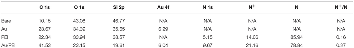
Table 1. Atomic concentration (%) of different samples determined by XPS analysis.
Further, we demonstrate the influence of high-density Au/PEI NISL on the nucleation of UTAF. Figures 2A–D show the SEM images of the surface morphologies of the 8-nm-thick Ag films on a bare glass and on different types of seed (Au, PEI, and Au/PEI) layers. The AFM images and the corresponding typical cross-section line profiles of the surfaces of Ag films are shown in Figures 2E-H. The Ag film directly deposited on a bare glass exhibits island-like structures with a large surface root-mean-square (RMS) roughness of 6.44 nm and a low surface coverage of 74.6%. The peak-to-valley ratio of the film is even higher than the film thickness, implying that the film is discontinuous over the microscopic dimension. In contrast, the Ag film with only the Au NISL shows a decrease in grain size with an RMS roughness of 2.09 nm. Although the Ag islands begin to connect, resulting in an improved surface coverage of 80.5%, a large number of voids still exist. The high surface coverage is possibly because the Au functions as a high-surface energy seed layer, and it is energetically more favorable for the Ag atoms to attach to the Au surface than to agglomerate together (Schubert et al., 2013). A similar but larger effect is noted for the Ag film grown on the PEI NISL, wherein more Ag islands are connected with each other with only a small number of voids on the surface, thus exhibiting a reduced RMS roughness of 1.52 nm and an increased surface coverage of 94.1%. The improvement in film continuity and uniformity is due to the immobilization of Ag atoms via strong coordination bond interactions to the amine groups on the PEI surface (Kang et al., 2015). However, when the Ag film is deposited on the Au/PEI hybrid NISL, the Ag film almost completely covers the entire substrate, exhibiting the lowest RMS roughness of 0.42 nm and the highest surface coverage of 98.4%. This excellent morphology of the Ag film on Au/PEI NISL can be ascribed to the high density of amine groups in Au/PEI, which act as a much higher-interface energy substrate with an a higher density of nucleation sites for the deposited Ag atoms.
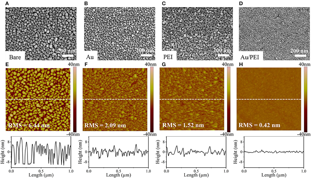
Figure 2. SEM and AFM images of 8-nm-thick Ag on top of (A,E) glass, (B,F) Au, (C,G) PEI, and (D,H) Au/PEI NISLs, respectively.
It is well-known that the abrupt change in morphology plays a vital role in both electrical and optical properties of a Ag film. The variation in Rsheet with thickness of the Ag thin films deposited on different substrates is shown in Figure 3A. In the case of bare substrate, the Rsheet of Ag film is infinite at a film thickness of < 12 nm, indicating the 3D growth of a discontinuous Ag film caused by the severe diffusion of Ag atoms on glass due to the stronger interaction between Ag atoms than that between Ag and glass. For thicknesses ≥ 12 nm, a dramatic drop in Rsheet by one order of magnitude can be observed, which suggests the coalescence of Ag islands at this percolation threshold thickness (Ghosh, 2012). For Ag films grown on Au, PEI, and Au/PEI NISLs, the same effects can be seen but at a lower percolation threshold thickness of 6, 4, and 3 nm, respectively, which are in good agreement with the changes in film morphology as mentioned above. Figure 3B shows the wavelength-dependent transmittance and corresponding Rsheet of 8-nm-thin Ag layers on varying substrates. It can be seen that the non-conductive bare Ag film is characterized by a valley at ~450 nm due to the excitation of strong localized surface plasmon resonance (SPR) induced by the isolated Ag islands (Xu et al., 2003). After the SPR peak, the transparency of the bare Ag gradually increased with wavelength, suggesting that the film is discontinuous and non-conductive. In contrast, by introducing the Au and PEI single-layered NISLs, the Rsheet of both the Ag films were reduced to 58.6 and 12.5 Ω/sq, respectively, which is indicative of the formation of percolation paths. In addition, the spectral shape of the transmittance curves changed and showed a weakened Ag SPR peak as well as a reduced T above 600 nm, evidencing the improved morphology of Ag films. The emergence of a new mild dip at ~ 520 nm in the transmittance of the Ag film on the Au single-layered NISL can be ascribed to the SPR induced by the Au (Daniel and Astruc, 2004). Strikingly, after employing the bilayered Au/PEI NISL, the Ag film delivers the lowest Rsheet of 9.07 Ω/sq, which is much lower than that of the conventional ITO (15–30 Ω/sq). The spectral shape of the transmittance curve remarkably changed to a flat profile over the entire wavelength range. Moreover, both the SPR peaks induced by Ag and Au are eliminated, indicating a smooth surface topography of a completely continuous Ag film without any parasitic absorption.
Figure 3. (A) Sheet resistance of Ag films on different NISLs as a function of Ag thickness. (B) Transmission spectra of 8-nm-thick Ag film on different NISLs. (C) Calculated transmittance of APAT film as a function of wavelength and thickness of Ta2O5 layers. (D) Transmittance spectra and (E) optical photographs of APAT films with various Ta2O5 thicknesses. The transmittance spectra of conventional ITO (black dashed line) is also shown for comparison.
Although the absorption loss of the Ag film can be counteracted by the introduction of NISL, its transmittance in the visible spectral region is still below 80%, which is hardly comparable with that of ITO due to the high reflection of Ag. To further enhance the transmittance, we employed a high-refractive-index Ta2O5 film on top of the Au/PEI/Ag electrode as an anti-reflection layer. An 8-nm-thick Ag layer was introduced to ensure a low Rsheet, while the thickness of the Ta2O5 layer was varied to optimize the optical transmittance of the resultant APAT stacked films. Figure 3C shows the simulated transmittance of APAT films for different Ta2O5 layer thicknesses in the wavelength range of 400–800 nm. The measured transmittance spectra of the APAT films with different Ta2O5 layer thicknesses are in good agreement with the calculated results, as shown in Figure 3D. Figure 3E shows the photographs demonstrating the transparency of different APAT electrodes. It can be observed that the optical behaviors of Ag thin films strongly depend on the Ta2O5 layer thickness. As the Ta2O5 layer thickness increased, the transmittance peak position red-shifted and the transmittance in the long-wavelength region gradually increased. When the thickness of the Ta2O5 layer exceeded 30 nm, the light transmittance in the short-wavelength region noticeably decreased. The best APAT film with a Ta2O5 layer thickness of 30 nm in our experiment presents a transmittance of 92.9% at 550 nm and an average transmittance of 90.0% over the entire 400–800 nm wavelength range. To gain a further insight into the effect of Au/PEI NISL and Ta2O5 capping layer on the overall performance of the APAT-based TCE, a commonly used figure of merit (FoM), namely the ratio of electrical conductance to optical conductance (σDC/σOP), is calculated for all the TCEs prepared in this work using the following widely accepted expression (Ellmer, 2012):
where σDC is the DC conductivity and σOP is the optical conductivity of the film, T550 is the optical transmittance at a wavelength of 550 nm, and ξ0 = 120π is the impedance of free space. Generally, a higher FoM value indicates a better optoelectronic property. The calculated FoM values for the different TCEs are listed in Table 2. The FoM value of the bare Ag film is only 0.6. The introduction of Au, PEI, and Au/PEI NISLs increased the FoM to 8, 71, and 149, respectively, due to the improved conductivity; however, the values are still lower than that of ITO because of the poor transmittance. After capping with the Ta2O5 anti-reflection layer, the APAT electrode exhibits the best FoM value of 562, significantly outperforming ITO. These results clearly indicate that the APAT-based TCE displays superior overall performance to ITO as well as other UTMFs based on the single-layered NISLs of Au and PEI.
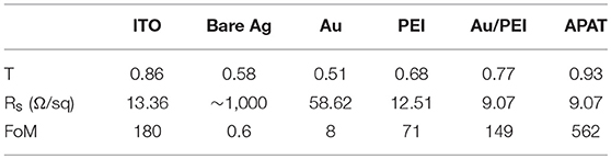
Table 2. Optical and electrical parameters of transmittance, sheet resistance, and FoM obtained from different TCEs.
Apart from the optoelectronic properties, the long-term environmental stability and mechanical flexibility of the APAT film also play indispensable roles in the evaluation of the resultant FTCEs. The stability of Rsheet of the APAT film was investigated as a function of time by exposing the film to ambient environment. As shown in Figure 4A, the Rsheet of the bare Ag dramatically increased after exposing to ambient environment for 48 h, which is possibly due to the chemical corrosion of Ag through oxidation or sulfidation reactions (Graedel, 1992). After capping with the Ta2O5 layer, the Rsheet of the APAT film increased only by ~0.5% under the same condition, suggesting that the Ta2O5 layer can effectively protect the Ag underlayer. Meanwhile, the mechanical robustness of the APAT film was evaluated by conducting a bending test, and that of the ITO was estimated for comparison. Figure 4B shows the changes in the Rsheet of APAT and ITO films on PET substrates as a function of bending radius. Figure 4C shows the photograph of an optimized APAT film fabricated on an 8 in flexible PET. The APAT film shows a negligible increase in the Rsheet at a bending radius of 6 mm. In contrast, the ITO film shows a dramatic increase in Rsheet even as the bending radius is decreased to 8 mm. Moreover, the reliability of the TEs in terms of mechanical deformation geometries under continuous exposures to repeated bending was investigated by performing a repeated bending test with a 9 mm radius of curvature. As seen in Figure 4D, the Rsheet of ITO increases dramatically as soon as the bending test is initiated due to its inherent brittleness. In comparison, the APAT exhibits a Rsheet change of <2% even after 700 bending cycles and no crack appears on the film surface; this indicates the excellent mechanical flexibility of the APAT-based FTCEs.
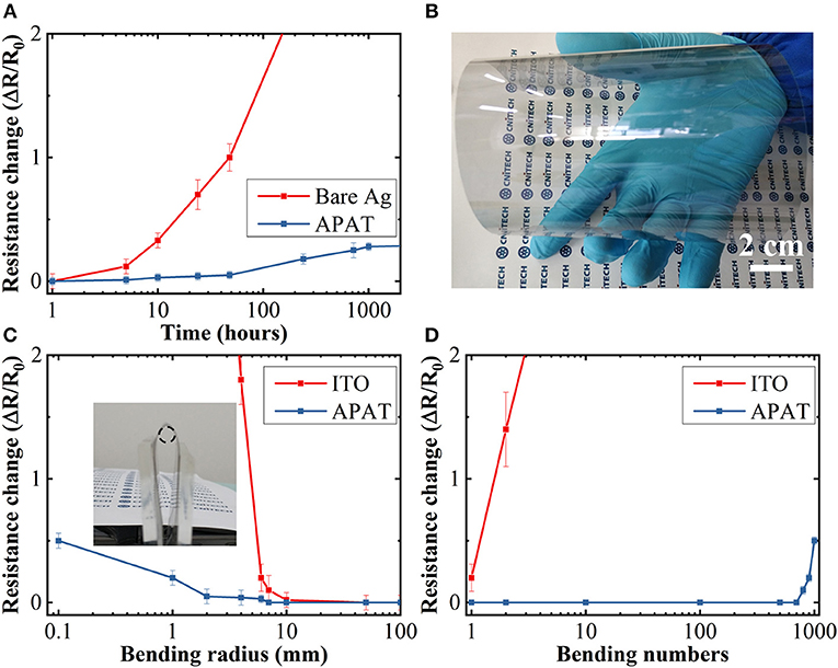
Figure 4. (A) Relative changes in the resistance of bare Ag and APAT film as a function of exposure time of up to 1,000 h. (B) Photograph of an 8 in flexible APAT film on PET. Relative change in the resistances of ITO and APAT films as a function of (C) bending radius and (D) number of bending cycles at a bending radius of 9 mm. The inset in (C) shows a photograph of a folded APAT film with a bending radius of 2 mm set for the bending test.
Conclusion
In summary, a high-performance UTAF with a percolation threshold thickness of as low as 3 nm is successfully demonstrated by incorporating an Au/PEI bilayered structure as a novel NISL with a high density of nucleation sites for the incoming deposited Ag atoms. XPS studies revealed that the adsorbed PEI monomers on Au precoated layer are immobilized by a strong coordination reaction between amine groups and Au atoms rather than the weak electrostatic interaction in the conventional adsorption of PEI without Au. Benefitting from the increased PEI density, the Ag film deposited on Au/PEI bilayered NISL shows a much smoother surface morphology as well as a higher conductivity and lower optical absorption loss than those of the Ag films deposited on conventional single-layered Au and PEI NISLs. After capping with a high-refractive-index Ta2O5 anti-reflection layer, a Rsheet of 9.07 Ω/sq and T of 92.9% at a wavelength of 550 nm are achieved for the resultant APAT stacked film. In addition, the APAT-based FTCE exhibits excellent long-term environmental and mechanical stabilities. Our work paves a facile way for the development of high-density NISLs for efficient UTMF-based FTCEs, which have a substantial application in flexible electronics.
Author Contributions
XY, BY, and JY designed experiments. ZW, ZY, and WG carried out experiments. LL, NL, EJ, and JZ analyzed experimental results. XY and ZW wrote the manuscript.
Conflict of Interest Statement
The authors declare that the research was conducted in the absence of any commercial or financial relationships that could be construed as a potential conflict of interest.
Acknowledgments
This work was supported by the National Natural Science Foundation of China (Grant No. 51601210, 61874177, 61704176), Zhejiang Provincial Natural Science Foundation of China (Grant No. LR16F040002).
Abbreviations
UTAF, ultrathin Ag film; ITO, indium tin oxide; NISL, nucleation inducing seed layer; PEI, polyethyleneimine; Ta2O5, Tantalum pentoxide; APAT, Au/PEI/Ag/Ta2O5; FTCEs, flexible transparent conductive electrodes; T, transmittance; Rsheet, sheet resistance; UTMFs, ultrathin metal films; SEM, scanning electron microscopy; AFM, atomic force microscope; XPS, X-ray photoelectron spectroscopy; BE, binding energy; RMS, root-mean-square; SPR, surface plasmon resonance; FoM, figure of merit.
References
Chang, C.-Y., Chang, Y.-C., Huang, W.-K., Liao, W.-C., Wang, H., Yeh, C., et al. (2016). Achieving high efficiency and improved stability in large-area ITO-free perovskite solar cells with thiol-functionalized self-assembled monolayers. J. Mater. Chem. A. 4, 7903–7913. doi: 10.1039/C6TA02581A
Daniel, M.-C., and Astruc, D. (2004). Gold nanoparticles: assembly, supramolecular chemistry, quantum-size-related properties, and applications toward biology, catalysis, and nanotechnology. Chem. Rev. 104, 293–346. doi: 10.1021/cr030698+
Dobrynin, A. V., Deshkovski, A., and Rubinstein, M. (2000). Adsorption of polyelectrolytes at an oppositely charged surface. Phys. Rev. Lett. 84, 3101–3104. doi: 10.1103/PhysRevLett.84.3101
Ellmer, K. (2012). Past achievements and future challenges in the development of optically transparent electrodes. Nat. Photonics 6, 809–817. doi: 10.1038/nphoton.2012.282
Ghosh, D. S. (2012). Ultrathin Metal Transparent Electrodes for the Optoelectronics Industry. Heidelberg: Springer.
Ghosh, D. S., and Leo, K. (2017). Microcavity-enhanced semitransparent electrodes for oligothiophene small-molecule organic solar cells. Adv. Electronic Mater. 3:1600518. doi: 10.1002/aelm.201600518
Gorin, D. A., Yashchenok, A. M., Manturov, A. O., Kolesnikova, T. A., and Möhwald, H. (2009). Effect of layer-by-layer electrostatic assemblies on the surface potential and current voltage characteristic of metal–insulator–semiconductor structures. Langmuir 25, 12529–12534. doi: 10.1021/la901379d
Graedel, T. E. (1992). Corrosion mechanisms for silver exposed to the atmosphere. J. Electrochem. Soc. 139, 1963–1970. doi: 10.1149/1.2221162
Guo, C. F., Sun, T., Liu, Q., Suo, Z., and Ren, Z. (2013). Highly stretchable and transparent nanomesh electrodes made by grain boundary lithography. Nat. Commun. 5, 155–164. doi: 10.1038/ncomms4121
Hatton, R. A., Willis, M. R., Chesters, M. A., and Briggs, D. (2003). A robust ultrathin, transparent gold electrode tailored for hole injection into organic light-emitting diodes. J. Mater. Chem. 13, 722–726. doi: 10.1039/b211775b
Hecht, D. S., Hu, L., and Irvin, G. (2011). Emerging transparent electrodes based on thin films of carbon nanotubes, graphene, and metallic nanostructures. Adv. Mater. 23, 1482–1513. doi: 10.1002/adma.201003188
Hoogeveen, N. G., Stuart, M. A. C., and Fleer, G. J. (1996). Polyelectrolyte adsorption on oxides: i. kinetics and adsorbed amounts. J. Colloid Interface Sci. 182, 133–145. doi: 10.1006/jcis.1996.0444
Hsu, P. C., Wang, S., Wu, H., Narasimhan, V. K., Kong, D. S., Ryoung Lee, H., et al. (2013). Performance enhancement of metal nanowire transparent conducting electrodes by mesoscale metal wires. Nat. Commun. 4, 2522–2528. doi: 10.1038/Ncomms3522
Hutter, O. S., and Hatton, R. A. (2015). A hybrid copper:tungsten suboxide window electrode for organic photovoltaics. Adv. Mater. 27, 326–331. doi: 10.1002/adma.201404263
Hutter, O. S., Stec, H. M., and Hatton, R. A. (2013). An indium-free low work function window electrode for organic photovoltaics which improves with in-situ oxidation. Adv. Mater. 25, 284–288. doi: 10.1002/adma.201203280
Illhwan, L., and Jong-Lam, L. (2015). Transparent electrode of nanoscale metal film for optoelectronic devices. J. Photonics Energy 5:057609. doi: 10.1117/1.JPE.5.057609
Jeong, J.-A., and Kim, H.-K. (2013). Al2O3/Ag/Al2O3 multilayer thin film passivation prepared by plasma damage-free linear facing target sputtering for organic light emitting diodes. Thin Solid Films 547, 63–67. doi: 10.1016/j.tsf.2013.05.003
Jeong, S., Jung, S., Kang, H., Lee, D., Choi, S. B., Kim, S., et al. (2017). Role of polymeric metal nucleation inducers in fabricating large-area, flexible, and transparent electrodes for printable electronics. Adv. Funct. Mater. 27:1606842. doi: 10.1002/adfm.201606842
Kang, H., Jung, S., Jeong, S., Kim, G., and Lee, K. (2015). Polymer-metal hybrid transparent electrodes for flexible electronics. Nat. Commun. 6, 6503–6509. doi: 10.1038/ncomms7503
Kim, S., Cho, H. W., Hong, K., Son, J. H., Kim, K., Koo, B., et al. (2014). Design of red, green, blue transparent electrodes for flexible optical devices. Opt. Express 22, A1257–A1269. doi: 10.1364/OE.22.0A1257
Li, D., Lütt, M., Shi, X., and Fitzsimmons, M. R. (1997). Multilayer self-assemblies as electronic and optical materials. MRS Proc. 488, 401–406. doi: 10.1557/PROC-488-401
Liu, H., Wang, B., Leong, E. S. P., Yang, P., Zong, Y., Si, G., et al. (2010). Enhanced surface plasmon resonance on a smooth silver film with a seed growth layer. ACS Nano 4, 3139–3146. doi: 10.1021/nn100466p
Logeeswaran, V. J., Kobayashi, N. P., Islam, M. S., Wu, W., Chaturvedi, P., Fang, N. X., et al. (2009). Ultrasmooth silver thin films deposited with a germanium nucleation layer. Nano Lett. 9, 178–182. doi: 10.1021/nl8027476
Luo, G., Cheng, X., He, Z., Wu, H., and Cao, Y. (2014). High-performance inverted polymer solar cells based on thin copper film. J. Photonics Energy 5:057206. doi: 10.1117/1.jpe.5.057206
Maniyara, R. A., Mkhitaryan, V. K., Chen, T. L., Ghosh, D. S., and Pruneri, V. (2016). An antireflection transparent conductor with ultralow optical loss (< 2 %) and electrical resistance (< 6 Ω sq−1). Nat. Commun. 7, 13771–13778. doi: 10.1038/ncomms13771
Meiss, J., Allinger, N., Riede, M. K., and Leo, K. (2008). Improved light harvesting in tin-doped indum oxide (ITO)-free inverted bulk-heterojunction organic solar cells using capping layers. Appl. Phys. Lett. 93:103311. doi: 10.1063/1.2981525
Min, X., Jiang, F., Qin, F., Li, Z., Tong, J., Xiong, S., et al. (2014). Polyethylenimine aqueous solution: a low-cost and environmentally friendly formulation to produce low-work-function electrodes for efficient easy-to-fabricate organic solar cells. ACS Appl. Mater. Interfaces 6, 22628–22633. doi: 10.1021/am5077974
Morales-Masis, M., De Wolf, S., Woods-Robinson, R., Ager, J. W., and Ballif, C. (2017). Transparent electrodes for efficient optoelectronics. Adv. Electronic Mater. 3:1600529. doi: 10.1002/aelm.201600529
Nair, R., Blake, P., Grigorenko, A., Novoselov, K., Booth, T., Stauber, T., et al. (2008). Fine structure constant defines visual transparency of graphene. Science 320, 1308–1308. doi: 10.1126/science.1156965
Ricciardulli, A. G., Yang, S., Wetzelaer, G.-J. A. H., Feng, X., and Blom, P. W. M. (2018). Hybrid silver nanowire and graphene-based solution-processed transparent electrode for organic optoelectronics. Adv. Funct. Mater. 28:1706010. doi: 10.1002/adfm.201706010
Salinas, J. F., Yip, H. L., Chueh, C. C., Li, C. Z., Maldonado, J. L., and Jen, A. K. Y. (2012). Optical design of transparent thin metal electrodes to enhance in-coupling and trapping of light in flexible polymer solar cells. Adv. Mater. 24, 6362–6367. doi: 10.1002/Adma.201203099
Schubert, S., Meiss, J., Müller-Meskamp, L., and Leo, K. (2013). Improvement of transparent metal top electrodes for organic solar cells by introducing a high surface energy seed layer. Adv. Energy Mater. 3, 438–443. doi: 10.1002/aenm.201200903
Schubert, S., Müller-Meskamp, L., and Leo, K. (2014). Unusually high optical transmission in ca:ag blend films: high-performance top electrodes for efficient organic solar cells. Adv. Funct. Mater. 24, 6668–6676. doi: 10.1002/adfm.201401854
Stec, H. M., Williams, R. J., Jones, T. S., and Hatton, R. A. (2011). Ultrathin transparent au electrodes for organic photovoltaics fabricated using a mixed mono-molecular nucleation layer. Adv. Funct. Mater. 21, 1709–1716. doi: 10.1002/adfm.201002021
Suriyanarayanan, S., Lee, H.-H., Liedberg, B., Aastrup, T., and Nicholls, I. A. (2013). Protein-resistant hyperbranched polyethyleneimine brush surfaces. J. Colloid Interface Sci. 396, 307–315. doi: 10.1016/j.jcis.2012.12.076
Wang, J., Chen, X., Jiang, F., Luo, Q., Zhang, L., Tan, M., et al. (2018). Electrochemical corrosion of ag electrode in the silver grid electrode-based flexible perovskite solar cells and the suppression method. Solar RRL 2:1800118. doi: 10.1002/solr.201800118
Wang, W., Song, M., Bae, T.-S., Park, Y. H., Kang, Y.-C., Lee, S.-G., et al. (2014). Transparent ultrathin oxygen-doped silver electrodes for flexible organic solar cells. Adv. Funct. Mater. 24, 1551–1561. doi: 10.1002/adfm.201301359
Xu, G., Tazawa, M., Jin, P., Nakao, S., and Yoshimura, K. (2003). Wavelength tuning of surface plasmon resonance using dielectric layers on silver island films. Appl. Phys. Lett. 82, 3811–3813. doi: 10.1063/1.1578518
Xue, Q., Bai, Y., Liu, M., Xia, R., Hu, Z., Chen, Z., et al. (2016). Dual interfacial modifications enable high performance semitransparent perovskite solar cells with large open circuit voltage and fill factor. Adv. Energy Mater. 7:1602333. doi: 10.1002/aenm.201602333
Yang, X., Gao, P., Yang, Z., Zhu, J., Huang, F., and Ye, J. (2017). Optimizing ultrathin Ag films for high performance oxide-metal-oxide flexible transparent electrodes through surface energy modulation and template-stripping procedures. Sci. Rep. 7, 44576–44584. doi: 10.1038/srep44576
Yu, L.-L., Tao, S.-P., Dong, X.-Y., and Sun, Y. (2013). Protein adsorption to poly(ethylenimine)-modified Sepharose FF: I. A critical ionic capacity for drastically enhanced capacity and uptake kinetics. J. Chromatogr. A 1305, 76–84. doi: 10.1016/j.chroma.2013.07.014
Yun, J. (2017). Ultrathin metal films for transparent electrodes of flexible optoelectronic devices. Adv. Funct. Mater. 27:1606641. doi: 10.1002/adfm.201606641
Zhang, C., Zhao, D., Gu, D., Hyunsoo, K., Ling, T., Wu, Y. K. R., et al. (2014). An Ultrathin, smooth, and low-loss al-doped ag film and its application as a transparent electrode in organic photovoltaics. Adv. Mater. 26, 5696–5701. doi: 10.1002/adma.201306091
Zhang, L., Persaud, R., and Madey, T. E. (1997). Ultrathin metal films on a metal oxide surface: Growth of Au on TiO2 (110). Phys. Rev. B 56, 10549–10557. doi: 10.1103/PhysRevB.56.10549
Zhang, M., Fang, S., Zakhidov, A. A., Lee, S. B., Aliev, A. E., Williams, C. D., et al. (2005). Strong, transparent, multifunctional, carbon nanotube sheets. Science 309, 1215–1219. doi: 10.1126/science.1115311
Zheng, W., Lin, Y., Zhang, Y., Yang, J., Peng, Z., Liu, A., et al. (2017). Dual Function of UV/Ozone plasma-treated polymer in polymer/metal hybrid electrodes and semitransparent polymer solar cells. ACS Appl. Mater. Interfaces 9, 44656–44666. doi: 10.1021/acsami.7b14395
Zhu, J., Yang, X., Yang, Z., Wang, D., Gao, P., and Ye, J. (2018). Achieving a record fill factor for silicon–organic hybrid heterojunction solar cells by using a full-area metal polymer nanocomposite top electrode. Adv. Funct. Mater. 28:1705425. doi: 10.1002/adfm.201705425
Keywords: flexible transparent conductive electrodes, ultra-thin metal film, nucleation inducing seed layer, bilayer, tantalum pentoxide, polyethyleneimine
Citation: Wang Z, Yang X, Yang Z, Guo W, Lin L, Li N, Jiang E, Zhang J, Yan B and Ye J (2019) Metal-Enhanced Adsorption of High-Density Polyelectrolyte Nucleation-Inducing Seed Layer for Highly Conductive Transparent Ultrathin Metal Films. Front. Mater. 6:18. doi: 10.3389/fmats.2019.00018
Received: 14 November 2018; Accepted: 30 January 2019;
Published: 22 February 2019.
Edited by:
Jinn P. Chu, National Taiwan University of Science and Technology, TaiwanReviewed by:
Manuel Pereira Dos Santos, Universidade de Évora, PortugalYantao Shi, Dalian University of Technology (DUT), China
Copyright © 2019 Wang, Yang, Yang, Guo, Lin, Li, Jiang, Zhang, Yan and Ye. This is an open-access article distributed under the terms of the Creative Commons Attribution License (CC BY). The use, distribution or reproduction in other forums is permitted, provided the original author(s) and the copyright owner(s) are credited and that the original publication in this journal is cited, in accordance with accepted academic practice. No use, distribution or reproduction is permitted which does not comply with these terms.
*Correspondence: Xi Yang, eWFuZ3hAbmltdGUuYWMuY24=
Jianfeng Zhang, empmQG5idS5lZHUuY24=
Jichun Ye, amljaHVuLnllQG5pbXRlLmFjLmNu