 Huong Tran1
 Callum G. Littlejohns2
 David J. Thomson2
 Thach Pham1
 Amir Ghetmiri3
 Aboozar Mosleh3Joe Margetis4John Tolle4
 Goran Z. Mashanovich2
 Wei Du5Baohua Li6
 Mansour Mortazavi3
 Shui-Qing Yu1*
- 1Department of Electrical Engineering, University of Arkansas, Fayetteville, AR, United States
- 2Optoelectronics Research Centre, University of Southampton, Southampton, United Kingdom
- 3Department of Chemistry and Physics, University of Arkansas at Pine Bluff, Pine Bluff, AR, United States
- 4ASM, Phoenix, AR, United States
- 5Department of Electrical Engineering, Wilkes University, Wilkes-Barre, PA, United States
- 6Arktonics LLC, Fayetteville, AR, United States
In 2016, Thach et al. reported figures of merit of the GeSn photodiodes with large mesa sizes of 500 and 250 μm to show the potential of the GeSn materials in short-wave infrared photonics23. However, there are only a few discussions about high frequency capabilities of GeSn photodetectors. It is needed to understand the potential of GeSn detectors as high frequency devices. This paper discusses comprehensively about the performance of GeSn photodiodes with 6.44 and 9.24% Sn for high frequency applications including high speed measurements and simulations. With high Sn incorporation, the cutoff wavelength is extended up to 2.2 and 2.5 μm wavelengths for 6.44 and 9.24% Sn devices, respectively. The photodiodes' bandwidth is 1.78 GHz, and the simulation shows excellent agreement with measurement results. The reported GeSn photodetectors together with recently reported GeSn lasers and other GeSn microwave photonic components will be a potential candidate for integrated microwave photonics.
Introduction
Silicon-based photonic components are especially attractive for realizing low-cost photonic integrated circuits using large-scale manufacture (Thomson et al., 2016). Microwave photonics (MWP) not only marries the fields of the radiofrequency (RF) engineering and optoelectronics, but also brings in a considerable added value to traditional microwave and RF systems. Integrated Microwave Photonics (IMWP) incorporates the functions of MWP components in monolithic or hybrid photonic circuits (Capmany and Novak, 2007). Hence, IMWP offers the promise of reduction of size-weight-and-power (SWAP) and low-cost of production. Moreover, the traditional MWP platform has confronted the two-photon absorption issue. It requires a shift of the working wavelength to 2 μm and beyond in order for it to be utilized in MWP applications (Capmany et al., 2013; Liu et al., 2016; Zhang and Yao, 2016). In addition, a monolithic integrated solution combining high-performance light sources and detectors, low loss passive devices, and complementary metal-oxide-semiconductor (CMOS) and RF circuits on a single platform with operating wavelength beyond 2 μm is also a challenge (Soref, 2008; Roelkens et al., 2013; Hagan et al., 2019).
Recently, Silicon-germanium-tin (SiGeSn) and Germanium-tin (GeSn) techniques have drawn much attention due to the success of developing all-group-IV alloy with outstanding material properties including (i) independent tuning of the lattice constant and bandgap by simultaneously varying the compositions of Si, Ge, and Sn (Jenkins and Dow, 1987); (ii) true direct-bandgap material (Zhou et al., 2019); (iii) wavelength coverage up to 12 μm (Du et al., 2016); and (iv) a low material growth temperature fully compatible with CMOS processes (Grant et al., 2019). The advantages of a SiGeSn approach are (i) compatibility with the proven high-performance Silicon on Insulator (SOI) passive and Electro-optic (EO) components, and (ii) enhanced dynamic range as two-photon absorption at 1.55 μm in Si under high laser power operation is effectively suppressed by shifting the operating wavelength to 2 μm and beyond (Cao et al., 2018). Hence, SiGeSn and GeSn materials are strong candidates for the monolithic silicon-based factory-compatible integrated photonics technology with high-performance for Si-based digital/RF photonics link for operation at 2 μm wavelength and beyond.
Over the last 10 years, many GeSn-based photodetectors have been reported with their performance dramatically improved. The responsivity of photodetectors keeps increasing as well as more Sn incorporation in the materials, which extends cut-off wavelength to mid-infrared ranges (Mathews et al., 2009; Su et al., 2011; Werner et al., 2011; Kim et al., 2013; Tseng et al., 2013; Zhang et al., 2013; Peng et al., 2014; Dong et al., 2015; Chang et al., 2016; Pham et al., 2016; Huang et al., 2017; Tran et al., 2018). However, only a few reports are available discussing the high-speed capability of the GeSn photodetectors (Oehme et al., 2014; Dong et al., 2017; Xu et al., 2019). It is highly desired to fully understand the potential of GeSn detectors as high frequency devices for the 2 μm wavelength range and beyond. In this work, we report comprehensive studies of 6.44 and 9.24% Sn photodiodes to demonstrate high frequency functionality. The cutoff wavelengths are extended beyond 2 μm. The measured bandwidths of the devices achieve 1.78 GHz, while the bitrate is 1 Gbit/s. The simulation shows excellent agreement with measurement results. Further simulation has indicated that a reduction of the mesa diameter could increase the bandwidth to one order of magnitude higher than that of the reported devices.
Experimental Methods
Growth and Fabrication
The GeSn double heterostructure (DHS) samples were grown using an industry standard ASM Epsilon® 2000 Plus reduced pressure chemical vapor deposition system (RPCVD) with SnCl4 and GeH4 as Sn and Ge precursors, respectively. A 750-nm-thick p-type (Boron as dopant) Ge buffer was first grown on the Si substrate. Then, a 200-nm-thick (unintentionally doped) GeSn layer was grown followed by a 50-nm-thick n-type (Arsenic as the dopant) Ge cap layer. The GeSn layer has a background doping level of 1 × 1017 cm−3, while the doping concentration at Ge buffer and Ge cap layer were 5 × 10¹⁸ and 1 × 1019 cm−3, respectively. The details of the growth technique have been published elsewhere (Margetis et al., 2019). The X-ray diffraction (XRD) shows Sn compositions of 6.44 and 9.24%, corresponding to nominal 7 and 10% Sn, respectively. The detailed analysis of XRD data was published elsewhere (Zhou et al., 2016).
Circular mesa structures with diameters of 500, 250, and 100 μm were defined by standard photolithography and then etched using wet chemical etching process. The solution of HCl: H2O2: H2O = 1:1:20 was used in the process. To determine the etching rate, several testing samples were etched with different etch time. A stable etching rate of 100 nm/min at room temperature regardless of Sn composition was observed. The mesas were etched until the p-type Ge buffer was reached. A 100-nm-thick SiO2 passivation layer was then deposited by plasma-enhanced chemical vapor deposition. The oxide was opened to form the metal contacts. Electrode pads were patterned and metalized with 10/200 nm of Cr/Au. Figure 1a shows the top-view scanning electron microscope (SEM) image using FEI- XL30 Environmental Scanning Electron Microscope. The schematic of device cross-sectional view is plotted in Figure 1a inset. The cross-sectional SEM image (see Figure 1b) shows clearly resolved Ge and GeSn layers with defects trapped near GeSn/Ge and Ge/Si interfaces.
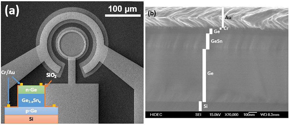
Figure 1. (a) The top-view SEM image of the typical device (Inset) its cross-sectional view. (b) Cross-section SEM image.
Measurement
The dark current-voltage characteristics were measured with a direct current (DC) source (Keithley 236 Source Measurement Unit). The temperature-dependent spectral response of the devices was conducted using a Fourier-transform infrared (FTIR) (Nicolet 8700 FTIR spectrometer) spectrometer at a bias of −2 V. The devices' responsivity was measured using a 1.55 μm laser diode (Thorlabs ML925B45F) as a light source, a chopper at 380 Hz and a lock-in amplifier (Stanford Research SR830). The power of the light sources from the FTIR and the laser diode were calibrated using the pre-calibrated InGaAs and extended-InGaAs detectors under the same ambience conditions.
For the high frequency measurements, the detectors' electrical bandwidth and eye diagrams were conducted. Using a network analyzer (N5225A-200), port one was connected to the RF input of a fiber coupled lithium niobate modulator (model MX-2000-LN-10) rated for 10 GHz. A 2 μm laser diode fed the optical input of the modulator, with the optical output passed to the surface of the detector via a lensed fiber. The electrical pads of the detector were contacted with an RF probe, with the electrical signal passed through a bias tee to port 2 of the network analyzer. The bias tee was used to allow a DC bias to be applied to the detector.
Figure 2 shows 2 μm high speed setup to gather the eye diagrams. The light source used was a fiber coupled laser diode with a wavelength of 1.963 μm. A home-built thulium doped optical fiber amplifier (TDFA) (Li et al., 2013) was used to boost input power prior to the LiNbO3 modulator. A polarization controller and PM2000 lensed fiber connected to the output of the modulator was used to vertically couple light into the device under test (DUT) mounted on a piezoelectric xyz stage. The modulator was driven by a 1 Gbps bit pattern generator with an RF amplifier rated for up to 40 Gbps operation.
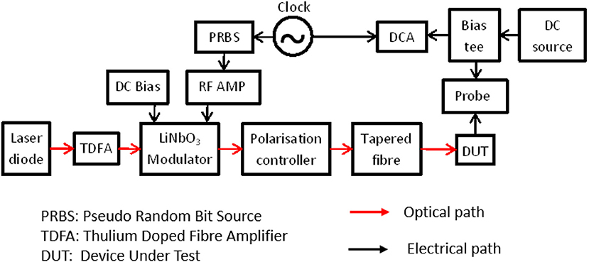
Figure 2. A schematic of the experimental setup to obtain eye diagrams at 2 μm.
The photodetector was interfaced with a 40 GHz RF probe with a ground-signal contact configuration. A picoseconds pulse labs model 5543 bias tee rated at 50 GHz was used to apply bias using a source meter. The AC signal was sent do a digital communications analyzer with electrical input rated for 80 GHz.
Simulation
The devices were simulated using the commercial Silvaco software with Atlas simulator. The three basic semiconductor equations such as Poisson, carrier continuity, and transport equations were solved1. The detectors were modeled using a pseudo-3D method which assumes that they have cylindrical geometry and symmetry by defining cylindrical mesh. The material models were default Ge material, but the bandgap, effective density of states and intrinsic carrier concentration were modified for GeSn materials. The drift-diffusion transport model was used with field dependent mobility. The Shockley-Read-Hall (SRH) recombination model was used with electron and hole lifetimes of 1 ns (Elbaz et al., 2018). Surface recombination on the devices' surfaces and sidewalls was considered with the recombination velocities of 105 cm/s for electrons and holes (McEvoy et al., 2012). The default refractive index and extinction coefficient of the Ge were overwritten using data that were measured by ellipsometry for the GeSn materials to simulate the devices under illumination (Tran et al., 2016). The intensity that is assumed to be uniform across the width of the beam has a density of 0.01 W/cm2.
Results and Discussion
The simulated (solid points) and measured (curves) current density-voltage (J-V) characteristics are shown in Figure 3 for the Ge0.9356Sn0.0644 and Ge0.9076Sn0.0924 photodiodes. Under forward bias, where the series resistance is dominant, a good agreement between the experimental and simulated data for the forward bias was observed. At the zero bias voltage, the shunt resistance originally from surface leakage current becomes a dominant factor. At higher reverse bias, the SRH recombination becomes more effective than the others. Because of the lattice mismatch between Ge buffer and GeSn materials, the GeSn/Ge interface is defective, which might be the main reason for the relative high dark current. In the SRH model to represent the defective layers, short carrier lifetimes are also considered. At a certain reverse voltage, the current density of the 9.24% Sn device is higher than that of the 6.44% Sn device. Because the bandgap of the 9.24% Sn device is narrower than that of the 6.44% Sn device, which leads to the 9.24% Sn device having higher intrinsic carrier concentration. Moreover, there is deviation between the measurement and simulation for 6.44% Sn device at small reverse bias from −0.4 V to −0.1 V, shown in Figure 3A. The measured dark current may be limited by diffusion current, which leads to lower values comparing with the simulated current, in which we assumed SRH is a dominant mechanism.
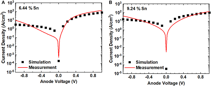
Figure 3. Simulated and measured J-V characteristics of (A) the Ge0.9356Sn0.0644 device and (B) the Ge0.9076Sn0.0924 device.
Figure 4 shows the simulated and measured spectral response of (a) 6.44% and (b) 9.24% Sn photodiode detectors. The 6.44% Sn device exhibits a cutoff wavelength of 2.2 μm. The cutoff wavelength is much longer than the Ge band-to-band absorption edge (1.55 μm), indicating major photo response contribution is from GeSn layer. For the 9.24% Sn device, the spectral response is extended to 2.5 μm. This longer wavelength coverage is due to the reduced bandgap for the increased Sn composition as expected. The simulated results match the measured ones, which indicates that the GeSn material models are valid. It is worth noting that the devices' spectral response not only covers the traditional L- and C-band, but also the 2 μm telecommunication band.
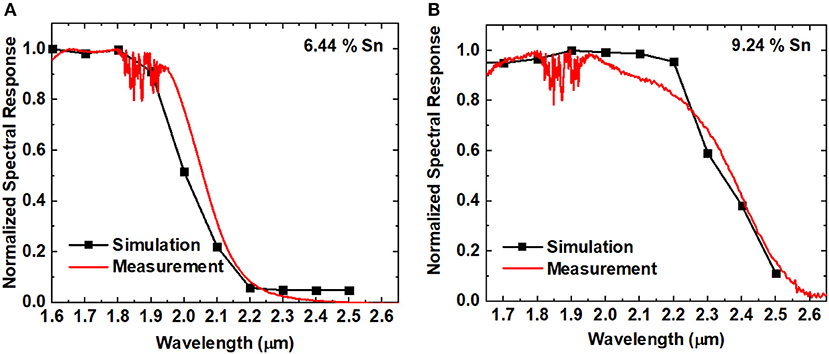
Figure 4. Spectral response of (A) the Ge0.9356Sn0.0644 device and (B) the Ge0.9076Sn0.0924 device.
The responsivity at 1.55 μm of the 6.44 and 9.24% Sn photodiode devices are shown in Figures 5A,B, respectively. Peak responsivities of 0.12 and 0.19 A/W were obtained with a 0.1 V reverse bias voltage for the 6.44 and 9.24% Sn samples, respectively. As the reverse bias voltage increases, the responsivity decreases. This responsivity reduction is possibly associated with the Franz-Keldysh effect (Pham et al., 2016; Lin and Chang, 2018; Tran et al., 2018). At a 1 V reverse bias voltage, the responsivities reduce to 0.08 and 0.07 A/W for the 6.44 and 9.24% Sn devices, respectively. Since the simulation cannot take the Franz-Keldysh effect into account, the simulated responsivity shows independent behaviors with bias voltage (not shown here), and it is inaccurate. Moreover, the responsivity of both devices show similar values, suggesting that the material qualities are comparable.
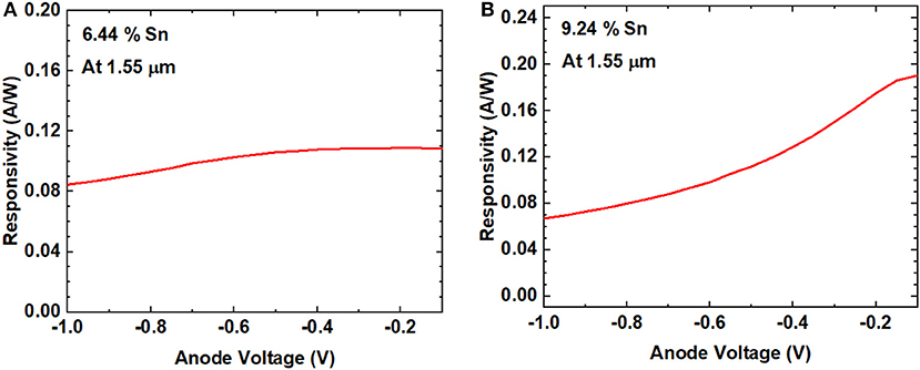
Figure 5. Responsivity measured at 1.55 μm of the (A) 6.44% Sn and (B) 9.24% Sn devices.
High frequency performances of the GeSn devices with different mesa sizes of 500, 250, and 100 μm at different applied voltages were summarized in Table 1. The operation bandwidth increases as the mesa size decreases, which is due to reduction of junction resistance-capacitance. As the reverse bias voltage increases, the depletion width increases, which also increases the bandwidth of the devices. The RF response of the GeSn devices with mesa's diameter of 100 μm are shown in Figure 6, while the simulated results are shown in the inset. The frequency response at −6 dB bandwidth is 1.78 GHz at −7 V bias, while the simulations of optical bandwidth at −3 dB show 2 GHz measured at 2 μm and −7 V bias. In general, the bandwidths of the devices depend on the two significant factors: (i) the carrier lifetime, and (ii) the junction resistance-capacitance. The devices' dimensions were not optimized in this work. In order to achieve much higher bandwidth for the devices, the devices' size needs to be reduced. In further simulation, the simulated −3 dB bandwidth of the 10 μm diameter device was 10 GHz which was almost one order of magnitude higher than that of the 100 μm mesa device. The frequency response achieved at 2 GHz indicates the great potential of GeSn photodiodes for high-speed applications in MWP.
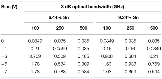
Table 1. Bandwidth of the GeSn devices with different mesa sizes and at different bias voltages.
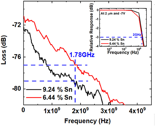
Figure 6. Electrical bandwidth of 1.78 GHz for both devices with mesa's diameter of 100 μm; (inset) simulated results for optical bandwidth of 2 GHz for both devices.
Figure 7 shows a 1 Gbit/s eye diagram obtained from the 6.44% Sn device. The bit rate is lower than the bandwidth. It is worth noting that there may be a pitfall of relying on the bandwidth value for evaluating the time-domain performance. In fact, the behavior of the system in the frequency-domain (i.e., the slope in the frequency domain) is also important. However, the determination of the bandwidth at −3 dB is still valid in the case of the steeper slope of the frequency response.
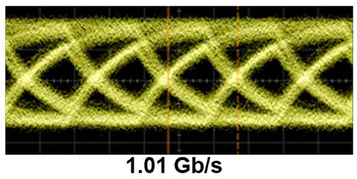
Figure 7. Eye diagram of the 6.44% Sn device.
Conclusions
In summary, systematic studies of Ge0.9356Sn0.0644 and Ge0.9076Sn0.0924 photodiodes were conducted. Detection of the reported 6.44 and 9.24% Sn devices are up to 2.2 and 2.5 μm wavelengths, respectively. The measured bandwidths of the devices achieve 1.78 GHz, while the bitrate is 1 Gbit/s. Moreover, in the further simulation, the reduction of the mesa diameter could increase the bandwidth. The detection wavelengths can be extended to the mid- and far-infrared as more Sn is incorporated into the materials. The current GeSn photodetectors, together with the recently reported GeSn lasers and other GeSn microwave photonic components (i.e., high-speed modulator and waveguide) will be a potential candidate for integrated microwave photonic applications.
Data Availability Statement
All datasets generated for this study are included in the article/supplementary material.
Author Contributions
S-QY, GM, MM, BL, and WD proposed and guided the overall project. JM and JT planned and conducted GeSn epitaxial growths and performed material characterization. HT and TP fabricated photodetector devices, developed, conducted, and analyzed photodetector measurements. CL and DT setup and performed high frequency measurements. HT modeled and conducted simulations. All authors discussed the results and commented on the manuscript.
Funding
This work was supported by the Air Force Office of Scientific Research (AFOSR) (Grant No. FA9550-18-1-0361) and the National Aeronautics and Space Administration Established Program to Stimulate Competitive Research (NASA EPSCoR) (Grant No. NNX15AN18A).
Conflict of Interest
BL was employed by company Arktonics. JM and JT were employed by company ASM.
The remaining authors declare that the research was conducted in the absence of any commercial or financial relationships that could be construed as a potential conflict of interest.
Acknowledgments
The authors acknowledge financial support from the Air Force Office of Scientific Research (AFOSR) (Grant No. FA9550-18-1-0361) and the National Aeronautics and Space Administration Established Program to Stimulate Competitive Research (NASA EPSCoR) (Grant No. NNX15AN18A). WD appreciates support from Provost's Research and Scholarship Fund at Wilkes University. DT and GM acknowledge funding from the Royal Society for their University Research Fellowships. We are thankful for Dr. M. Benamara's assistance in TEM imaging and Dr. A. Kuchuk's assistance in XRD measurement from Institute for Nanoscience and Engineering, University of Arkansas.
Footnotes
1. ^Atlas User's Manual, June 2019, [online] available: http://www.Silvaco.com.
References
Cao, W., Hagan, D., Thomson, D. J., Nedeljkovic, M., Littlejohns, C. G., Knights, A., et al. (2018). High-speed silicon modulators for the 2 μm wavelength band. Optica 5, 1055–1062. doi: 10.1364/OPTICA.5.001055
Capmany, J., Li, G., Lim, C., and Yao, J. (2013). Microwave photonics: current challenges towards widespread application. Opt. Express 21, 22862–22867. doi: 10.1364/OE.21.022862
Capmany, J., and Novak, D. (2007). Microwave photonics combines two worlds. Nat. Photon. 1, 319–330. doi: 10.1038/nphoton.2007.89
Chang, C., Li, H., Huang, S. H., Cheng, H. H., Sun, G., and Soref, R. A. (2016). Sn-based Ge/Ge0.975Sn0.025/Ge p-i-n photodetector operated with back-side illumination. Appl. Phys. Lett. 108:151101. doi: 10.1063/1.4945816
Dong, Y., Wang, W., Lei, D., Gong, X., Zhou, Q., Lee, S. Y., et al. (2015). Suppression of dark current in germanium-tin on silicon p-i-n photodiode by a silicon surface passivation technique. Opt. Express 23:18611. doi: 10.1364/OE.23.018611
Dong, Y., Wang, W., Xu, S., Lei, D., Gong, X., Guo, X., et al. (2017). Two-micron-wavelength germanium-tin photodiodes with low dark current and gigahertz bandwidth. Opt. Express 25, 15818–15827. doi: 10.1364/OE.25.015818
Du, W., Al-Kabi, S., Ghetmiri, S., Tran, H., Pham, T., Alharthi, B., et al. (2016). Development of SiGeSn technique towards mid-infrared devices in silicon photonics. ECS Trans. 75, 231–239. doi: 10.1149/07508.0231ecst
Elbaz, A., El Kurdi, M., Aassime, A., Sauvage, S., Checoury, X., Sagnes, I., et al. (2018). Germanium microlasers on metallic pedestals. APL Photon. 3:106102. doi: 10.1063/1.5025705
Grant, P. C., Dou, W., Alharthi, B., Grant, J. M., Tran, H., Abernathy, G., et al. (2019). UHV-CVD growth of high quality gesn using SnCl4: from growth optimization to prototype devices. Opt. Mater. Express 9, 3277–3291. doi: 10.1364/OME.9.003277
Hagan, D. E., Nedeljkovic, M., Cao, W., Thomson, D. J., Mashanovich, G. Z., and Knights, A. P. (2019). Experimental quantification of the free-carrier effect in silicon waveguides at extended wavelengths. Opt. Express 27, 166–174. doi: 10.1364/OE.27.000166
Huang, Y.-,H., Chang, G.-E., Li, H., and Cheng, H. H. (2017). Sn-based waveguide p-i-n photodetector with strained GeSn/Ge multiple-quantum-well active layer. Opt. Lett. 42:1652. doi: 10.1364/OL.42.001652
Jenkins, D. W., and Dow, J. D. (1987). Electronic properties of metastable GexSn1−x alloys. Phys. Rev. B 36:7994. doi: 10.1103/PhysRevB.36.7994
Kim, S., Gupta, J., Bhargava, N., Coppinger, M., and Kolodzey, J. (2013). Current–voltage characteristics of GeSn/Ge heterojunction diodes grown by molecular beam epitaxy. IEEE Electron Device Lett. 34, 1217–1219. doi: 10.1109/LED.2013.2278371
Li, Z., Hedit, A. M., Simakov, N., Jung, Y.J, Daniel, M. O., et al. (2013). Diode-pumped wideband thulium-doped fiber amplifiers for optical communications in the 1800-2050 nm window. Opt. Express 21, 26450–26455. doi: 10.1364/OE.21.026450
Lin, J.-H., and Chang, G.-E. (2018). “Mid-infrared electro-absorption optical modulation in GeSn photodiodes on Silicon,” in IEEE Photonics Society Summer Topical Meeting (Waikoloa Village, HI). doi: 10.1109/PHOSST.2018.8456778
Liu, W., Li, M., Guzzon, R. S., Norberg, E. J., Parker, J. S., Lu, M., et al. (2016). A fully reconfigurable photonic integrated signal processor. Nat. Photon. 10, 190–195. doi: 10.1038/nphoton.2015.281
Margetis, J., Yu, S.-Q., Li, B., and Tolle, J. (2019). The chemistry and kinetics governing hydride/chloride CVD growth of epitaxial Ge1−xSnx. J. Vac. Sci. Technol. A 37:021508. doi: 10.1116/1.5055620
Mathews, J., Roucka, R., Xie, J., Yu, S.-Q., Menéndez, J., and Kouvetakis, J. (2009). Extended performance GeSn/Si(100) p-i-n photodetectors for full spectral range telecommunication applications. Appl. Phys. Lett. 95:133506. doi: 10.1063/1.3238327
McEvoy, A., Markvart, T., and Castaner, L. (2012). Practical Handbook of Photovoltaics, 2nd Edn (Waltham, MA: Elsevier).
Oehme, M., Kostecki, K., Ye, K., Bechler, S., Ulbricht, K., Schmid, M., et al. (2014). GeSn-on-Si normal incidence photodetectors with bandwidths more than 40 GHz. Opt. Express 22, 839–846. doi: 10.1364/OE.22.000839
Peng, Y.-H., Cheng, H. H., Mashanov, V. I., and Chang, G.-E. (2014). GeSn p-i-n waveguide photodetectors on silicon substrates. Appl. Phys. Lett. 105:231109. doi: 10.1063/1.4903881
Pham, T., Du, W., Tran, H., Margetis, J., Tolle, J., Sun, G., et al. (2016). Systematic study of Si-based GeSn photodiodes with 2.6 μm detector cutoff for short-wave infrared detection. Opt. Express 24:4519. doi: 10.1364/OE.24.004519
Roelkens, G., Dave, U., Gassenq, A., Hattasan, N., Hu, C., Kuyken, B., et al. (2013). Silicon-based heterogeneous photonic integrated circuits for the mid-infrared. Opt. Mater. Express 3, 1523–1536. doi: 10.1364/OME.3.001523
Soref, R. (2008). “Towards silicon-based longwave integrated optoelectronics (LIO),” in SPIE Photonic West, Invited Paper Silicon Photonics III (San Jose, CA), 6898–6895. doi: 10.1117/12.765459
Su, S., Cheng, B., Xue, C., Wang, W., Cao, Q., Xue, H., et al. (2011). GeSn p-i-n photodetector for all telecommunication bands detection. Opt. Express 19:6400. doi: 10.1364/OE.19.006400
Thomson, D., Zilkie, A., Bowers, J. E., Komljenovic, T.T, Reed, G., Vivien, L., et al. (2016). Roadmap on silicon photonics. J. Opt. 18:073003. doi: 10.1088/2040-8978/18/7/073003
Tran, H., Du, W., Ghetmiri, S. A., Mosleh, A., Sun, G., Soref, R. A., et al. (2016). Systematic study of Ge1−xSnx absorption coefficient and refractive index for the device applications of Si-based optoelectronics. J. Appl. Phys. 119:103106. doi: 10.1063/1.4943652
Tran, H., Pham, T., Du, W., Zhang, Y., Grant, P. C., Grant, J. M., et al. (2018). High performance Ge0.89Sn 0.11 photodiodes for low-cost shortwave infrared imaging. J. Appl. Phys. 124:013101. doi: 10.1063/1.5020510
Tseng, H. H., Li, H., Mashanov, V., Yang, Y. J., Cheng, H. H., Chang, G. E., et al. (2013). GeSn-based p-i-n photodiodes with strained active layer on a Si wafer. Appl. Phys. Lett. 103:231907. doi: 10.1063/1.4840135
Werner, J., Oehme, M., Schmid, M., Kaschel, M., Schirmer, A., Kasper, E., et al. (2011). Germanium-tin p-i-n photodetectors integrated on silicon grown by molecular beam epitaxy. Appl. Phys. Lett. 98:061108. doi: 10.1063/1.3555439
Xu, S., Wang, W., Huang, Y.-C., Dong, Y., Masudy-Panah, S., Wang, H., et al. (2019). High-speed photodetection at two-micron wavelength: technology enablement by GeSn/Ge multiple-quantum-well photodiode on 300 mm Si substrate. Opt. Express 27, 5798–5813. doi: 10.1364/OE.27.005798
Zhang, D., Xue, C., Cheng, B., Su, S., Liu, Z., Zhang, X., et al. (2013). High-responsivity GeSn short-wave infrared p-i-n photodetectors. Appl. Phys. Lett. 102:141111. doi: 10.1063/1.4801957
Zhang, W., and Yao, J. (2016). Silicon-based integrated microwave photonics. IEEE J. Quantum Electron. 52:0600412. doi: 10.1109/JQE.2015.2501639
Zhou, Y., Dou, W., Du, W., Ojo, S., Tran, H., Ghetmiri, S. A., et al. (2019). Optically pumped GeSn lasers operating at 270 K with broad waveguide structures on Si. ACS Photon. 6, 1434–1441. doi: 10.1021/acsphotonics.9b00030
Keywords: GeSn photodetector, mid-infrared, high frequency, integrated microwave photonics, two-photon absorption
Citation: Tran H, Littlejohns CG, Thomson DJ, Pham T, Ghetmiri A, Mosleh A, Margetis J, Tolle J, Mashanovich GZ, Du W, Li B, Mortazavi M and Yu S-Q (2019) Study of GeSn Mid-infrared Photodetectors for High Frequency Applications. Front. Mater. 6:278. doi: 10.3389/fmats.2019.00278
Received: 20 June 2019; Accepted: 21 October 2019;
Published: 07 November 2019.
Edited by:
Zoltán Kónya, University of Szeged, HungaryReviewed by:
Gábor Galbács, University of Szeged, HungaryDániel Sebok, University of Szeged, Hungary
Robert Vajtai, Rice University, United States
Copyright © 2019 Tran, Littlejohns, Thomson, Pham, Ghetmiri, Mosleh, Margetis, Tolle, Mashanovich, Du, Li, Mortazavi and Yu. This is an open-access article distributed under the terms of the Creative Commons Attribution License (CC BY). The use, distribution or reproduction in other forums is permitted, provided the original author(s) and the copyright owner(s) are credited and that the original publication in this journal is cited, in accordance with accepted academic practice. No use, distribution or reproduction is permitted which does not comply with these terms.
*Correspondence: Shui-Qing Yu, c3l1QHVhcmsuZWR1