 Francisco J. Romero1
 Alejando Toral1Alberto Medina-Rull1
 Carmen Lucia Moraila-Martinez2Diego P. Morales3
 Akiko Ohata4
 Andres Godoy1Francisco G. Ruiz1
 Noel Rodriguez1*
- 1Pervasive Electronics Advanced Research Laboratory, Department of Electronics and Computer Technology, Science Faculty, University of Granada, Granada, Spain
- 2Parque de Innovación Tecnológica, Facultad de Ciencias Físico Matemáticas, Universidad Autónoma de Sinaloa, Culiacán, Mexico
- 3BioElectronics as Sensing Technologies Group, Science Faculty, University of Granada, Granada, Spain
- 4Institute of Space and Astronautical Science, Japan Aerospace Exploration Agency, Kanagawa, Japan
The search and investigation of resistive switching materials, the most consolidated form of solid-state memristors, has become one of the fastest growing areas in the field of electronics. This is not only due to the huge commercial interest in developing the so-called Resistive Random-Access Memories (ReRAMs) but also because resistive switching materials are gathering way to new forms of analog computation. Unlike in the field of traditional electronics technologies, where Silicon has monopolized most of the applications, the area of solid-state memristors is opened to a broad set of candidates that may contribute to unprecedented applications. In particular, the use of organic-based resistive switching materials can provide additional functionalities as structural flexibility for conformal integration or introduce new and cost-effective fabrication technologies. Following this new wave of organic memristive materials, this work aims at reviewing the existing models explaining the origins of resistive switching in Graphene Oxide, one of the most promising contenders on the battlefield of emerging memristive materials due to its low cost and easy processing methods. Within this manuscript, we will revisit the different theories supporting the phenomenology of resistive switching in this material nourishing the discussion with experimental results supporting the three main existing theories.
Introduction
Resistive switching materials are opening a completely new device paradigm in the field of electronics. On the one side, their intrinsic non-volatile memory effect associated with two different high and low resistance states (HRS and LRS, respectively) has suited them for application in the digital domain (Lee et al., 2007; Hong et al., 2010; Zhuge et al., 2010). On the other side, and not less important, they are the right support to develop neuromorphic circuits which can leave out the CMOS-based emulation (Wang et al., 2016; Zu et al., 2019). Resistive switching materials constitute the technology that enables the simple implementation of solid-state memristors, the fourth electrical element that completes the fundamental relations between voltage, charge, current, and flux (Chua, 1971). Their operation is based on the modulation of their resistance according to the bias history of the device. This property allows mimicking biological synapses in a coherent and natural manner (Jo et al., 2010; Zhou et al., 2019). Consequently, resistive switching materials are of most interest for the implementation of artificial neural networks (Yu et al., 2011; Yu, 2017; Lanza et al., 2018) able to surpass the computation schemes based on the classical von Neumann paradigm.
Inside all the existing memristive solid-sate materials portfolio this short review is focused on one of the most anticipated and promising contenders, Graphene Oxide (GO). Graphene Oxide is a highly functionalized (mainly hydroxyl and epoxide groups) form of graphene that is usually stacked in platelets (Dreyer et al., 2010; Coroş et al., 2019). Its main advantage with respect to its pristine graphene counterpart, comes from its inexpensive and simple processing (Yu et al., 2016). Actually, its defective nature is believed to be the source of its memristive properties (Porro et al., 2015).
GO based memristors have been demonstrated both with planar and vertical structures showing reliable and repeatable resistive switching properties (Khurana et al., 2013; Porro et al., 2015; Hui et al., 2017). Despite the rapid increase in the number of publications related with GO-based memristors, there is not a unique explanation for the origins of the resistive switching, but rather it seems that fabrication parameters such as the choice of deposition technique for GO and electrodes, electrode materials, level of reduction etc., originate different switching behavior and therefore a diversity of explanations of the origins of the switching mechanisms. The different theories to explain the phenomenon can be grouped in three major models that will be rounded up in this short review: (i) metallic-based filamentary conduction, (ii) contact-resistance modification induced by ion drift, (iii) oxidation-reduction mechanisms in the bulk GO.
Metallic Filamentary Conduction
Metal filament formation has been the preferred mechanism to explain resistance switching in inorganic memristors (Van den Hurk et al., 2015; Mohammad et al., 2016; Li et al., 2017; Wang et al., 2018), but also in organic ones (He et al., 2009; Sparvoli et al., 2019). According to this model, when a positive voltage is applied to the active electrode, the material is oxidized electrochemically and the resulting cations migrate through the insulating layer up to reach the cathode. A filament is originated thanks to this movement of metallic ions, resulting from the oxidation of one of the electrodes that conform the memristor stack (Figure 1A). This is particularly observable when using Al electrodes since this is one easily oxidizable metal (Pradhan et al., 2016).
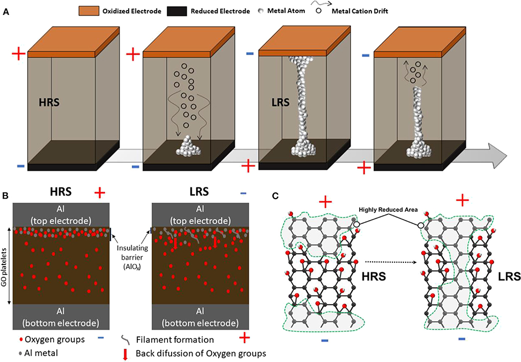
Figure 1. (A) Conceptual representation of the formation and annihilation of a metallic filament responsible for the resistive switching according to the metallic filamentary. (B) Model of the resistive switching in graphene oxide [adapted with permissions from Jeong et al. (2010)]. Copyright 2010 American Chemical Society. The as-fabricated device is in the HRS due to the insulating top interface layer formed by a redox reaction between Al and the GO film; The LRS state is induced by formation of filaments at the top interface layer due to oxygen ions diffusion by an external negative bias on the top electrode. (C) The GO surface is characterized by the combination of sp2 (green dashed areas) and sp3 domains. At a nanoscale level, the sp2 regions present high-conductivity but they are interrupted by low-conductivity sp3 domains rich in functional groups. When a current is flowing, the high resistivity of the sp3 domains creates local large gradients of electrostatic potential resulting in strong local electric fields. Joule heating of the high resistivity region triggers the drift of the oxygen containing groups (migration of functional groups), creating eventually a conductive filament.
When the ions reach the opposite electrode they gather together and the reduction reaction yields the growth of a metallic strand back to the ion reservoir electrode. When the filament is close enough to the anode, the resistance between the electrodes drops suddenly turning the HRS into the LRS of the device. This mechanism is typically characterized by very abrupt transitions between the current levels. Reversing the bias polarity, and therefore the electric field, causes a reverse diffusion of the metal ions that induce the rupture of the metallic filament.
The metallic filamentary model has been used to explain the resistance switching in thin GO memristors typically in stacked structures in-between to reactive metallic electrodes (Waser and Aono, 2007; He et al., 2009; Porro et al., 2015).
Contact Resistance Modification by Oxygen ION Drift
Jeong et al. pioneered a work (Jeong et al., 2010) where thin GO films were embedded in-between two Al electrodes showing potential for flexible non-volatile storage on a polyethersulfone substrate. Several experiments supported by X-ray diffraction, High Resolution Transmission Electron Microscopy, and also including the absence of an ohmic behavior, made the authors exclude the existence of a conducting filament in the bulk GO. In this case, the resistive switching is attributed to the formation/destruction of local filaments in the thin insulating layer at the interface between the top Al electrode and the bulk GO film. The authors hypothesized that those filaments were produced by the oxygen ion transfer between an insulating barrier (AlOx) at the interface of the top electrode in Figure 1B and the GO domain. Initially, the Al/GO electrode is expected to be amorphous and non-homogeneous due to the overlap of multiple GO platelets produced by the spin-casting deposition and redox reactions triggered at the interface. This region is expected to be rich in sp3 insulating domains constituting an insulating barrier that gives rise to the HRS. Under reverse bias polarity, local conductive filaments are grown by field-induced oxygen diffusion into the GO; thus the oxygen returns back to the bulk GO decreasing the insulating barrier and giving rise to the LRS. This model was further confirmed by replacing the electrode with an inert metal (Au) resulting in lack of resistive switching effect.
Several authors have postulated variations of this mechanism, i.e., oxygen ions drift leading to changes on the energy barrier at the interface GO-electrode, as the source of resistive switching in their GO experiments (Wang et al., 2012; Porro and Ricciardi, 2015), and despite the fact that in some cases the model described in Jeong et al. (2010) is not explicitly described (Kim et al., 2019), the resistive switching arguments provided are aligned with this approach.
Oxidation-Reduction Mechanisms in the Bulk Go
The third model explaining resistive switching in GO is connected to the drift of functional groups and its impact on the resulting different sp3 and sp2 domains on the bulk substrates (Khurana et al., 2013). This is particularly relevant to describe memristance in planar structures or to explain different set, and reset speeds. In this way, resistive switching is connected to a reversible filamentary phenomenon (Wei et al., 2012) in which the conductive path or paths are formed by turning insulating sp3 domains into conducting sp2 bonds (oxygen vacancies) based on the detachment of oxygen containing-groups under the action of an electric field, especially in those regions of low conductivity (Qi et al., 2018). This theory finds grounds in different first principles numerical simulation studies that demonstrate the formation of domains of highly functionalized Carbon interrupted by low oxidized domains (Kim et al., 2012; Zhou and Bongiorno, 2013); the stoichiometry of those domains is prone to be modified due to the low migration barrier of oxygen in GO (Dai et al., 2013; Zhou and Bongiorno, 2013). Figure 1C illustrates this process of resistive switching. The non-uniformity in the number and location of the functional groups of the partially reduced graphene oxide is responsible for the creation of regions of different conductance (or conductive domains). The sp2 regions present high-conductivity but they are interrupted by low-conductivity sp3 domains at a nanoscale level. When a current is flowing, the high resistivity of the sp3 domains create large gradients of electrostatic potential at a local level resulting in strong local electric fields. In this way, and assisted by the action of Joule heating in the switching material, there is a drift of oxygen containing groups that generate changes on the reduction level and therefore on the conductance. A recent experimental work (Romero et al., 2019) further supports this approach relating the memristance of GO with a bulk phenomenon involving the drift of oxygen ions and oxygen-containing groups inducing local changes in the stoichiometry level of the GO. The authors fabricated macroscopic size (~mm) laser-reduced graphene oxide based memristors concluding that due to the considerable distance between the electrodes and to the fact that under different contact approaches (including also organic electrodes) the resistive switching was present, it was necessary to rule out the creation of metallic filaments or the participation of the contacts in the process. Despite this model may be only appropriate for partially reduced GO, this work commits memristance in GO to the creation of a percolation path of highly reduced GO by the energy accumulated in the device. This theory agrees with the prospective estimation of the energy scale of the phenomenon given in Romero et al. (2019), and it is also supported by Times series Statistical Analysis (Rodriguez et al., 2019): the results thrown from the analysis of successive set and reset processes show that the autocorrelation and partial autocorrelation levels match those typically found in resistive switching due to a well-defined conductive path between the electrodes that it is interrupted at a Quantum Point Contact (Roldan et al., 2018).
Conclusion
The future of memristive devices relies on the development of adequate technologies able to outperform and provide additional value over the existing CMOS mainstream line. Among a plethora of material alternatives, GO based memristors have been pointed by many recent publications as one of the more interesting contenders due to promising switching properties, ultrathin thickness, easy processing approaches and intrinsic structural flexibility. However, there is still a long way to go to become a competitive technology, starting with an in-depth understanding and analytical description of the physical origins of its resistive switching features. There are three main sources of memristance acknowledged in the bibliography: first, considering the formation of a metallic filament due to the electrodes; second, attributing it to the change in the contact resistance, due to oxygen ions diffusion, as the main cause of the resistance changes; and finally, the third model, considering the evolution of the bulk GO conductance due to functional groups migration and the formation of a conductive path (formation of sp2 conductive domains). Those models share in common that the existence of functional groups in GO is responsible for the resistive switching. However, the ultimate impact of these functional groups on the physics and chemistry of the process is different in each case: metallic filament formation/destruction in the first model, contact resistance variation in the second, and formation of sp2 conductive paths according to the third model. The existing investigations have not excluded, or considered, the possibility of a combination of the former mechanisms as the source of memristance. In particular, the combination of a metallic filamentary mechanism in conjunction with the contact resistance modification is certainly a possibility whenever metallic electrodes are present. However, the case of an oxidation-reduction in the bulk is rather different, since, as demonstrated experimentally, resistive switching is present in the absence of metallic electrodes. Nevertheless, this model can be considered as another form of filamentary mechanisms, where the filament, in this case, is of an organic nature. For the time being, it is unclear though which one is the predominant mechanism causing the memristance in GO, but rather the experiments show that the particular device configuration (size of the active material, electrodes, and reduction level) determines the ultimate cause for the resistive switching.
Author Contributions
All authors listed have made a substantial, direct and intellectual contribution to the work, and approved it for publication.
Funding
This work has been supported by the Spanish Ministry of Science, Innovation and Universities/FEDER-EU through the project TEC2017-89955P and the pre-doctoral grants FPU16/01451, FPU16/04043, the Junta de Andalucía/FEDER-EU through the project B-RNM-375-UGR18 and the JSPS KAKENHI through grant number JP18k04275.
Conflict of Interest
The authors declare that the research was conducted in the absence of any commercial or financial relationships that could be construed as a potential conflict of interest.
References
Chua, L. (1971). Memristor-the missing circuit element. IEEE Trans. Circuit Theory 18, 507–519. doi: 10.1109/TCT.1971.1083337
Coroş, M., Pogăcean, F., Măgeruşan, L., Socaci, C., and Pruneanu, S. (2019). A brief overview on synthesis and applications of graphene and graphene-based nanomaterials. Front. Mater. Sci. 13, 23–32. doi: 10.1007/s11706-019-0452-5
Dai, Y., Ni, S., Li, Z., and Yang, J. (2013). Diffusion and desorption of oxygen atoms on graphene. J. Phys. Conden. Matter 25:405301. doi: 10.1088/0953-8984/25/40/405301
Dreyer, D. R., Park, S., Bielawski, C. W., and Ruoff, R. S. (2010). The chemistry of graphene oxide. Chem. Soc. Rev. 39, 228–240. doi: 10.1039/b917103g
He, C. L., Zhuge, F., Zhou, X. F., Li, M., Zhou, G. C., Liu, Y. W., et al. (2009). Nonvolatile resistive switching in graphene oxide thin films. Appl. Phys. Lett. 95:232101. doi: 10.1063/1.3271177
Hong, S. K., Kim, J. E., Kim, S. O., Choi, S. Y., and Cho, B. J. (2010). Flexible resistive switching memory device based on graphene oxide. IEEE Electr. Devices Lett. 31, 1005–1007. doi: 10.1109/LED.2010.2053695
Hui, F., Grustan-Gutierrez, E., Long, S., Liu, Q., Ott, A. K., Ferrari, A. C., et al. (2017). Graphene and related materials for resistive random access memories. Adv. Electron. Mater. 3:1600195. doi: 10.1002/aelm.201600195
Jeong, H. Y., Kim, J. Y., Kim, J. W., Hwang, J. O., Kim, J.-E., Lee, J. Y., et al. (2010). Graphene oxide thin films for flexible nonvolatile memory applications. Nano Lett. 10, 4381–4386. doi: 10.1021/nl101902k
Jo, S. H., Chang, T., Ebong, I., Bhadviya, B. B., Mazumder, P., and Lu, W. (2010). Nanoscale memristor device as synapse in neuromorphic systems. Nano Lett. 10, 1297–1301. doi: 10.1021/nl904092h
Khurana, G., Misra, P., and Katiyar, R. S. (2013). Forming free resistive switching in graphene oxide thin film for thermally stable nonvolatile memory applications. J. Appl. Phys. 114:124508. doi: 10.1063/1.4823734
Kim, S., Zhou, S., Hu, Y., Acik, M., Chabal, Y. J., Berger, C., et al. (2012). Room-temperature metastability of multilayer graphene oxide films. Nat. Mater. 11, 544–549. doi: 10.1038/nmat3316
Kim, T., Kim, D.-K., Kim, J., and Pak, J. J. (2019). Resistive switching behaviour of multi-stacked PVA/graphene oxide + PVA composite/PVA insulating layer-based RRAM devices. Semiconduc. Sci. Technol. 34:065006. doi: 10.1088/1361-6641/ab1403
Lanza, M., Wong, H.-S. P., Pop, E., Ielmini, D., Strukov, D., Regan, B. C., et al. (2018). Recommended methods to study resistive switching devices. Adv. Electron. Mater. 5:1800143. doi: 10.1002/aelm.201800143
Lee, M. J., Park, Y., Suh, D. S., Lee, E. H., Seo, S., Kim, D. C., et al. (2007). Two series oxide resistors applicable to high speed and high density nonvolatile memory. Adv. Mater. 19, 3919–3923. doi: 10.1002/adma.200700251
Li, Y., Zhang, M., Long, S., Teng, J., Liu, Q., Lv, H., et al. (2017). Investigation on the conductive filament growth dynamics in resistive switching memory via a universal monte carlo simulator. Scient. Rep. 7:11204. doi: 10.1038/s41598-017-11165-5
Mohammad, B., Jaoude, M. A., Kumar, V., Al Homouz, D. M., Nahla, H. A., Al-Qutayri, M., et al. (2016). State of the art of metal oxide memristor devices. Nanotechnol. Rev. 5, 311–329. doi: 10.1515/ntrev-2015-0029
Porro, S., Accornero, E., Pirri, C. F., and Ricciardi, C. (2015). Memristive devices based on graphene oxide. Carbon 85, 383–396. doi: 10.1016/j.carbon.2015.01.011
Porro, S., and Ricciardi, C. (2015). Memristive behaviour in inkjet printed graphene oxide thin layers. RSC Adv. 5, 68565–68570. doi: 10.1039/C5RA11058K
Pradhan, S. K., Xiao, B., Mishra, S., Killam, A., and Pradhan, A. K. (2016). Resistive switching behavior of reduced graphene oxide memory cells for low power nonvolatile device application. Scient. Rep. 6:26763. doi: 10.1038/srep26763
Qi, M., Bai, L., Xu, H., Wang, Z., Kang, Z., Zhao, X., et al. (2018). Oxidized carbon quantum dot–graphene oxide nanocomposites for improving data retention of resistive switching memory. J. Mater. Chem. C 6, 2026–2033. doi: 10.1039/C7TC04829G
Rodriguez, N., Maldonado, D., Romero, F. J., Alonso, F. J., Aguilera, A. M., Godoy, A., et al. (2019). Resistive switching and charge transport in laser-fabricated graphene oxide memristors: a times series and quantum point contact modeling approach. Laser-fabricated reduced graphene oxide memristors. Materials 12:3734. doi: 10.3390/ma12223734
Roldan, J. B., Miranda, E., Gonzalez-Cordero, G., Garcia-Fernandez, P., Romero-Zaliz, R., Gonzalez-Rodelas, P., et al. (2018). Multivariate analysis and extraction of parameters in resistive RAMs using the Quantum Point Contact model. J. Appl. Phys. 2018:014501. doi: 10.1063/1.5006995
Romero, F. J., Toral-Lopez, A., Ohata, A., Morales, D. P., Ruiz, F. G., Godoy, A., et al. (2019). Laser-fabricated reduced graphene oxide memristors. Nanomaterials 9:897. doi: 10.3390/nano9060897
Sparvoli, M., Gazziro, M. A., Marma, J. S., and Zucchi, G. (2019). “Memristor device fabricated from doped graphene oxide,” in 2019 IEEE 10th Latin American Symposium on Circuits & Systems (LASCAS) (Armenia). doi: 10.3390/nano9040518
Van den Hurk, J., Menzel, S., Waser, R., and Valov, I. (2015). Processes and limitations during filament formation and dissolution in GeSx-based ReRAM memory cells. J. Phys. Chem. C 119, 18678–18685. doi: 10.1021/acs.jpcc.5b03622
Wang, C., Wu, H., Gao, B., Zhang, T., Yang, Y., and Qian, H. (2018). Conduction mechanisms, dynamics and stability in ReRAMs. Microelectr. Eng. 187–188, 121–133. doi: 10.1016/j.mee.2017.11.003
Wang, L. H., Yang, W., Sun, Q. Q., Zhou, P., Lu, H. L., Ding, S. J., et al. (2012). The mechanism of the asymmetric SET and RESET speed of graphene oxide based flexible resistive switching memories. Appl. Phys. Lett. 100:063509. doi: 10.1063/1.3681366
Wang, Z., Joshi, S., Savel'ev, S. E., Jiang, H., Midya, R., Lin, P., et al. (2016). Memristors with diffusive dynamics as synaptic emulators for neuromorphic computing. Nat. Mater. 101–108. doi: 10.1038/nmat4756
Waser, R., and Aono, M. (2007). Nanoionics-based resistive switching memories. Nat. Mater. 6, 833–840. doi: 10.1038/nmat2023
Wei, H. Q., Zhou, P., Sun, Q. Q., Wang, L. H., Geng, Y., Zhang, D. W., et al. (2012). “The nano-scale resistive memory effect of graphene oxide,” in 2012 IEEE Nanotechnology Materials and Devices Conference (NMDC2012) (Waikiki Beach, HI). doi: 10.1109/NMDC.2012.6527574
Yu, H., Zhang, B., Bulin, C., Li, R., and Xing, R. (2016). High-efficient synthesis of graphene oxide based on improved hummers method. Scient. Rep. 6:36143. doi: 10.1038/srep36143
Yu, S. (2017). Neuro-inspired Computing Using Resistive Synaptic Devices. Cham: Springer International Publishing. doi: 10.1007/978-3-319-54313-0
Yu, S., Wu, Y., Jeyasingh, R., Kuzum, D., and Wong, H. S. P. (2011). An electronic synapse device based on metal oxide resistive switching memory for neuromorphic computation. IEEE Trans. Electr. Devices 58, 2729–2737. doi: 10.1109/TED.2011.2147791
Zhou, S., and Bongiorno, A. (2013). Origin of the chemical and kinetic stability of graphene oxide. Scient. Rep. 3:2484. doi: 10.1038/srep02484
Zhou, Z., Yan, X., Zhao, J., Chao, L., Ren, D., Lu, N., et al. (2019). Synapse behavior characterization and physics mechanism of a TiN/SiOx/p-Si tunneling memristor device. J. Mater. Chem. C 7, 1561–1567. doi: 10.1039/C8TC04903C
Zhuge, F., Dai, W., He, C. L., Wang, A. Y., Liu, Y. W., Li, M., et al. (2010). Nonvolatile resistive switching memory based on amorphous carbon. Appl. Phys. Lett. 96:163505. doi: 10.1063/1.3406121
Keywords: graphene, graphene oxide, memristor, ReRAM, laser-reduction
Citation: Romero FJ, Toral A, Medina-Rull A, Moraila-Martinez CL, Morales DP, Ohata A, Godoy A, Ruiz FG and Rodriguez N (2020) Resistive Switching in Graphene Oxide. Front. Mater. 7:17. doi: 10.3389/fmats.2020.00017
Received: 24 September 2019; Accepted: 14 January 2020;
Published: 31 January 2020.
Edited by:
Zoltán Kónya, University of Szeged, HungaryReviewed by:
Tamas Szabo, University of Szeged, HungaryVyacheslav Demin, Kurchatov Institute, Russia
Copyright © 2020 Romero, Toral, Medina-Rull, Moraila-Martinez, Morales, Ohata, Godoy, Ruiz and Rodriguez. This is an open-access article distributed under the terms of the Creative Commons Attribution License (CC BY). The use, distribution or reproduction in other forums is permitted, provided the original author(s) and the copyright owner(s) are credited and that the original publication in this journal is cited, in accordance with accepted academic practice. No use, distribution or reproduction is permitted which does not comply with these terms.
*Correspondence: Noel Rodriguez, bm9lbEB1Z3IuZXM=