 Yann Danlée
 Francisco Mederos-Henry
 Sophie Hermans
 Christian Bailly
 Isabelle Huynen
- 1BSMA Division, Institute IMCN, Université Catholique de Louvain (UCLouvain), Louvain-la-Neuve, Belgium
- 2ELEN Division, Institute ICTEAM, UCLouvain, Louvain-la-Neuve, Belgium
- 3MOST Division, Institute IMCN, UCLouvain, Louvain-la-Neuve, Belgium
Because electromagnetic (EM) pollution of the environment is becoming such a pervasive issue, highly efficient solutions for EM protection are being keenly sought for. Our approach provides new avenues to simple, compact, and efficient broadband microwave absorbers designed to cancel EM interferences in the microwave range. The paper demonstrates the potential of a clever organization of nanoscale inclusions (carbon nanotubes, graphene, magnetic metallic nanowires or nanoparticles) in polymer matrices for controlling the propagation of microwaves over a wide range of wavelengths (10−3-10−1 m), focusing on broadband absorption. Controlled architectures of polymer composites loaded with various nanofillers, and in particular layered stacks of composite films enable optimization of the absorption bandwidth while preserving the compactness of the structure. First, various carbon-based and metallic nanofillers are synthesized. Next, nanofillers are dispersed in a polymer matrix thanks to melt polymer processing and dispersion techniques. The absorption characteristics of resulting thin composite slabs are first characterized. Various combinations of superposed slabs are then investigated and modeled in order to optimize the absorption of the resulting multilayers. As innovative approach, the performances of the investigated structures are finally compared with the help of a new figure of merit combining the maximum absorption and its bandwidth.
Introduction
As stated in Danlée et al. (in press), electromagnetic (EM) waves are omnipresent in the present domestic and working place environments. The rising number of electronic devices and the trend toward increasing wideband wireless communication is becoming an issue. Indeed, it generates electromagnetic interference (EMI) between devices or their subcomponents. Moreover, some people are developing electromagnetic hypersensitivity (EHS) disorder. Therefore, EMI must be reduced to avoid dangerous consequences for health, safety or security, especially in the case of some sensitive applications (Violette and Violette, 1987). EMI broadband shielding is usually achieved by using electromagnetic reflectors, such as metal foils or coatings, acting as Faraday cages (Leland, 1992). However, these methods are becoming less satisfactory because the EM signal is reflected in another direction and can still interfere with nearby (sub)devices without significant loss. This is especially non-suitable given the above-mentioned health concern and technological intensification. These considerations have given renewed popularity to EM absorbers. In this case, the goal is to truly eliminate the EM signal, especially in areas where it is unwanted.
The effective EM absorption of a material requires balancing its complex permittivity and permeability (Danlée et al., 2014). Indeed, transmission and reflection must both be minimized, which is normally contradictory. The EM transmission can be defined as:
where d is the thickness of material, ω is the pulsation and c is the speed of light in vacuum. Low transmission is favored by high values of the imaginary part of permittivity εr and permeability μr. In the composite materials considered in this paper, the imaginary part of εr is associated to conduction losses induced by conducting charges loading the absorber. The real part to dielectric losses is induced by the polymer hosting matrix, namely by dielectric relaxation and interfacial polarization. In turn, the imaginary par of μr is associated to hysteresis and ferromagnetic resonance losses present in magnetic inclusions. Both contribute to absorption responsible for low transmission. Moreover, imaginary parts of εr and μr are proportional to concentrations in conductive and magnetic inclusions, respectively, so that concentration in nanocharges is able to tailor the level of absorption.
Reflection is reduced when the complex values of the two are close to each other as this minimizes the reflection coefficient at material/air interface as defined by Kong (2000):
The corresponding demands are impossible to combine in a simple material but can be reconciled in hybrid structures, including polymer-based nanocomposites containing conductive as well as ferromagnetic fillers (Chung, 2001; Gao et al., 2008). Highly conductive carbon nanotubes (CNTs) and metallic nanowires (NWs) are natural choices for the conductive filler (Saib et al., 2005). Multiwall CNTs have a low percolation threshold because of their high aspect ratio and easy dispersibility in selected polymers. They tend to form loose conductive networks inside the polymer matrix (Thomassin et al., 2007). The matrix, in contrast, has low permittivity and therefore EM waves can penetrate deeply in the absorbing structure allowing the conducting network to dissipate the energy by two major mechanisms, i.e., complex resistive-capacitive coupling and multiple internal reflections (Pötschke et al., 2002). However, CNTs are diamagnetic and hence can only absorb the electric field of the EM wave. On the other hand, conducting ferromagnetic inclusions such as Ni nanowires can also dissipate the magnetic field. Hence it is attractive to combine electric conductivity and magnetism in the absorber because of the expected synergy. This has recently been exploited in new types of high-performance absorbers, e.g., magnetic nanowires in a polymer matrix (Gao et al., 2008), magnetic nanoparticles (MNPs) attached to carbon nanostructures (Mederos-Henry et al., 2016) or even ferromagnetic particles trapped inside CNTs (Gui et al., 2009). However, Nam et al. (2009) and Raj et al. (2014) have shown that only magnetic nanowires provide high enough permeability to yield a significant absorption enhancement.
Beside controlling the material properties at the nano- and microscale it is possible to exploit the architecture of the absorber at a “meso” scale, from the 100 to the 1000 micrometers range. A conductivity and/or magnetic permeability gradient can be optimized to match impedance at the incoming wave front (Bhattacharjee et al., 2017) but favor dissipation in the depth of the structure. In this way, the EM energy can be “trapped” between the internal lossy layers through multiple reflections while keeping back reflection low (Danlée et al., 2020, 2014). This results in higher absorption because the reflected power is reduced.
The present contribution describes various original architectures of microwave absorbers developed in our research team at UCLouvain, based on combinations of magnetic and conductive nanostructures. Considered nanostructures are carbon nanotubes (CNTs), reduced graphene oxide (rGO) nanoplatelets, magnetic nanostructures (MNSs) and nanowires (NWs). Special attention is devoted to broadband performance achieved with multilayered structures consisting of thin composite polymer slabs. The performances of the investigated structures are finally compared with the help of a new figure of merit combining the maximum absorption value and its bandwidth.
Section Materials and Methods describes the methodology and simulation/experimental tools used in this work, while section Results and Discussion presents the results and proposes a new figure of merit to rank the various structures, and section Conclusion draws conclusions about the work. Five different architectures are presented: a polymer-CNT gradient absorber, a CNT-ink based absorber, a magnetic nanowire film and its combination with CNT, and a gradient absorber based on MNPs decorating rGO.
Materials and Methods
Strategy
The hierarchical methodology driving our approach is illustrated in Figure 1. Conductive carbonaceous nano-supports combined with metallic magnetic nanostructures are included into polymer-hosting thin films that are stacked together to form multilayered gradient structures allowing broadband absorption.
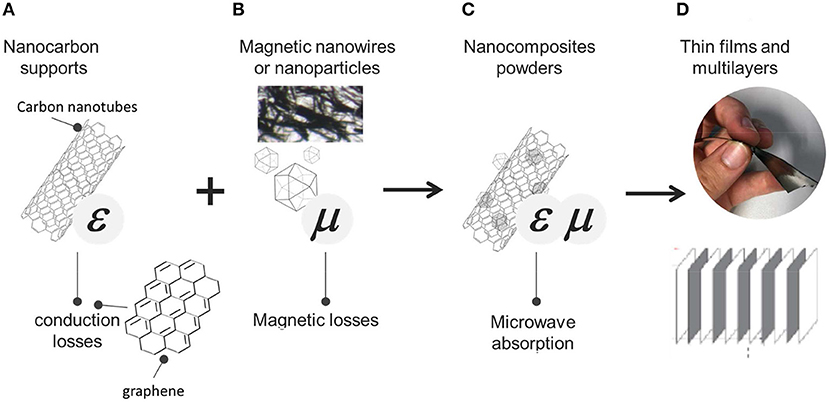
Figure 1. Illustration of the approach: conductive inclusions (A), responsible for dielectric constant and conductivity, and magnetic nanostructures (B) are combined to induce microwave absorption (C) and are dispersed in polymer matrix, to form thin films that are stacked to form multilayers (D). Considered polymer is polycarbonate well known for its stiffness allowing flexibility.
The polymer considered in this paper is polycarbonate (Makrolon OD 2015 and Lexan™ grades); it is well known for its excellent mechanical properties, i.e., stiffness, strength and toughness, yielding a flexural modulus roughly equal to 2,300 MPa.
Hierarchical Organization at Millimeter Scale
Stacking multiple layers of films allows creating a periodic or gradient structuration of isotropic or pre-oriented nanocomposites (Figure 1D), alternating insulating polymer and conductive nanocomposite films. Experiments confirm (Danlée et al., 2020) that a gradient arrangement of conductive layers favors the penetration and progressive absorption of EM waves through a nanocomposite (Figure 3A). Once the physical parameters of each layer are known, the scattering parameters (S-parameters) are simulated using a simple method based on chain matrix conversion (Saib and Huynen, 2005), and the absorption is derived from Equation (4). The simulation shown in Danlée et al. (in press) Figure 2B shows that a periodic stack alternating insulating polycarbonate layers and layers having graded increasing conductivity induces lower reflection and higher absorption than when using layers having uniform equivalent conductivity. This demonstrates the superior performance of a generic gradient structure compared to a straightforward periodic one with the same overall loading of conductive filler. The concept is applied in section CNT-Ink Absorber for polymer gradient absorber.
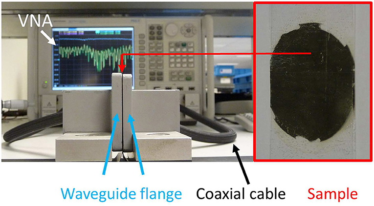
Figure 2. Illustration of the measurement configuration used for our nanocomposites. Each sample is inserted between the two waveguide flanges that are connected to the Vector Network Analyzer (VNA) trough coaxial cables.
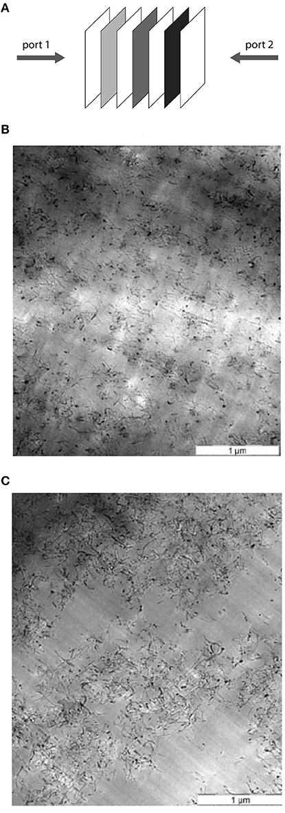
Figure 3. Multilayer gradient topology (A) and TEM images of PC-CNT melt-blended composites with 1 wt.% CNT concentration (B) or 7.5 wt.% CNT concentration (C).
Synthesis of MNPs (Magnetic Nanoparticles)@NCS(Nanocarbon Supports) Nanocomposites
Multiwalled Carbon Nanotubes (MWCNTs) were purchased by Nanocyl SA, Belgium. The preparation of FeNi, CoNi and FeCoNi alloyed nanoparticles supported on graphene oxide (GO) was performed using a Pechini-type sol-gel method fully described in Mederos-Henry et al. (2019a).
Synthesis of Nanowires
Gold nanowires (Au-NWs) as well as nickel nanowires (Ni-NWs) were produced and embedded into polymer nanocomposites. All nanowires were synthesized using an electrodeposition process. The process involves the reduction of metal ions from an electrolyte solution in the pores of a nanoporous alumina template in order to form an array of nanowires (Danlée et al., in press). This process gives metallic nanowires of the wanted element or alloy with a well-defined aspect ratio. The nanowires are formed in the pores of a UniKera Standard alumina membrane (Al2O3) from Synkera (nowadays IDT). This template has a pore areal density up to 35%, while the diameter of the pores is 150 nm and the thickness of the membrane is 100 μm. Hence, the aspect ratio of the NWs is about 667 (assuming a perfect filling of the pores). The alumina template is then dissolved and the resulting solution is removed by filtration with the help of a polycarbonate ipPORE™ Track Etched Membrane from it4ip. This 25 μm-thick porous film with a pore density of 5.108 cm−2 and a pore diameter of 200 nm is used as a filter to collect NWs on its surface. The entangled NWs are then sandwiched between two 55 μm-thick Lexan polycarbonate (PC) films (see Danlée et al., in press for process details).
Composite Polymer Processing
The process was fully described in Mederos-Henry et al. (2020) and is recalled here for sake of completeness. The polymer matrix of all composites is polycarbonate (PC) Makrolon OD2015 resin pellets purchased from Bayer as detailed in Jaiswar et al. (2019). Before processing, PC pellets were dried for 24 h at 80°C in vacuo to remove any water residues, which can degrade the polymer and induce unwanted effects on the electrical and mechanical properties. The polymer-nanofiller dry-blends were compounded in a DSM Xplore microcompounder at 260°C and 150 rpm for 15 min after a feeding time of 1–2 min. The MWCNTs were dispersed (Mesfin et al., 2015; Jaiswar et al., 2019) in low viscosity PC designed for the molding of CDs and DVDs storage media, at various weight concentrations and ratios. The low viscosity of the matrix and high torque capability of the machine allowed for a lower processing temperature than usual for PC while achieving excellent dispersion of the nanofillers (Mesfin et al., 2015; Jaiswar et al., 2019). Afterwards, the extrudates were hot pressed for 2 min at 260°C and 10 MPa using a hydraulic press, into thin flat sheets and finally annealed at 150°C for 5 h and cold pressed before characterization (Pötschke et al., 2004).
Characterization Tools
TEM imagery was performed on nanocomposites and multilayers with the help of a Zeiss Leo 922 working at 200 kV and equipped with an Omega-A filter. The specimens were cut with the help of a Reichert Microtome. Ultrathin sections of approximately 70–100 nm in thickness were cut using a cryodiamond knife (Diatome, Switzerland) and collected on 400 mesh copper grids. The whole procedure is very similar to that described in Emplit et al. (2017).
The microwave characterization procedure standardly used in our group is described in Mederos-Henry et al. (2020) and recalled here. A Vector Network Analyzer (VNA) was used to measure the transmission of a microwave signal through the materials and devices under scope, noted S21, as well as the reflection at their input, noted S11. Three VNAs were used during the project: Wiltron 360 and 37397C from Anritsu, and N5247A PNA-X 67 from Agilent/Keysight. They operate in the 40 kHz−65 GHz frequency range. The measurement of thin film absorbers developed during the work is fully described in Quiévy et al. (2012). Each sample is inserted between the two waveguide flanges connected to the VNA through coaxial cables as illustrated in Figure 2. Using this configuration, the reflection at input of the absorber and absorption through it are obtained from the reflection S11 and transmission S21 coefficients measured by the VNA as:
Measurements of saturation magnetization for magnetic nanoparticles were obtained with a MPMS-XL5 SQUID magnetometer (Quantum Design, U.S.A.).
Results and Discussion
Polymer Gradient Absorber
The multilayer CNT-PC melt-blended composite presented in this section is based on the work in Danlée et al. (2014) and consists of 3 composite layers having a conductivity gradually increasing from 50, 90 to 100 S/m, with a corresponding loading of 2–5 and finally 7.5 wt.% of CNTs. Each composite layer has a thickness of about 150 μm, and is separated by a pure PC sheet 165 μm-thick (Figure 3A). Illustrative TEM images are provided in Figures 3B,C for 1 and 7.5 wt.% CNT layers, respectively.
This novel multilayer arrangement of polymer nanocomposites is able to either effectively absorb microwave signals over a wide frequency range or selectively reflect desired wavelengths. The stacked multilayers are easy to make, modular, and open up new possibilities in the area of microwave management (broadband shielding by absorption or frequency-selective filtering, also called bandgap control).
Figure 4A clearly shows that the level of absorption depends on the direction of measurement (from port 1 to port 2, or from port 2 to port 1). Absorption is favored from port 1 to port 2, which is correlated to the increasing gradient of conductivity inducing a lower reflection coefficient at port 1 (Figure 4B). The resulting level of absorption rises up to 70% for a total thickness of the sample equal to 0.39 mm. A residual mismatch of the waveguide flanges used for the measurements explains the oscillations observed on the curves, as detailed in Mederos-Henry et al. (2019b) and briefly recalled here. Although explanations were provided for powder nanocomposites samples, it also applies to samples presented in this paper. Indeed, oscillation ripple observed in the experimental curves is due to the mismatch between the reference impedance of the VNA measuring equipment and the impedance of the device under test, here the nanocomposite sample (Dunsmore, 2012). The value of the latter impedance depends on the dielectric constant of the sample under scope, a priori unknown, so that oscillation ripple on S parameters cannot be avoided, and affects absorption as well by virtue of Equation (4). Despite this ripple, the trend behavior of absorption can be clearly retrieved from its averaged value, as we did verify by simulation.
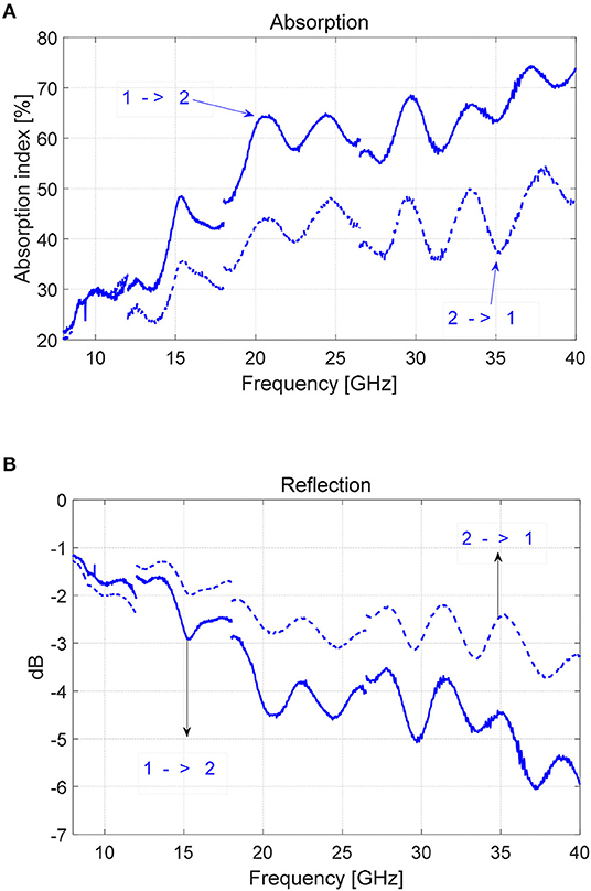
Figure 4. Absorption (A) and reflection (B) measurements of CNT-polymer gradient composite.
CNT-Ink Absorber
A water-based suspension of CNT called AquaCyl™ AQ0101 was provided by the NanoCyl company. It contains 98% of pure water, 1% of multi-walled CNT and 1% of surfactant. The suspension is applied just as a conventional ink on surface-plasma-treated polycarbonate films. In this way, we obtain an alternative for forming a dielectric-conductor layer stacking. The dielectric is still a polycarbonate film, but the conductive layer now consists of an ultra-thin coating of entangled carbon nanotubes sandwiched between two PC films, as detailed in Danlée et al. (2014) and shown in TEM Figure 5A. Again it is observed in Figures 5B,C that the stack of CNT ink-PC sandwich layers having increasing concentration of CNTs, hence of conductivity, allows to maximize absorption (Figure 5C) and minimize reflection (Figure 5B), when the propagation of signal occurs in the direction of increasing gradient concentration, i.e., from port 1 to port 2 as shown in Figure 3A.
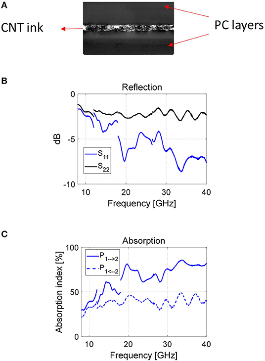
Figure 5. TEM image of sandwich PC-CNT ink (A), adapted from Danlée et al. (2014) measured reflection coefficient of a stack of sandwich PC-CNT ink layers having increasing concentration (B) corresponding absorption measurement (C).
The CNT-ink based gradient is advantageous over blended composites since its overall thickness is only 375 μm, while the structure previously shown in section Polymer Gradient Absorber is about 1 mm thick.
Nanowires-Based Absorber
In order to investigate the benefit of magnetic inclusions over conductive inclusions, a comparative study of the absorption performances of absorbers using gold conductive nanowires or nickel magnetic nanowires has been conducted. The synthesis of nickel nanowires is fully described in Danlée et al. (in press) and in section Synthesis of Nanowires. The synthesis of gold NW follows the same method. An electrodeposition process is used to grow NW in a nanoporous polycarbonate template, which is subsequently dissolved. In both cases, the absorber configuration exploits the residues of the synthesis process. Indeed nanowires (NW) resulting from the dissolution of the alumina template are collected on a filtering polycarbonate membrane, with various weight concentrations. The filter covered with NWs is inserted between two 55 μm-thick Lexan™ polycarbonate films. The resulting sandwich is hot pressed at 210°C and 10 T for 30 s. This very simple process provides a thin conductive and magnetic film. Figure 6 (top) illustrates the formation of the NW-polymer bilayer: the filtering membrane acts as a support for the NW, the whole structure forming a conducting layer responsible for microwave absorption.
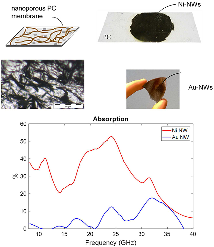
Figure 6. Topology of metallic nanowires absorber; the NWs are collected on the filtering membrane in order to form the absorbing structure that is then inserted between two 55 μm-thick Lexan™ polycarbonate films, and comparison between absorption induced by Ni-and Au-nanowires based-sandwich structures, respectively, obtained from Equation (4).
Figure 6 (bottom) compares the absorption performances obtained for PC/Ni and PC/Au sandwiched layers having similar 1 wt.% concentration. It is evident that the presence of Ni-NW enhances the absorption. This is explained by the fact that magnetic materials improve the matching of the input impedance with respect to air, by virtue of Equation (2). As a result, the reflection at the input interface of the absorber is reduced, favoring the penetration of the signal in the nanowires layer where it undergoes absorption due to both conductive and magnetic losses inside Ni-NW.
Magnetic NW/CNT Bilayer Absorber
Obviously, the various absorbing structures presented until now can be combined in various ways. For example, an absorbing structure combining magnetic nano-inclusions and conductive CNT inclusions can be formed through the stacking of the Ni-NW absorber presented in section Nanowires-Based Absorber having a thickness of 1.04 mm with a conductive absorber similar to that presented in section CNT-Ink Absorber, i.e., a CNT-ink sandwiched between 2 polycarbonate layers for a total thickness of 190 μm. Figure 7 shows the improvement of absorption resulting from the stacked combination. Indeed, the blue curve demonstrates a 20% absorption gain over composite absorbers containing only CNT or Ni-NW at frequencies above 26 GHz. As a result of this combination, the absorption is maintained roughly around 50% from 20 to 40 GHz. At low frequencies, the absorption is achieved through magnetic losses induced by nanowires, while at high frequencies the CNT ink layer induces sufficient losses so as to compensate the decrease of the absorption observed for the sole Ni-NWs. This promising result might certainly be improved by an adequate tuning of the composition and thicknesses of the considered layers.
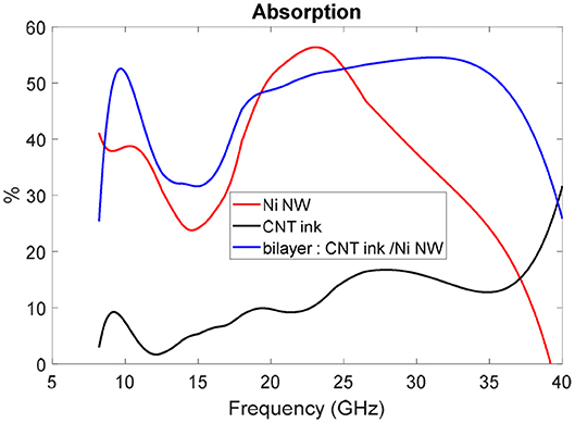
Figure 7. Combination of CNT-layer and Ni NW-layer for improved absorption. The Ni-NW/CNT bilayer is constructed and measured by stacking together a CNT layer and a Ni-NW layer similar to section Nanowires-Based Absorber.
Because of their flexibility and low thickness, the structures of sections CNT-Ink Absorber to Magnetic NW/CNT Bilayer Absorber can adapt to almost any shape and thus isolate devices from external and internal fields. The Ni-NW film absorbers are particularly suited for specific compact devices such as microchips, sensors, or medical probes.
Magnetic Gradient Absorber
Another idea for realizing broadband absorbers is to exploit a gradient created by magnetic nanoparticles with increasing saturation magnetization. Three kinds of alloyed magnetic nanoparticles (MNPs) are considered here: permalloy (NiFe), a cobalt-iron alloy (CoFe), and a trimetallic cobalt-iron-nickel (CoFeNi) alloy, each deposited on reduced graphene oxide (rGO). The synthesis of these particles uses a Pechini sol-gel method and is fully described in Mederos-Henry et al. (2019a). The corresponding saturation magnetization Ms of the MNPs is given in Table 1. TEM images of NiFe, CoFe and CoFeNi MNPs are shown as bottom line in Figure 8. They reveal that the Pecchini synthesis yields a uniform distribution of MNPs on rGO.
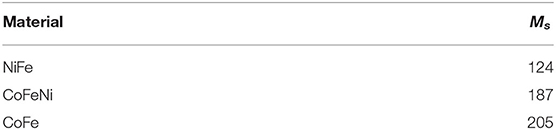
Table 1. Saturation magnetization values measured by SQUID for MNPs anchored on rGO.
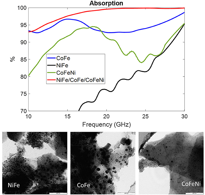
Figure 8. Absorption resulting from a gradient of the saturation magnetization values of magnetic nanoparticles. Bottom line shows TEM images for MNPs considered in this paper. Scale bar is 200 nm.
When the value of Ms increases, it means that magnetic losses associated to hysteresis and ferromagnetic resonance increase, which in turn is responsible for EM absorption increase. If a stack is composed of layers with increasing values of Ms, it is expected to induce an increase gradient of magnetic losses and hence of absorption. This is indeed observed in Figure 8. The measured absorption of monolayers made of NiFe, CoFeNi, and CoFe shows an increasing trend following their saturation magnetization values. More importantly, the multilayer formed by the stack NiFe/CoFeNi/CoFe, which behavior is predicted/calculated using the approach explained in section Hierarchical Organization at Millimeter Scale, allows to maximize the absorption up to nearly 100% from 15 up to 30 GHz.
Comparative Assessment of Performance: A Figure of Merit Proposal
This paper presents a wide variety of effective absorber structures in the microwave range, distinguished by architecture as well as composition. It is highly desirable to identify a figure of merit (FOM) allowing to compare their performances. The general definition of a “figure of merit” (FOM) is: a numerical quantity based on one or more characteristics of a system or device that represents a measure of efficiency or effectiveness.
Here the FOM is defined such as allowing the comparison of the performance of the various absorber structures. Since we are primarily interested in broadband absorption at the highest frequencies, we propose the following formula combining the maximum absorption and the fractional bandwidth:
where Amax is the maximal level of absorption in %, BW is the frequency range in which this absorption occurs (in GHz), while fo (in GHz) is the center frequency of the absorption bandwidth. Table 2 provides the FOM for the 5 topologies of absorbers proposed in this work, deduced from the absorption curves presented in sections Polymer Gradient Absorber to Magnetic Gradient Absorber.
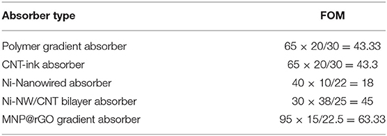
Table 2. Comparison of figure of merit (FOM) defined by Equation (5).
The provisional conclusion is that the MNPs@rGO multilayered gradient absorber and the Ni-CNT bilayer absorber show the highest FOM, but this could be confirmed in the future by additional experimental investigations, which are beyond the scope of this paper.
Conclusion
Fine-tuned combinations of conductive and/or ferromagnetic nanofillers (CNTs, NWs, MNPs on NCSs…) within a polycarbonate dielectric film have clearly proven their efficiency for broadband microwave absorption. The selected nanofillers either yield suitable shields for covering large surfaces or effective ones for miniaturized devices requiring very high absorption/thickness ratio. A smart hierarchical architecture of the absorbers combining nanoscale filler dispersion and mesoscale stacking of films in gradient of filler concentration is key for optimized performance, with the additional benefit of easy assembly. The multilayers are thin compared to the wavelength and benefit from the classical advantages of polymers: easy processability, mechanical resistance, flexibility and conformability. The combination of thinness and easiness of elaboration is a strong practical benefit. A new FOM has been defined in order to rank the five absorber systems presented in the paper, based on their absorption level and frequency range of absorption. The approach can be useful for further optimizations by experts in the field of commercial absorbers solutions.
Data Availability Statement
The raw data supporting the conclusions of this article will be made available by the authors, without undue reservation.
Author Contributions
YD and IH: Modeling and simulation. FM-H and YD: Experimental investigations. CB, SH, and IH: Supervision, funding acquisition, writing, and review and editing. All authors contributed to the article and approved the submitted version.
Funding
The authors are grateful to the National Fund for Scientific Research (FRS-FNRS) Belgium, for funding this research. This work is also supported by the Walloon region, and by the Communauté Française de Belgique, through the project Nano4waves funded by its research program Actions de Recherche Concertées.
Conflict of Interest
The authors declare that the research was conducted in the absence of any commercial or financial relationships that could be construed as a potential conflict of interest.
Acknowledgments
Special thanks are due to Prof. Arnaud Delcorte and Prof. Jean-Pierre Raskin for fruitful discussions, to the researchers who contributed to the success of the Nano4waves project, and to the technical staff of UCLouvain technological platforms SUCH, MICA, Winfab and Welcome.
References
Bhattacharjee, Y., Arief, A., and Bose, I. (2017). Recent trends in multi-layered architectures towards screening electromagnetic radiation: challenges and perspectives. J. Mat. Chem. C, 5, 7390–7403. doi: 10.1039/C7TC02172K
Chung, D. (2001). Electromagnetic interference shielding effectiveness of carbon materials. Carbon 39, 279–285. doi: 10.1016/S0008-6223(00)00184-6
Danlée, Y., Bailly, C., and Huynen, I. (2014). Thin and flexible multilayer polymer composite structures for effective control of microwave electromagnetic absorption. Comp. Sci. Technol. 100, 182–188. doi: 10.1016/j.compscitech.2014.06.010
Danlée, Y., Bailly, C., Huynen, I., and Piraux, L. (in press). Flexible multilayer combining nickel nanowires polymer films for broadband microwave absorption. IEEE Trans. Electrom. Comp. doi: 10.1109/TEMC.2019.2943549
Danlée, Y., Huynen, I., and Bailly, C. (2020). Thin smart multilayer microwave absorber based on hybrid structure of polymer and carbon nanotubes. Appl. Phys. Lett. 100:213105. doi: 10.1063/1.4717993
Dunsmore, J. P. (2012). Handbook of Microwave Component Measurements: With Advanced VNA. Chichester: Wiley.
Emplit, A., Bailly, C., and Huynen, I. (2017). Polypropylene carbon nanotubes nanocomposites -combined influence of block copolymer compatibilizer and melt annealing on electrical properties. J. Nanomat. 11:878. doi: 10.1155/2017/9075878
Gao, B., Qiao, L., Wang, J., Liu, Q., Li, F., Feng, J., et al. (2008). Microwave absorption properties of the Ni nanowires composite. J. Phys. D 41:235005. doi: 10.1088/0022-3727/41/23/235005
Gui, G., Ye, W., Wei, J., Wang, K., Lu, R., Zhu, H., et al. (2009). Optimization of electromagnetic matching of Fe-filled carbon nanotubes/ferrite composites for microwave absorption. J. Phys. D 42:075002. doi: 10.1088/0022-3727/42/7/075002
Jaiswar, R., Bailly, C., Hermans, S., Raskin, J. P., and Huynen, I. (2019). Wideband microwave absorption in thin nanocomposite films induced by a concentration gradient of mixed carbonaceous nanostructures. J. Mater. Sci. Mater. Electron. 30, 19147–19153. doi: 10.1007/s10854-019-02271-3
Leland, L. H. (1992). Architectural Electromagnetic Shielding Handbook: A Design and Specification Guide. Hoboken, NJ: WILEY IEEE Press.
Mederos-Henry, F., Hermans, S., and Huynen, I. (2019b). Microwave characterization of metal-decorated carbon nanopowders using a single transmission line. J. Nanomat. 2019:3280461. doi: 10.1155/2019/3280461
Mederos-Henry, F., Mahin, J., Pichon, B., Durtu, M., Garcia, Y., Delcorte, A., et al. (2019a). Highly efficient wideband microwave absorbers based on zero-valent Fe@γ-Fe2O3 and Fe/Co/Ni carbon-protected alloy nanoparticles supported on reduced graphene oxide. Nanomaterials 9:1196. doi: 10.3390/nano9091196
Mederos-Henry, F., Mesfin, H., Danlée, Y., Jaiswar, R., Delcorte, A., Bailly, C., et al. (2020). Smart nanocomposites for nanosecond signal control: the Nano4waves approach. Appl. Sci. 10:1102. doi: 10.3390/app10031102
Mederos-Henry, F., Pichon, B. P., Yagang, Y. T., Delcorte, A., Bailly, C., Huynen, I., et al. (2016). Decoration of nanocarbon solids with magnetite nanoparticles: towards microwave metamaterial absorbers. J. Mat. Chem. C 4, 3290–3303. doi: 10.1039/C5TC03654B
Mesfin, H., Hermans, S., Huynen, I., Delcorte, A., and Bailly, C. (2015). Thin oriented polymer carbon nanotube composites for microwave absorption. Mater. Today 3, 491–496. doi: 10.1016/j.matpr.2016.01.049
Nam, B., Choa, Y.-H., Oh, S.-T., Lee, S., and Kim, K. (2009). Broadband RF noise suppression by magnetic nanowire-filled composite films. IEEE Trans. Magnetics 45, 2777–2780. doi: 10.1109/TMAG.2009.2020558
Pötschke, P., Bhattacharyya, A. R., and Janke, A. (2004). Melt mixing of polycarbonate with multiwalled carbon nanotubes: microscopic studies on the state of dispersion. Eur. Polym. J. 40, 137–148. doi: 10.1016/j.eurpolymj.2003.08.008
Pötschke, P., Fornes, T. D., and Paul, D. R. (2002). Rheological behavior of multiwalled carbon nanotube/polycarbonate composites. Polymer 43, 3247–3255. doi: 10.1016/S0032-3861(02)00151-9
Quiévy, N., Bollen, P., Thomassin, J.-M., Detrembleur, C., Pardoen, T., Bailly, C., et al. (2012). Electromagnetic absorption properties of carbon nanotube nanocomposite foam filling honeycomb waveguide structures. IEEE Trans. Electrom. Comp. 54, 43–51. doi: 10.1109/TEMC.2011.2179928
Raj, P. M., Mishra, D., Sharma, H., Swaminathan, M., and Tummala, R. (2014). Nanomagnetism - Chap1. Nanomagnetic Materials and Structures, and their Applications in Integrated RF and Power Modules. Cheshire: OneCentral Press.
Saib, A., Bednarz, L., Daussin, R., Bailly, C., Lou, X., Thomassin, J.-M., et al. (2005). Proceedings of the 2005 European Microwave Conference. Hoboken, NJ: IEEE.
Saib, A., and Huynen, I. (2005). Transmission lines on Periodic Bandgap metamaterials: from microwaves to optics applications. J. Opt. A Pure Appl. Opt. 7, S124–S132. doi: 10.1088/1464-4258/7/2/017
Thomassin, J.-M., Lou, X., Pagnoulle, C., Saib, A., Bednarz, L., Huynen, I., et al. (2007). Multiwalled carbon nanotube/poly(ε-caprolactone) nanocomposites with exceptional electromagnetic interference shielding properties. J. Phys. Chem. C, 111, 11186–11192. doi: 10.1021/jp0701690
Keywords: microwave absorption, carbon nanotubes, metallic nanowires, nanocomposite, gradient structure
Citation: Danlée Y, Mederos-Henry F, Hermans S, Bailly C and Huynen I (2020) Ranking Broadband Microwave Absorption Performance of Multilayered Polymer Nanocomposites Containing Carbon and Metallic Nanofillers. Front. Mater. 7:214. doi: 10.3389/fmats.2020.00214
Received: 20 March 2020; Accepted: 11 June 2020;
Published: 17 July 2020.
Edited by:
Biao Zhao, Zhengzhou University of Aeronautics, ChinaReviewed by:
Scheyla Kuester, Independent Researcher, Montreal, CanadaFanbin Meng, Southwest Jiaotong University, China
Hongjing Wu, Northwestern Polytechnical University, China
Copyright © 2020 Danlée, Mederos-Henry, Hermans, Bailly and Huynen. This is an open-access article distributed under the terms of the Creative Commons Attribution License (CC BY). The use, distribution or reproduction in other forums is permitted, provided the original author(s) and the copyright owner(s) are credited and that the original publication in this journal is cited, in accordance with accepted academic practice. No use, distribution or reproduction is permitted which does not comply with these terms.
*Correspondence: Christian Bailly, Y2hyaXN0aWFuLmJhaWxseUB1Y2xvdXZhaW4uYmU=; Isabelle Huynen, aXNhYmVsbGUuaHV5bmVuQHVjbG91dmFpbi5iZQ==