 Zi Wang
 Lizhen Huang
- Jiangsu Key Laboratory for Carbon-Based Functional Materials & Devices, Joint International Research Laboratory of Carbon-Based Functional Materials and Devices, Institute of Functional Nano & Soft Materials (FUNSOM), Soochow University, Suzhou, China
In the past three decades, organic semiconductor field-effect transistors (OFETs) have drawn intense attention as promising candidates for drive circuits of flat panel display, radio frequency identifications, chemical/bio-sensors, and other devices. Generally, the key parameters of OFETs, carrier mobility, threshold voltage, and on/off current ratio are closely related to the degree of order and surface/interface electronic structure of organic semiconductor (OSC) films. The ordering of films is crucially determined by the molecule-substrate interactions. On inert substrates (such as SiO2) OSC films can hardly reach a high degree of ordering without growth templates, while traditional single crystal surfaces usually force the OSC molecules to deviate from their favorite assemble manner resulting in an unstable structure. Recently, the rise of two-dimensional materials (2D) provides a possible solution. The in-plane lattice of 2D materials can offer possible epitaxy templates for OSCs while the weak van der Waals (vdWs) interaction between OSC and 2D layers allows for more flexibility to realize the epitaxy growth of OSCs with their favored assemble manner. In addition, the various band structures tuned by the layer numbers of 2D materials encourage widely modified OSC electronic structures by interface doping between the OSC and 2D layers, which benefits the structure by obtaining high-performance OFETs. In this review, we emphasize and discuss the recent advances of OSC-2D hybrid OFETs. The OSC-2D heterostructures not only promote OFET device performances by film morphology/structure optimization and channel electronic structure modification, but also offer platforms for basic organic solids physics investigation and further functional optoelectronic devices.
Introduction
Organic semiconductors (OSCs) based on π-conjugated small molecules and polymers has drawn tremendous attention since the 1980s as they show some distinctive characters and advantages compared to the traditional inorganic semiconductors composed of elements from groups III to V, such as ease of large-area fabrication, tunable opto-electronic properties by chemical structure modulation, low cost and power consumption, abundant selection of materials, and capacity for flexible or biocompatible devices (Forrest, 2004; Coropceanu et al., 2007). Typical opto-electronic applications based on OSCs include field-effect transistors (OFETs), photovoltaics (OPVs), light-emitting diodes (OLEDs), photodetectors (OPDs), gas sensors, and thermo-electrics (Peumans et al., 2003; Facchetti, 2007; Reineke et al., 2009; Brabec et al., 2010; Bubnova and Crispin, 2012; Dong et al., 2012; Torsi et al., 2013; Sirringhaus, 2014; Zhang Q. et al., 2014; Wang et al., 2017; Meng et al., 2018). Among them, OFETs not only act as elemental units for various electronic circuits (Usta et al., 2011; Sirringhaus, 2014), e.g., a driving panel display and radio frequency identification (RFID), but also can further be employed to construct functional devices such as photodetectors and sensors (Hamilton et al., 2004; Sokolov et al., 2012; Li et al., 2013, 2019). In addition, as the most fundamental semiconductor devices, OFETs provide a powerful platform to characterize basic electronic features and investigate fundamental physics for OSCs (Podzorov et al., 2004, 2005; Chang et al., 2011).
Basically, an OFET is a three-terminal switch device with source/drain electrodes injecting/collecting charge carriers and a gate electrode switching on/off the conductive channel. Key parameters to evaluate the device performance of OFETs are ratio of on-state current to off-state current (Ion/Ioff), charge carrier mobility (μ), and threshold voltage (Vth) which are determined by many factors such as the charge transport ability of OSCs, metal/OSCs contact, OSCs/dielectrics interface, and device configurations. Among them, the charge transport ability of the OSC layer is of primary importance and can basically determine the level of device performance. For a given OSC material, the charge transport is closely related to the degree of ordering of the organic solids since disordering factors (defects, impurities, and domain boundaries) will introduce scatterings and reduce charge transport efficiency (Yang and Yan, 2009; Yang et al., 2015). Also, the electronic structures of the conductive channel components, including the OSC layer, metal/OSCs barrier, and OSCs/dielectrics interface influence the electronic structure of the charge carrier pathway, the concentration of free charge carriers, and then tailor the device performance (Kobayashi et al., 2004; Di et al., 2009; Ma et al., 2010). Therefore, to achieve a desirable charge transport, the degree of ordering and channel electronic structure of the conductive channel should be optimized.
However, for now it is still a challenge to achieve large-scale, highly ordered OSC layers with controllable orientation. Although single crystal OSCs can reach the most ordered structure and exhibit very high charge transport levels, growing single crystals and then constructing single crystal transistors still remains a challenge for many molecules, especially for large-scale fabrication with the aim of industrial applications. For the growth of polycrystalline films, the competition between molecule-substrate interaction and molecule-molecule interaction play an important role in controlling film ordering (Zheng et al., 2007; Chen et al., 2008). On inert substrates with a weak molecule-substrate interaction, there would be no template effects for epitaxy, the molecule-molecule interaction dominates during the film growth, the ordering is low owing to the random nucleation (Forrest, 1997). While on traditional single crystal substrates, to imitate the inorganic semiconductor epitaxy growth, the strong molecule-substrate interaction will force the OSC molecules to deviate from their intrinsic assemble manner and result in an unstable structure with high surface energy. Specifically, the π-conjugated planes stacking direction is unfavorable for the charge transport in an OFET device (Hooks et al., 2001; Witte and Wöll, 2011). In recent years, molecular layer templates have made great success in constructing highly ordered OSC films and promoting OFETs performance to promising levels (Yang and Yan, 2009; Yang et al., 2015). However, the finite template molecules and their limit domain size hinder further development. Nevertheless, the success of molecular layer templates suggests a substrate with a template effect but an inert surface property provides a promising strategy for constructing high performance organic semiconductor devices.
Recently, the rise of two-dimensional materials (2D) has provided a new path for the growth of highly ordered OSC films. Two-dimensional materials are a class of novel materials with covalent bonds among the single layer while the van der Waals (vdWs) interactions between different layers are weak (Castro Neto et al., 2009; Butler et al., 2013; Bonaccorso et al., 2015; Novoselov et al., 2016; Tan et al., 2017). The in-plane lattice can offer epitaxy templates for the growth of OSCs, while the dangling-bond-free surface of 2D materials and vdWs interactions between the 2D material surface and the OSC layers allow for the assembled molecules to keep their favored manners without large stresses resulting in structural instability (Yang et al., 2015; Sun et al., 2019). Meanwhile the vdWs nature of the molecule-molecule interaction in organic crystals allow for more flexible lattice parameters, making it easier to realize the lattice match epitaxy (Wang et al., 2014a). Importantly, the progress of large-scale fabrication of single 2D sheets or even the direct employment of 2D bulks as substrates are promising for the construction of large-scale single-crystal-like OSC films (Song et al., 2010; Zhan et al., 2012; Manzeli et al., 2017). In addition to the promotion on the morphology in OSC layers as growth templates, 2D materials also offers the possibility to optimize the electronic structure of the conductive channel of OFETs. The 2D material family (Figure 1) covers a large electrical range from dielectric (such as hexagonal boron nitride, h-BN), semiconducting (such as transition metal dichalcogenides, TMDCs), and metallic (such as graphene), and the band structures can be modulated by the layer numbers (Butler et al., 2013; Novoselov et al., 2016). Such abundant electronic properties are beneficial to tailor the electronic structure of OFETs, optimize the charge carrier concentration, trap density or interface dipoles, and improve device performances. Various band structures of OSCs/2D heterojunctions can be employed to endow the OFETs device with further advanced opto-electronic functions (Figure 1). Furthermore, large-scale highly ordered OSC layers with low defects and OSC/2D heterojunctions with various electronic structures also offer perfect platforms for fundamental physics study of OSCs.
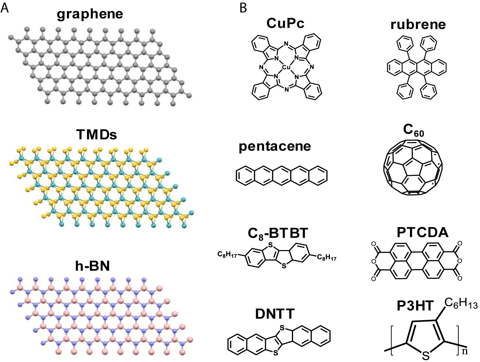
Figure 1. Structures of some commonly used (A) 2D materials and (B) OSCs for OSC/2D hybrid FETs.
Herein we emphasize on the recent progress of OFETs based on OSC/2D heterostructures from materials, film growth, electronic structure optimization, and device performance to gain a full view of the OSC/2D hybrid FETs. It is worth noting that OSC/2D heterostructures also show their potential in applications for many different kinds of organic optoelectronic devices such as OPVs and OLEDs, and they can also effectively improve device performances in many 2D material-based devices, and there have been several reviews summarizing such topics (Gobbi et al., 2018; Sun et al., 2019). Therefore, in this paper, we will focus on the work of OSC/2D hybrid FETs, especially with OSCs working as the main active materials for FET conductive channels. The review mainly introduces and summarizes the progress of three types of OSC/2D hybrid FETs according to the role of the 2D materials: (i) 2D materials work as growth templates for the highly ordered OSC layers; (ii) 2D materials are employed to optimize the electronic structure of the OSC conductive channels; and (iii) OSC/2D heterojunction FETs in which the band structures of the heterojunctions endow the device with specific opto-electronic functions, and some fundamental investigations on organic solid physics by OSC/2D heterostructures will also be included in this part. In the end, further discussion and outlook of this topic will be considered. Table 1 summarizes these typical OSC-2D heterostructures and their device applications.
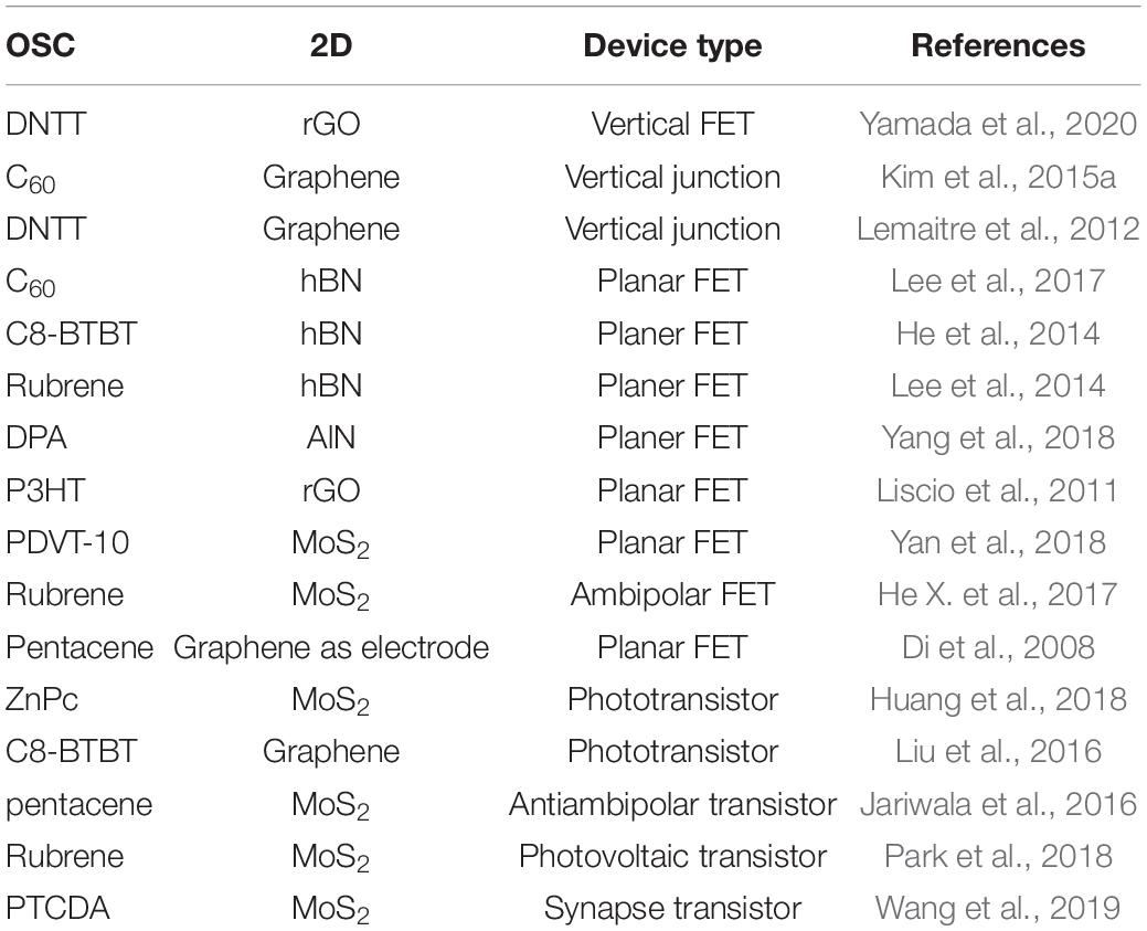
Table 1. Typical OSC-2D hybrid structure that has been utilized in FET research.
Prior to the introduction of the FET progress, we will briefly summarize the constructing method for OSC/2D heterostructures, details can be found in other reviews (Sun et al., 2019). For the OSC/2D heterostructure, their different thermal and chemical properties make it hard to fabricate through one step or one method. Thus it usually takes two steps to complete the fabrication. Two-dimensional materials are usually obtained from CVD growth or exfoliated from bulk crystals, the major task lies on the successful growth of OSC films on these 2D materials. The deposition of OSC on the 2D materials can be through vacuum sublimation or solution processing. Two kinds of vacuum sublimation methods have been employed to grow organic molecules on 2D materials. One typical approach is directly thermal evaporating organic molecules from a evaporator to the 2D materials which are placed in a sample holder above the evaporator (Wang and Hersam, 2009; Dou et al., 2011; Emery et al., 2011; Mao et al., 2011; Lemaitre et al., 2012; Singha Roy et al., 2012; Kim et al., 2015a, b; Nguyen et al., 2015, 2020; Zheng et al., 2016). Another technique is physical vapor transport, that is when the organic powder is placed in a vacuum tube where the substrate with the 2D materials is placed in the same tube with a distance of several inches away from the organic powder, during which carrier gas can be employed or not (He et al., 2014; Lee et al., 2014, 2017; Yang et al., 2018). For both methods, one common issue is that the organic semiconductor with a large conjugated unit tends to adopt face-on orientation initially, which usually is not favorable for common OFET transport. A good point is that several organic semiconductors could transfer to edge-on orientation from the second layer on the 2D materials after the initial face-on layer formed. This growth manner enables the growth of high quality ultra-thin organic film crystals with efficient transport to 2D materials (He et al., 2014). Some semiconductors such as Rubrene or C60 could directly grow into favorable film morphology owing to the non-planar or isotropic structure (Lee et al., 2014, 2017). Introducing a surface treatment method also could avoid the face-on orientation and yield high quality film growth. Also utilizing the lying-down packing of organic molecules on 2D materials, a research group obtained unique vertically grown nanocrystals through growth optimization, which present promising functions in photovoltaic or vertical transistors (Zhang Y. et al., 2014). The deposition of organic semiconductors through a solution processing approach is another common effect path. Spin-coating, dip coating, or drop-casting has been employed to construct OSC/2D hybrid structures for both small molecules and polymers. During the solution process, the molecule orientation is critically related to the deposition conditions. In the fast spin-coating process, the film morphology was hardly influenced by the substrates. However, in the slow solution process the growth process of face-on orientation in organic semiconductors was still preferred owing to the strong molecule-2D surface interaction. Interestingly, utilizing this, some researchers could achieve the vertical aligned organic nanowires through the solution phase epitaxy technique (Wang et al., 2015; Zheng et al., 2016).
OFETs Based on OSC/2D Hybrid Structures
OSC/2D Hybrid FETs With 2D Materials as Growth Templates for OFET Channel Layers
In the early stages of the study on OSC molecules growth, single crystal substrates were widely adopted following the epitaxial growth technologies of inorganic semiconductors. Although 2D lattices of molecules can be obtained on various kinds of single crystal substrates, such as NaCl, metals, and highly ordered pyrolytic graphite (HOPG), the molecules usually adopt a face-on manner on substrates, that is, the π-π conjugated plane of the molecules parallel to the substrates (Forrest, 1997; Hooks et al., 2001). The superior charge transport direction of such structures is normal to the substrate which contradicts the parallel transport in conventional FET devices (Yang and Yan, 2009; Lee et al., 2011; Yang et al., 2015; Yamada et al., 2020). More importantly, this film phase is a metastable state under a large amount of stress which is formed driven by the strong molecule-substrate interaction. Therefore, with the increase of film thickness the film structure will change due to stress relaxation (Witte and Wöll, 2011). The emergence of 2D materials provides the possibility that they offer in-plane templates and weak molecular-substrate interactions.
As the first 2D material and the single layer of HOPG, graphene was employed for the template growth of OSCs in many studies. Wang and Hersam (2009) observed that perylene-3,4,9,10-tetracarboxylic dianhydride (PTCDA) can self-assemble into stable, well-ordered islands and monolayers with a herringbone arrangement at room temperature on an epitaxial graphene grow on an SiC(0001) surface using scanning tunneling microscopy (STM). The face-on structure closely resembles its formation on graphite (Figure 2A; Wang and Hersam, 2009; Emery et al., 2011). Mao et al. (2011) also found that the molecular orientation of chloroaluminum phthalocyanine (ClAlPc) changes from random arrangement on a bare indium tin oxide (ITO) substrate to the lying-down manner on the chemical vapor deposition (CVD) graphene modified ITO with improved charge transport efficiency along the direction perpendicular to the ITO surface (Figure 2B). In addition, in situ ultraviolet photoelectron spectroscopy (UPS) spectra proved that ClAlPc molecules adopted identical packing on HOPG (Dou et al., 2011). Similar face-on orientations on graphene were also found in many other OSC molecules, such as copper phthalocyanine (CuPc) (Singha Roy et al., 2012), pentacene (Kim et al., 2015b; Nguyen et al., 2015), and 9,10-bis(phenylethynyl) anthracene (BPEA) (Zheng et al., 2016; Figures 2C,D). Although the OSC molecules in the above work form laterally ordered films with certain epitaxial relationships, these planar hetero-films with OSC molecules lying down on graphene are difficult to fabricate with conventional FET devices requiring the superior charge transport direction of the films parallel to the substrate. Moreover, when the source-drain bias is applied, the conductive channel of such films will be occupied by the metallic graphene layer other than the OSC layer and results in insufficient Ion/Ioff values for a transistor device. A feasible solution for the mentioned problems is to employ an unconventional transistor architecture, vertical FETs (VFETs). As illustrated in Figures 3A,B, a VFET device can be regarded as a vertical diode device constructed on a dielectric/electrode substrate, with the additional electrode working as the gate terminal to modulate the diode current by manipulating the contact barrier of the diode. This device configuration is very compatible with organic light emitting diodes (OLEDs), and thus is a good candidate for driving circuits for OLED displays as well as its large output current density. The OSC/graphene VFET takes advantage of both the vertical charge transport direction and the metallic nature of graphene as source electrodes. Lemaitre et al. (2012) constructed a VFET device employing a 500 nm dinaphtho-[2,3-b:20,30-f]thieno[3,2-b]thiophene (DNTT) crystalline film as the conductive channel deposited on transferred CVD grown graphene sheets with controllable pore density from 0 to 20%. The devices with a graphene pore density of 20% that possess both a barrier height lowering and a tunnel barrier thinning exhibit the best performance of an Ion/Ioff value exceeding 106 and output current density of 200 mA/cm2 at a low drain voltage of 5 V. Compared with the devices with carbon tubes as the source electrode (CN-VFET), the DNTT/graphene devices (G-VFET) showed significantly smaller hysteresis, much larger Ion/Ioff values and output current density (Figure 3C), due to the plane-like morphology and lower impedance of the monolithic graphene layer. Bao et al. employed the template-grown fullerene (C60) films on graphene to fabricate n-type transport VFET devices (Kim et al., 2015a). With strong epitaxial relations between C60 and graphene lattice directions, a uniform morphology of C60 film on graphene with a grain size as large as 500 nm can be obtained, as shown in Figures 3D,E. VFETs based on such ordered films exhibit an on/off ratio above 3 × 10³ at a drain voltage of 2 V with a modulation of C60/graphene barrier over 0.3 eV by applying gate bias (Figures 3F,G). Recently, Cho and coworkers electronically doped the graphene template to suppress the charge transfer between C60 and graphene during the growth of C60 and realized the growth of highly ordered layer-by-layer C60 films without Fermi-level pinning with graphene (Figure 3H; Nguyen et al., 2020). A conventional planar FET device based on these C60 films which were transferred to an SiO2/Si substrate showed a maximum mobility of 2.5 cm2/Vs, and the VFET device based on such a C60/graphene heterostructure showed efficient tunability of the charge injection barrier, approaching the Schottky–Mott limit (Figures 3I,J).
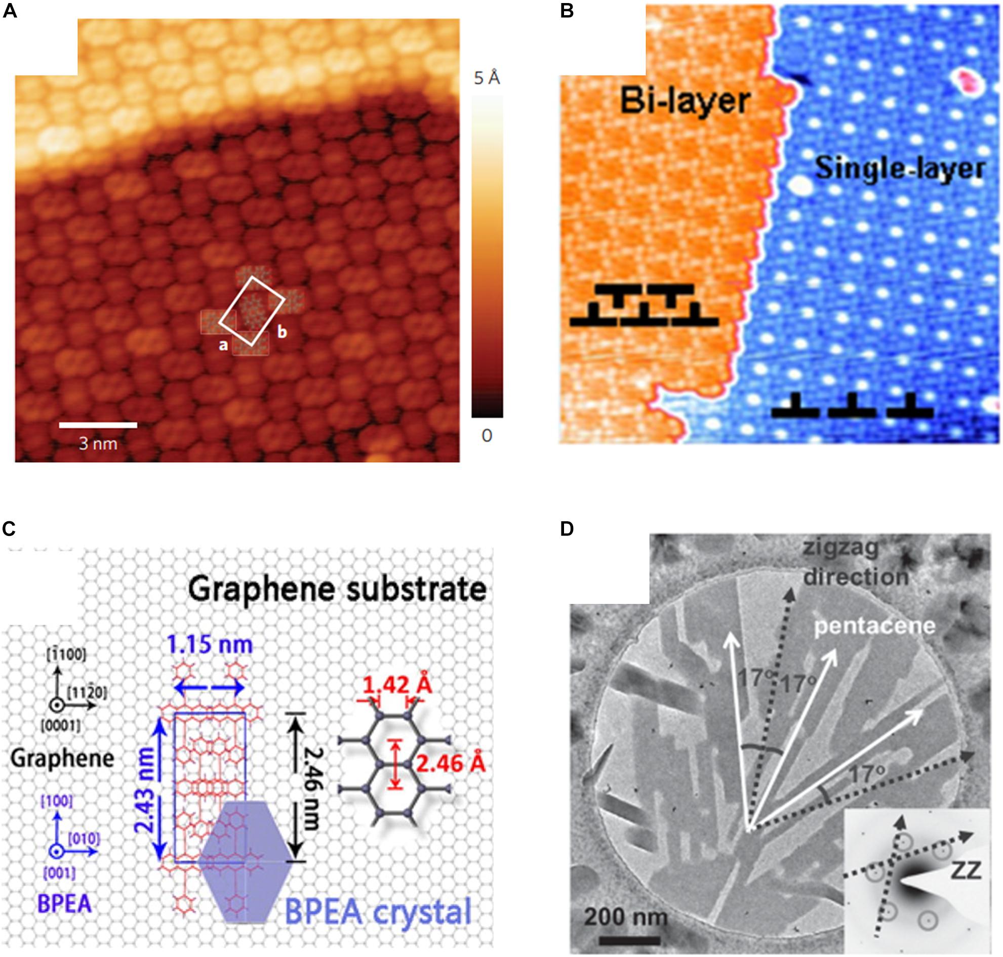
Figure 2. Template growth of OSCs on graphene. (A) Molecular-resolution STM image of the PTCDA monolayer on graphene. Reproduced from Wang and Hersam (2009) with permission from Copyright 2009 Springer Nature. (B) STM image ClAlPc films on graphene including the single layer and bilayer packing. Reproduced from Mao et al. (2011) with permission from Copyright 2011 American Institute of Physics. (C) Schematic illustration of the lattice and epitaxy relationship between BPEA and graphene. Reproduced from Zheng et al. (2016) with permission from Copyright 2016 American Chemical Society. (D) TEM image of different areas where pentacene shows non-parallel crystal axis directions. Inset shows the electron diffraction of the underlying graphene membrane. Reproduced from Singha Roy et al. (2012) with permission from Copyright 2015 Wiley.
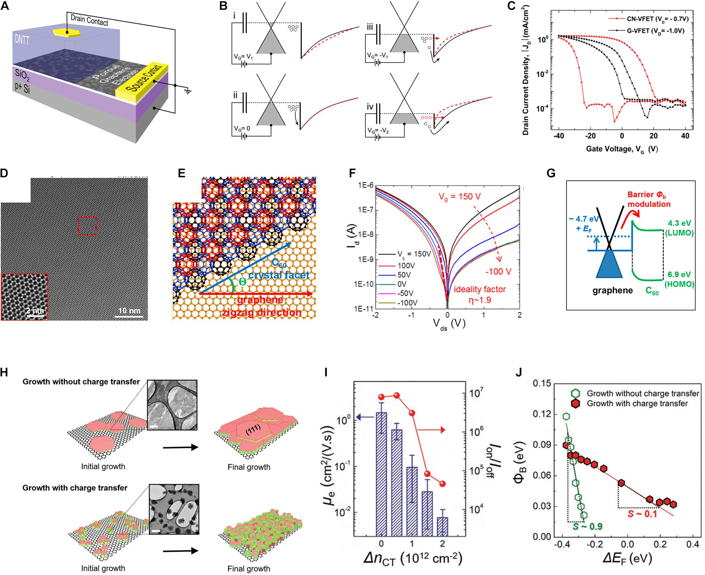
Figure 3. OSCs/graphene based VFETs. (A) Device configuration of DNTT/graphene VFET. (B) Energy level diagram at the graphene-semiconducting channel interface for different bias situations. (C) Transfer curves for a CN-VFET and the G-VFET with a 20% areal hole density electrode. Reproduced from Lemaitre et al. (2012) with permission from Copyright 2012 American Chemical Society. (D) TEM image of C60 film on graphene. (E) C60 crystal packing on graphene. (F) Output curve with different applied gate voltages. (G) Energy diagram of the graphene/C60 heterostructure. Reproduced from Kim et al., 2015a with permission from Copyright 2015 American Chemical Society. (H) Schematic diagram of C60 crystal growth on graphene without (upper) and with (lower) the charge transfer between them. Insets: TEM images of corresponding graphene–C60 samples on TEM grids. (I) Plots of transistor parameters of C60-FETs vs. the number of transferred electrons (ΔnCT) during C60 growth. (J) The Schottky barrier height (ΦB) vs. ΔEF. Reproduced from Nguyen et al. (2020) under the Creative Commons CC BY license.
Despite of the above achievements, non-metallic template materials are still desirable for the common planar OFET geometry. Two-dimensional hexagonal boron nitride (h-BN) is promising for satisfying such a requirement because it is nearly insulated with a wide bandgap of approximately 6 eV as well as the absence of dangling bonds and charge traps. 5,6,11,12-Tetraphenylnaphthacene (rubrene) shows ultrahigh carrier mobility and band-like transport behavior in its singe crystal FET, while crystalline films were difficult to obtain on amorphous substrates such as SiO2/Si. Kim and coworkers realized highly ordered rubrene crystals on exfoliated h-BN crystals through a vapor-phase transport growth method (Figures 4A,B; Lee et al., 2014). Selected area electron diffraction (SAED) patterns of the rubrene film and the underlying h-BN crystal demonstrates an epitaxial relationship between the two crystals with an angle of ca. 4° between their a-axes (Figure 4C), and a grazing-angle x-ray diffraction (GIXD) of rubrene showed a 6-fold symmetry which suggests the rubrene crystals as grown are epitaxially locked in the crystallographic direction of the 3-fold symmetric h-BN crystal. Polarized optical microscopy images at different angles indicate that the rubrene crystal on a h-BN flake is a single domain with the size determined by the underlying h-BN flakes as shown in Figure 4D. The crucial role of h-BN in the template growth of rubrene can be prominently reflected that on one hand the relatively weak molecule-substrate interactions that allow the structural parameters of the rubrene crystals on h-BN to be close to those of free-standing rubrene crystals; on the other hand the interaction is strong enough to provide epitaxial registry between the two atomic lattices. Such high quality rubrene crystals were used to fabricate transistor devices with transferred graphene films as source/drain electrodes. The devices showed substantially high average and maximum mobility values of 5.1 ± 2.7 cm2/Vs and 11.5 cm2/Vs which are comparable to single crystal devices (Figure 4E), accompanied by negligibly small hysteresis and high Ion/Ioff ratio of 106. This performance highlights the merits of template grown OSC layers on 2D materials as channel materials for OFETs. Using CVD grown h-BN as a growth template, Lee et al. (2017) obtained highly ordered crystalline C60 films. Transmission electron microscopy (TEM) imaging and SAED patterns of the C60 films and h-BN crystal prove a mild rotational alignment effect between the lattice of h-BN and the C60 crystallographic direction. The topography and phase images as well as GIXD data demonstrated a significantly improved ordering compared to the films grown on the SiO2/Si substrate (Figure 4F). As shown in Figures 4G,H, the OFET device based on this C60/h-BN film exhibited high average mobility and maximum values of 1.7 and 2.9 cm2/Vs, respectively, which is 40 times higher than those of C60 on SiO2. The high C60 film quality, as well as the low roughness and trap density of the h-BN surface should be responsible for the high device performance. He et al. (2014) realized a monolayer OFET device with h-BN as the growth template for another typical high-mobility OSC molecule, dioctylbenzothienobenzothiophene (C8-BTBT). This monolayer OFET showed impressive performance, with the room temperature peak field-effect mobility reaching ∼10cm2/Vs, much higher than that of previous monolayer OFETs and comparable to some 2D materials such as MoS2. Moreover, the successful realization of a high-performance monolayer FET can skip the common non-linearity at low bias and attain complete saturation with extremely low pinch-off voltage of approximately 1 V. In the above work, h-BN is proven a good growth template for different molecules to achieve highly ordered, even single-crystal-like crystalline films due to a moderate interaction with molecules and to assemble in a manner close to their free-standing single crystal structures with sufficiently large size. In addition, the ultra-smooth and dangling-bond-free surface of the 2D h-BN effectively reduce trap density and avoid disturbing the charge transport of OSC crystals, which is also profitable for enhancing OFETs performance.
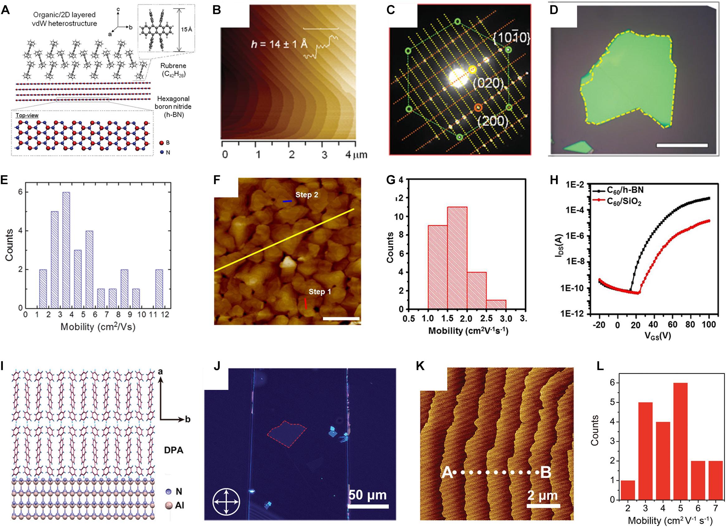
Figure 4. OSCs/2D hybrid FETs with 2D materials as growth templates and insulating layers. (A) The packing mode of the rubrene/h-BN heterostructure. (B) AFM height image of the rubrene terraced film. A step height of 14 ± 1 Å is indicated. (C) Bright-field TEM image and selected-area electron diffraction pattern of the rubrene crystal grown on h-BN. The orange, yellow, and green circles corresponds to (200)rub, (020)rub, and h-BN planes, respectively. (D) Large single-crystalline domain of rubrene crystalline films grown on h-BN flakes by polarization optical characterization. The scale bar is 20 μm. (E) Histogram of mobility of rubrene/h-BN OFET devices with graphene contacts. Reproduced from Lee et al. (2014) with permission from Copyright 2014 Wiley. (F) AFM height images for C60 on CVD h-BN. (G) Histogram of electron mobilities of C60 FETs on h-BN. (H) Comparison of transfer curves from C60 FETs on h-BN vs. on SiO2. Reproduced from Lee et al. (2017) with permission from Copyright 2017 American Chemical Society. (I) Schematic packing mode image of DPA molecules on the AlN crystal surface. (J) Cross polarized optical micrographs of the DPA crystals. (K) AFM height images of the DPA crystal surface. (L) Statistical distribution of the saturation mobility of the OFETs based on the AlN/DPA crystalline heterostructures. Reproduced from Yang et al. (2018) with permission from Copyright 2018 Wiley.
However, new types of insulting templates are still in demand for the epitaxial growth of various OSC molecules. Moreover, a single crystal h-BN is usually fabricated by exfoliation with a relatively small domain size, while a CVD grown h-BN is polycrystalline and limits the film quality of templated OSC layers. Hexagonal aluminum nitride (h-AlN) is also a III-V compound with a wide band gap of 6.2 eV similar to a h-BN, and its higher dielectric permittivity enables us to realize OFETs with low power consumption. However, AlN single-crystals have not yet been reported as a gate dielectric due to the lack of an ideal 2D morphology that combines a thin thickness and a large lateral dimension. Yang et al. (2018) reported a 2D AlN crystal fabricated by a physical vapor transport method for the first time. The lateral dimensions of the 2D AlN range from hundreds of microns to a few millimeters, with a thickness between 200 and 400 nm. On this 2D AlN surface, single crystal domains of 2,6-diphenylanthracene (DPA) with lateral dimension up to tens of micrometers can be obtained, as indicated by cross-polarized microscopy and AFM (Figures 4I–K). The OFET device based on a van der Waals DPA/AlN single-crystalline heterostructure exhibited an excellent performance of saturation mobility of 6.8 cm2/Vs (Figure 4L), a high on/off current ratio of 108, and a steep subthreshold slope (SS) of 104 mV/dec. Importantly, such a result was obtained at a low operating voltage of −5 V, which profits from the high dielectric constant of 12.2 of 2D AlN.
In addition to the above mentioned template growth of small conjugated molecules on 2D materials, the improvement on the ordering of polymer films by 2D materials was also reported (Zhang et al., 2015; Chae et al., 2017). Zhang et al. (2015) found that in the poly(3-hexylthiophene) (P3HT)–molybdenum disulfide (MoS2) composite solutions, the interaction between P3HT and MoS2 can enhance the inter-chain ordering of P3HT under sonication, which may lead to high crystallinity of thin films. The AFM images and GIXD profiles of pristine P3HT, ultra-sonicated P3HT, and P3HT-MoS2 films confirmed that the MoS2 sheets induced the crystallization of P3HT. Consequently, the device performance of the P3HT OFET was significantly improved with a 38-fold enhancement on hole mobility and one order of magnitude increase of on/off current ratio.
OSC/2D Hybrid FETs With 2D Materials Optimizing the Electronic Structure of the OFET Conductive Channel
Distinct from traditional inorganic semiconductors, in which charge carrier concentration is mainly determined by chemical doping, OSCs usually exhibit a very low intrinsic carrier concentration due to the molecular conductive mechanism. The carrier mobility is highly dependent on the free carrier concentration in the conductive channel of OFETs derived from the hopping charge transport mode, in which the charge carriers repeat the process of being captured and are released by the unfilled traps during the transport (Vissenberg and Matters, 1998; Podzorov et al., 2004). Thus, competition between the concentration of electrode-injected carriers and the density of electrical traps originating from the organic solids (such as defects or impurities) or organic/dielectric interface (such as surface chemical groups) plays an important role in determining the device performance of OFETs. Therefore, optimizing the electronic structure of the conductive channel by reducing trap density, increasing carrier concentration, and enhancing carrier injection efficiency is an important strategy for promoting the device performance of OFETs.
Bulk doping made great progress for devices based on polymer or amorphous films, such as OPVs, OLEDs, and polymer based OFETs (Lussem et al., 2016; Salzmann et al., 2016; Wang et al., 2018). Liscio et al. (2011) proposed to utilize high conductivity of the reduced graphene oxide (RGO) to improve the charge transport of P3HT films by employing RGO sheets as percolation pathways in OSC-RGO blends. P3HT films were coated on a discontinuous layer of atomically thin graphene sheets deposited on a SiO2 substrate in advance (Figure 5A). When the FET is operating, the conductive RGO sheets act as preferential paths through which charges can travel much better than in pure P3HT and thus reduce the effective channel length of the transistor (Figure 5B). As a result, the hole mobility of the RGO–P3HT blends improved significantly with the increase of RGO coverage (Figure 5C). However, when this coverage increases to a certain value (42%), the conductive channel of the FET device will be dominated by the continuous RGO sheets, and this leads to poor gate modulation. Overall, the presence of an intermediate coverage of RGO can effectively promote the charge carrier mobility without diminishing the value of Ion/Ioff. Meanwhile, an improvement on hysteresis is also achieved with the addition of RGO sheets. To improve the charge transfer doping efficiency between OSCs and 2D materials, Lyuleeva et al. (2018) modified the surface of 2D silicon nanosheets (SiNSs) with various molecules to adjust the electrical characteristics of P3HT. Functionalized SiNSs, SiNS–C12H25, SiNS-styrenyl(SiNS–PhAc), and SiNS-2-(3-hexylthiophene-2-yl)vinyl (SiNS–ThAc) were synthesized with a microwave-assisted thermal initiated hydrosilylation reaction (Figure 5D). The composite solutions of P3HT with different functionalized SiNSs were spin-coated on Si/SiO2 substrates to fabricate electrolyte-gated field-effect transistors (EGFETs, see device architecture in Figure 5E), which are promising for the application for bio-sensors. The SiNS–ThAc/P3HT hybrid film showed the most promising results with the values of ID,max and transconductance and mobility was approximately three to four times higher compared to pure polymer devices (Figure 5F). In addition to the fact that the SiNS–ThAc/P3HT film owns the best miscibility among all the hybrid films which facilitate charge transport, the doping effect between P3HT and the silicon nanosheets characterized by electron paramagnetic resonance (EPR) measurements, plays an important role in promoting device performance in the following manner depicted in Figure 5G: the charge carriers can transfer from the P3HT polymer chain onto the thiophene group of SiNS–ThAc due to the electronic connection between the thiophene group and the SiNS, and the transport within the two-dimensional silicon nanosheets improves the charge transport efficiency to another P3HT chain, no matter if it is on one side of the sheet or on the other side. Moreover, the thiophene group of the SiNS–ThAc could possibly interact with two P3HT polymer chains, also enhancing the charge transport between different polymer chains. In the above cases, 2D material sheets as bulk dopants were demonstrated to significantly improve the OFETs performance by acting as highly conductive islands in OSC films to promote the hopping efficiency.
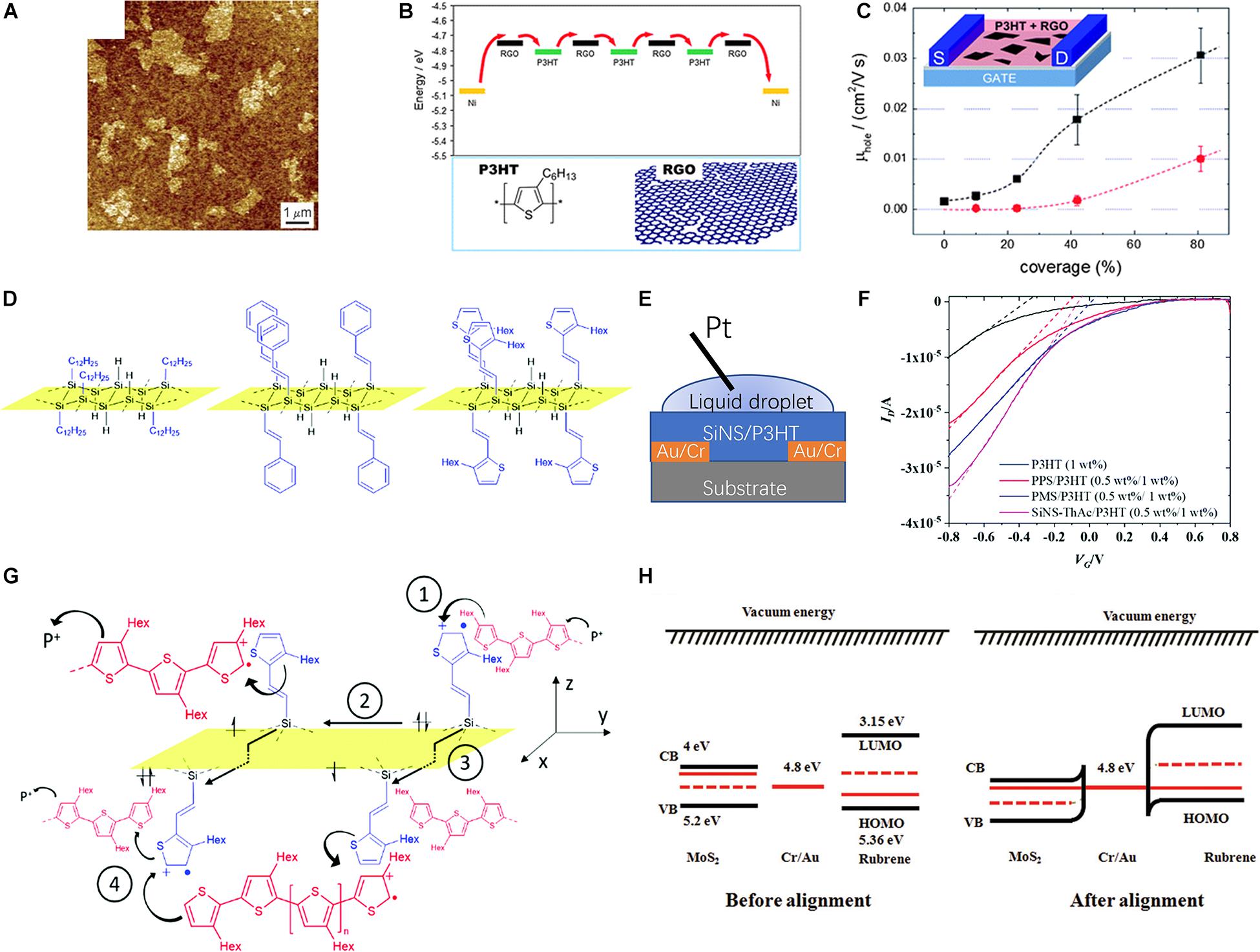
Figure 5. OSCs/2D hybrid FETs with 2D materials as dopants. (A) AFM images of RGO sheets deposited on a native SiO2 substrate, and covered by a thin film of P3HT. (B) Schematic representation of the energy diagram and charge transport in the device. Inset below shows structures of RGO and P3HT. (C) Hole mobility vs. coverage for RGO and RGO + P3HT FETs. Reproduced from Liscio et al. (2011) with permission from Copyright 2011 the Royal Society of Chemistry. (D) Structures of the SiNSs. (E) EGFET device configuration. (F) the transfer curves (solid lines) and the linear fitting. (G) Possible electronic transportation model in SiNS–ThAc/P3HT hybrid films. Reproduced from Lyuleeva et al. (2018) with permission from Copyright 2018 the Royal Society of Chemistry. (H) Band diagrams of rubrene, MoS2, and source–drain electrode before alignment (left) and after alignment (right). Reproduced from Wang and Yan (2010) with permission from Copyright 2017 Wiley.
Compared to bulk doping, interface doping with a parallel heterojunction structure is a more common approach to tune the electronic structure of conductive channels in OFETs, especially for single crystals or crystalline small molecule films, in which bulk doping tends to disturb the crystal or film ordering and dramatically reduces the device performance. Many cases of interface doping between OSC p-n heterojunctions have been proven to significantly increase the major charge carrier concentration or reduce the interface trap density and accordingly promote device performance (Wang and Yan, 2010). Therefore, OSC/2D p-n heterojunctions are also expected to facilitate the OFETs performance. However, so far the constructed OSC/2D p-n heterojunctions seldom exhibited a favored interface doping type to promote major charge carrier concentration of OSC channels as in many organic-organic systems. The Zhu group constructed a parallel p-n heterojunction FET with a p-type OSC poly[2,5-bis(2-decyltetradecyl)pyrrolo[3,4-c]pyrrole-1,4(2H,5H)dione-alt-5,50-di(thiophen-2-yl)-2,20-(E)-2-(2-(thiophen-2-yl)vinyl)-thiophene] (PDVT-10) and an n-type 2D material MoS2 (Yan et al., 2018). The device was fabricated by transferring a CVD grown MoS2 film on top of ∼9 nm thick PDVT-10 film on the OTS-treated Si/SiO2 substrate and exhibited typical ambipolar transport characteristics with an increased hole mobility by nearly one order of magnitude. The rectification effect of the MoS2/PDVT-10 junction evidenced that it is a traditional depleted p-n junction with major charge carriers depleted in the junction region. Similarly, in the single crystal rubrene/MoS2 p-n heterojunction FET fabricated by He X. et al., 2017 despite that the device exhibited a high level of ambipolar charge transport (a hole mobility of 1.27 cm2/Vs and an electron mobility of 0.36 cm2/Vs at a drain bias of 0.5 V), a depleted heterojunction was believed to be established between rubrene and MoS2 as suggested from their energy band alignment illustration (Figure 5H). Although so far a major carrier accumulated heterojunction between OSCs and 2D materials has rarely been reported, the abundant selection and tunable electronic structure of both OSCs and 2D materials are still promising in the application of such a method in high-performance OFETs (Petoukhoff et al., 2019).
Electrode material is also important for OFETs, since the injection barrier between the source and OSCs can severely affect the device performance. In addition, flexibility and transparency are now required for electrode materials aiming to create novel smart or wearable devices. Metallic 2D materials are among the popular candidates to satisfy these new demands. Except for graphene (Di et al., 2008), MXene also shows great potential. Cho and coworkers employed two-dimensional Ti3C2Tx MXene as electrodes to realize a high-performance OFETs array with both p-type and n-type OSCs, and flexible complementary logic circuits, such as NOT, NAND, and NOR, were fabricated via integration of p-type and n-type OFETs (Figures 6A,B; Lyu et al., 2019). In this work, the MXene not only exhibited its capability of acting as a highly conductive flexible electrode, but also played a crucial role in improving OFETs performance by lowering the carrier injection barrier. Figure 6C displays the performances of the p- and n-type OFETs with the Ti3C2Tx MXene electrodes. The Ohmic contact between MXene and the p-type OSC, pentacene, resulted in a good performance for the pentacene FET with an average mobility of 0.95 cm2/Vs, Ion/Ioff of 1.6 × 10⁷, and an average threshold voltage of −12.9 V. To lower the injection barrier to the n-type OSC, N,N′-dioctyl-3,4,9,10-perylenedicarboximide (PTCDI-C8), the work function of the MXene electrodes was effectively modulated via chemical doping with NH3. Using NH3–doped MXene electrodes, the n-type OFET performance is drastically improved: the average μ of the devices increased from 0.21 to 0.65 cm2/Vs, the average threshold voltage decreased from 54.2 to 17.0 V, and the average Ion/Ioff increased from 2.9 × 10⁶ to 5.1 × 10⁶. This work demonstrates that 2D materials can also work well as flexible electrodes for OFETs with efficient charge injection.
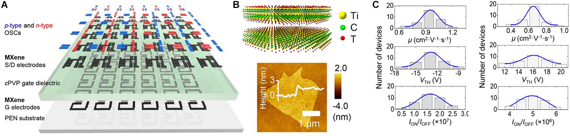
Figure 6. OFETs with 2D materials as electrodes. (A) Schematic image of the OFET device array based on Ti3C2Tx MXene electrodes. (B) Crystal structure of MXene (top) and AFM image of the monolayer MXene on the SiO2 substrate (bottom). (C) Histogram and normal distribution of electrical properties of p-type pentacene OFETs with MXene electrodes (left) and n-type PTCDI-C8 OFETs with NMX electrodes (right). Reproduced from Lyu et al. (2019) with permission from Copyright 2019 American Chemical Society.
The strategies to optimize the electronic structure of the conductive channel of OFETs devices presented in the above work can be summarized in the following manner: (i) employing 2D material nanosheets to construct charge transport pathways with higher conducting efficiency in the bulk of OSC layers (Liscio et al., 2011; Lyuleeva et al., 2018); (ii) establishing ambipolar OSC/2D hybrid FETs with parallel layers of OSC and 2D materials respectively working as n-type or p-type conductive channels (He X. et al., 2017; Yan et al., 2018); (iii) reducing the contact barriers between OSC channels and electrodes with proper 2D materials as source/drain electrodes (Di et al., 2008; Lyu et al., 2019). In addition, interface charge transfer doping between OSC and 2D layers is also of great potential to optimize the channel electronic structure and improve the OFETs performances.
Multi-Functional OSC/2D Hybrid FETs
In the above section, the source-drain current in the organic/2D heterojunction mainly drifted in the direction parallel to the heterojunction instead of flowing across the junction region. In this part we will introduce some research on organic/2D heterojunction FETs which utilize interface band structures of heterojunctions. When the interface band structures of the organic/2D heterojunction are taken in consideration, various opto-electronic effects will emerge and can be employed to construct many different types of opto-electronic devices (Xu et al., 2013; He et al., 2015; Gu et al., 2017; Sarkar and Pal, 2017; Gonzalez Arellano et al., 2018; Habib et al., 2018; Huang et al., 2018; Zhang et al., 2018). The following summarizes some organic/2D heterojunctions arranged in FET device structures with various additional functions as well as some fundamental research on the physics of OSC solids using the platform of organic/2D heterojunctions.
It has been mentioned before that type II heterojunctions can be established in many organic/2D structures, and such an interface band structure can be employed to separate electron-hole pairs or excitons to free carriers. Moreover, many 2D materials and OSCs show high excitonic absorption and are widely utilized in photo-electric devices such as photodetectors or photovoltaics. Therefore, these functions can be combined with OFETs based on organic/2D heterojunctions for further modulating the device performances. Liu et al. (2015) exploited a fast response photodetector based on a single crystal rubrene/MoS2 heterojunction FET. A 300 nm thick sample of single crystal rubrene was positioned on 5 nm MoS2 thin flakes which were exfoliated on a SiO2/Si substrate prior and constructed a partially overlapped conductive channel. The FET device displayed a gate voltage-tuned current rectification behavior originating from an FET channel consisting of two p and n semiconductors in series: the source-drain current reached maximum when the low-conductive rubrene channel was switched on under negative gate biases (Figure 7A). This device exhibited good photo-response properties with a photoresponsivity of ≈ 500 mA/W and a fast response time of less than 5 ms to the 532 nm laser, which are prominent compared to many other 2D material systems (Figures 7B,C). The characteristic gate tunability of OFETs can be utilized to modulate the photo response performance. The Wang group utilized epitaxially grown C8-BTBT films on graphene to realize a high-efficiency phototransistor with photoresponsivity up to 1.57 × 10⁴ A/W, short response time of 25 ms, and photoconductive gain over 108 to the 355 nm laser (Liu et al., 2016). C8-BTBT films as the photo absorption layer were thermally deposited on pre-patterned graphene FETs with Au electrodes, and the positive shift of the charge neutrality point of graphene proved the establishment of charge transfer and an accordingly built-in field which was responsible for the separating of electron–hole pairs. The gate bias can modulate the type and concentration of charge carriers in the underlying graphene and the maximum photoresponsivity. The device also exhibited a photo response dependence on the layer number of C8-BTBT films (Figure 7D). With the evolution of interfacial charge transfer efficiency, external quantum efficiency, response time, and photoresponsivity with layer number of C8-BTBT, the proposed mechanism suggested that the highly ordered organic layer and interface played a crucial role in the efficient photo detection. This work demonstrates the advantage of the unique feature from epitaxial OSC/2D heterojunctions, the high quality of organic crystal and interface, in device applications. The capacity of OSC/2D heterojunctions for separating excitons also shows applications in photovoltaics. Jariwala et al. (2016) fabricated a p-n OSC/2D heterojunction with pentacene and MoS2 which exhibited gate tunable charge transport characteristics and photovoltaic effects. The conductive channel of the FET device is composed of 40 nm pentacene films thermally deposited on the exfoliated two-layer MoS2 flake with a partial overlapped geometry. Output curves of this device showed gate tunable rectifying characteristics originating from the type II heterojunction, and the transfer curves exhibited the asymmetric anti-ambipolar behavior shown in Figure 7E. This heterojunction displayed a photovoltaic effect with an open circuit voltage VOC ∼ 0.3 V and a short circuit current -ISC ∼ 3 nA, coupled with a gate bias dependent ISC (Figure 7F). Scanning photocurrent microscopy (SPCM) images depicted the photocurrent maximum, traced the MoS2 flake boundary, and suggested that the photovoltage arose from the pentacene/MoS2 junction. Electrostatic force microscopy (EFM) further described the band alignment of the junction interface (Figures 7G,H). Such pictures will help us to gain deep insight on the OSC/2D heterojunctions and extend their applications. A photovoltaic FET device was also realized in a single crystal rubrene/MoS2 heterojunction by Park et al. (2018). Except for the anti-ambipolar transport and the gate tunable photovoltaic effects, this heterojunction exhibited photovoltaic gate-field-controlled transistor characteristics, in which the transistor was operated by a gate tunable ISC driven by light irradiation without source-drain bias. The device characteristics and operating mechanism are displayed in Figures 7I,J. This work showed the potential for energy-saving optoelectronic devices.
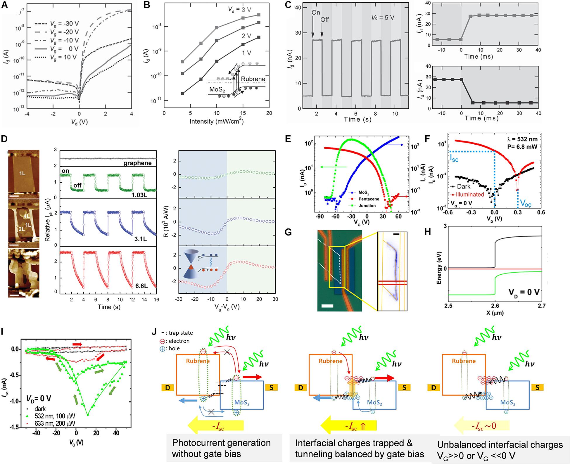
Figure 7. Photodetector and photovoltaic OSC/2D hybrid FETs. (A) The output curves of the MoS2-rubene p-n junction. (B) Photocurrent as a function of incident laser intensity under different drain voltages. The inset shows the schematic for the photocurrent generation process of the p–n junction under light illumination. (C) Switch behavior of the MoS2/rubrene heterostructure. Reproduced from Liu et al. (2015) with permission from Copyright 2015 Wiley. (D) Photo-response of C8-BTBT/graphene phototransistors, and evolutions of the film morphology (left), dynamic photocurrent response (middle), and gate tunability (right) to photoresponsivity with increasing C8-BTBT thickness. Reproduced from Liu et al. (2016) with permission from Copyright 2016 Wiley. (E) Comparison of transfer characteristics between the single layer (pentacene and MoS2) and the pentacene/MoS2 heterostructure FETs. (F) Dark and illuminated ID−VD characteristics of the pentacene/MoS2 heterostructure at VG = 0 V. (G) Spatial photocurrent map at VD = 0 V of the region indicated. (H) Horizontal band profiles near the edge of the overlapped pentacene/MoS2 region (X = 2.6 μm). (I) Isc vs. VG characteristic curves of the MoS2/rubrene FET under dark conditions and light irradiation conditions. (J) Schematic illustrations of the photocurrent generation processes under focused laser irradiation at the MoS2/rubrene heterojunction under different bias conditions. Reproduced from Park et al. (2018) with permission from Copyright 2018 American Chemical Society.
In addition to the traditional opto-electronic devices, the OSC/2D heterojunction FETs were also employed to construct novel bio-electronic devices. Zhou and coworkers demonstrated a multi-functional synaptic transistor based on the PTCDA/MoS2 heterojunction (Wang et al., 2019). The device was designed with a top contact bottom gate PTCDA/MoS2 FET device as the postsynaptic in the synapse, the conductive channel was mainly dominated by the MoS2 layer due to its much higher conductivity than PTCDA (Figure 8A). With proper top gate bias or laser as the presynaptic, the band alignment of the heterojunction is manipulated, and the electron concentration in the MoS2 layer will be modulated by the charge transfer with the PTCDA layer and thus the source drain current is accordingly modulated (Figures 8B,C). Using this device, basic plasticity functions of biological synapses can be successfully mimicked and the potential of the OSC/2D heterojunction in constituting neural networks and brain-like computations are expected.
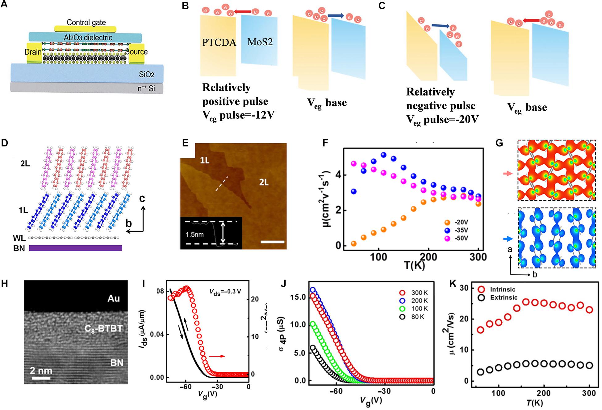
Figure 8. Bio-electronic devices based on OSC/2D heterojunctions, and fundamental studies on highly ordered OSC films grown on 2D templates. (A) Structure of the synapse device based on a MoS2/PTCDA hybrid heterojunction under electrical modulation. Operating mechanism of (B) inhibitory and (C) excitatory synaptic behaviors. Reproduced from Wang et al. (2019) with permission from Copyright 2019 Wiley. (D) Schematic illustration of the molecular packing of 1L and 2L pentacene on h-BN. (E) AFM image of 2L pentacene crystals on h-BN. Insets are the height profiles as indicated. (F) Mobility as a function of temperature under different VG. (G) Top views of the molecular orbitals of the intermolecular bonding states in the slices cleaved in the a-b plane for 1L pentacene (blue) and 2L pentacene (red). Reproduced from Zhang et al. (2016) with permission from Copyright 2016 American Physical Society. (H) Cross-sectional TEM image of an Au/C8-BTBT/h-BN stack, showing atomically smooth interface. (I) Room temperature double-sweep Ids-VG characteristics (black line) and the extracted four-terminal field-effect mobility as a function of VG (red circle) of the monolayer C8-BTBT/h-BN FET. (J) Channel conductance as a function of VG under different temperatures of the monolayer C8-BTBT/h-BN FET. (K) Extrinsic and intrinsic mobility as a function of temperature of the monolayer C8-BTBT/h-BN FET. Reproduced from He D. et al. (2017) under the Creative Commons CC BY license.
The OSC/2D heterojunctions cannot only be utilized to drastically promote the OFETs performance and construct various advanced functions, but can also offer a perfect platform for the fundamental research of OSC solid physics. Whether OSC solids bonded by weak van der Waals interactions can achieve band transport is important for both theory study and application development (Podzorov et al., 2004). Although some results provided positive evidence, this issue is still in debate (Podzorov et al., 2004; Troisi and Orlandi, 2006; Yang and Yan, 2009; Chang et al., 2011; Wang et al., 2014b). Deep insights can be provided with the recent research based on the single-crystal-like OSC domains grown on 2D templates (Cui et al., 2019). Wang and coworkers have made a series of reports on this topic. Few-layer crystals of a typical OSC, pentacene, were epitaxially grown on mechanically exfoliated hexagonal h-BN by the vapor transport method (Zhang et al., 2016). AFM, TEM, and SAED confirmed the establishment of a single crystalline monolayer to tetralayer pentacene crystals with a face-on interfacial or wetting layer attaching on the surface of h-BN, followed by the tilting first layer and standing up second layer as well as subsequent layers (Figures 8D,E). The large blue shift of exciton energy on the order of 0.3 eV compared to the free exciton state in pentacene thin films and monolayers indicated the highly delocalized nature of the template grown pentacene films due to their excellent crystallinity. Moreover, the high field-effect mobility approaching 3 cm2/Vs and the temperature-dependent electrical measurements directly suggested band-like transport for the second layer pentacene, while the first layer exhibited the signature of a 2D hopping transport (Figure 8F). This difference was attributed to the different degrees of molecular orbital overlaps along the a and b axes of pentacene crystals (Figure 8G). C8-BTBT, another OSC molecule exhibiting high OFET performance, was also proven to be epitaxially grown on h-BN and establish a highly ordered monolayer FET (He D. et al., 2017). Such devices demonstrate remarkable electrical characteristics, including intrinsic hole mobility over 30 cm2/Vs, Ohmic contact with 100 Ω⋅ cm resistance, and a band-like transport down to 150 K (Figures 8H–K). The 2D template-induced highly delocalized OSC system was also evidenced in C60 films grown on a black phosphorous (BP) substrate. Reduced inter-C60 distance and mutual orientation on BP can be directly observed in STM images, and scanning tunneling spectroscopy (STS) revealed that the C60 lowest unoccupied molecular orbital (LUMO) band was strongly delocalized in two dimensions. In addition, carrier mobility calculations predicted that such an electronic structure of C60 has a carrier mobility of ∼200–440 cm2/Vs. Such results could be quite important for constructing ultrahigh mobility OFETs. Monolayer OSC crystals obtained on 2D substrates offer new chances for physical study and device applications. The molecular packing of perylene derivative monolayers grown on BN provides an ideal condition for long-range J-aggregation with large unscreened dipole interactions and the suppression of charge-transfer processes. The films showed giant resonant absorption, bright photoluminescence emission, and a high photoluminescence quantum yield, as well as the evidence of super radiance at room-temperatures. Also, a light-emitting device with the monolayer J-aggregate was also demonstrated (Zhao et al., 2019). As to novel devices, a tunneling device with negative differential conductance based on the C8-BTBT/pentacene/graphene heterojunction was also realized (Zhang et al., 2017). The above work demonstrates that highly efficient charge transport can be obtained by highly ordered OSCs and OSC/2D heterojunctions can provide a path for new physics and device structures.
Discussion and Perspectives
As new classes of semiconductor materials have emerged in recent decades, besides the conventional opto-electronic applications, both OSCs and 2D materials show great potential in being applied to the novel smart devices proposed lately, such as wearable or bio-electronic devices, and thus the combination of OSCs and 2D materials could be a more promising candidate for such demands. In addition, the structural and electronic properties shared by the two materials, such as a dangling-free surface and tunable electronic structures, make the efficient combination of OSCs and 2D materials feasible and attractive. The recent studies have demonstrated the advantages of the employment of OSCs-2D hybrid structures in OFETs, which can be summarized from the aspects of film quality, electronic structure of the conductive channel, and advanced functions based on OSCs/2D heterojunctions:
(1) The OSC film ordering and, accordingly, the OFETs performances can be markedly improved in the presence of 2D materials. For small π-conjugated molecules, the epitaxial growth enabling highly ordered, even single-crystal-like films is facilitated by 2D materials serving as growth templates. Two-dimensional nanosheets also showed the capacity of drastically promoting the polymer-based FETs by enhancing the inter-chain ordering and association of polymers.
(2) Using 2D materials as highly conductive islands dispersed in OSC films, the charge transport efficiency in the conductive channel of OFETs showed an intensive progress. Meanwhile, the flexibility and tunable work function of 2D electrodes make high-performance OFET circuits highly achievable.
(3) The various band structures of the OSC/2D heterojunctions encourage multiple advanced functions of OFETs. Excitons generated by illumination can be separated by the OSC/2D heterojunction interface, allowing photodetection or photovoltaics to be endowed in OFET devices with gate tunable performance. In addition, the OSC/2D interface can also be manipulated for bio-electronic devices or fundamental physics investigations.
Except for the capability of improving OFET device performances, the OSCs/2D heterojunctions also offer new opportunities for the development of OFETs. Ultrahigh-mobility OFETs can be expected with highly ordered OSC films on 2D substrates exhibiting band-like charge transport behaviors. Also, ultrashort channel FETs or tunneling devices based on OSCs/2D heterojunctions show great potential in high-frequency applications. Simultaneously, various heterojunction band structures encourage the OSCs/2D hybrid FETs to realize more functions than switching, such as photo-detecting, photovoltaics, or light-emitting. More importantly, ultrathin OSC/2D heterojunctions are compatible with flexible architectures, and thus, wearable artificial intelligence devices integrated with various functions would be a bright vision for the OSC/2D hybrid FETs.
Although great achievements in OSCs-2D hybrid FETs have been made in the recent decade, this is still an emerging area and many challenges remain. Some issues are limited by the current development status of OSCs or 2D materials, e.g., the growth of large-area single crystal sheets is still difficult for many 2D materials, and the possible transfer process for the fabrication of hybrid devices may also further impact the quality of 2D films or sheets, both of which will delay the practical application of OSCs-2D hybrid FETs. Another issue is that the current material systems as proved are still far from becoming sufficient, and many expected effects have not yet been realized. For example, there are only a few examples for efficient charge transfer doping between OSCs and 2D materials that increases the major carrier concentration in OFETs and thus promotes the device performance, although this is common in many organic-organic systems. Nevertheless, regarding the rapid development of the materials science and the large library of OSCs and 2D materials, more textures with predicted effects and high efficiency are believed to emerge in the near future, and practical applications of OSC-2D systems are expected to follow soon after.
Author Contributions
ZW and LH organized and wrote the manuscript. LC organized the topic and provided fruitful discussion. All authors contributed to the article and approved the submitted version.
Conflict of Interest
The authors declare that the research was conducted in the absence of any commercial or financial relationships that could be construed as a potential conflict of interest.
Acknowledgments
We acknowledge financial support from the National Natural Science Foundation of China (Grant Nos. 51773143, 51821002, and 21527805), the German-Chinese Transregional Collaborative Research Centre TRR 61 (No. 21661132006), and the National Key Research and Development Program of China (No. 2018YFE0200700). This work was supported by the Collaborative Innovation Center of Suzhou Nano Science and Technology, the Priority Academic Program Development of Jiangsu Higher Education Institutions (PAPD), and the 111 Project.
References
Bonaccorso, F., Colombo, L., Yu, G., Stoller, M., Tozzini, V., Ferrari, A. C., et al. (2015). Graphene, related two-dimensional crystals, and hybrid systems for energy conversion and storage. Science 347:1246501. doi: 10.1126/science.1246501
Brabec, C. J., Gowrisanker, S., Halls, J. J. M., Laird, D., Jia, S., and Williams, S. P. (2010). Polymer-fullerene bulk-heterojunction solar cells. Adv. Mater. 22, 3839–3856. doi: 10.1002/adma.200903697
Bubnova, O., and Crispin, X. (2012). Towards polymer-based organic thermoelectric generators. Energy Environ. Sci. 5, 9345–9362. doi: 10.1039/c2ee22777k
Butler, S. Z., Hollen, S. M., Cao, L., Cui, Y., Gupta, J. A., Gutierrez, H. R., et al. (2013). Progress, challenges, and opportunities in two-dimensional materials beyond graphene. ACS Nano 7, 2898–2926. doi: 10.1021/nn400280c
Castro Neto, A. H., Guinea, F., Peres, N. M. R., Novoselov, K. S., and Geim, A. K. (2009). The electronic properties of graphene. Rev. Modern Phys. 81, 109–162. doi: 10.1103/RevModPhys.81.109
Chae, S., Cho, K. H., Won, S., Yi, A., Choi, J., Lee, H. H., et al. (2017). Favorable face-on orientation of a conjugated polymer on roll-to-roll-transferred graphene interface. Adv. Mater. Interfaces 4:1701099. doi: 10.1002/admi.201701099
Chang, J.-F., Sakanoue, T., Olivier, Y., Uemura, T., Dufourg-Madec, M.-B., Yeates, S. G., et al. (2011). Hall-effect measurements probing the degree of charge-carrier delocalization in solution-processed crystalline molecular semiconductors. Phys. Rev. Lett. 107:066601. doi: 10.1103/PhysRevLett.107.066601
Chen, W., Huang, H., Thye, A., and Wee, S. (2008). Molecular orientation transition of organic thin films on graphite: the effect of intermolecular electrostatic and interfacial dispersion forces. Chem. Commun. 36, 4276–4278. doi: 10.1039/b805788e
Coropceanu, V., Cornil, J., da Silva, D. A., Olivier, Y., Silbey, R., and Bredas, J. L. (2007). Charge transport in organic semiconductors. Chem. Rev. 107, 926–952. doi: 10.1021/cr050140x
Cui, X., Han, D., Guo, H., Zhou, L., Qiao, J., Liu, Q., et al. (2019). Realizing nearly-free-electron like conduction band in a molecular film through mediating intermolecular van der Waals interactions. Nat. Commun. 10:3374. doi: 10.1038/s41467-019-11300-y
Di, C.-A., Liu, Y., Yu, G., and Zhu, D. (2009). Interface engineering: an effective approach toward high-performance organic field-effect transistors. Acc. Chem. Res. 42, 1573–1583. doi: 10.1021/ar9000873
Di, C.-A., Wei, D., Yu, G., Liu, Y., Guo, Y., and Zhu, D. (2008). Patterned graphene as source/drain electrodes for bottom-contact organic field-effect transistors. Adv. Mater. 20, 3289–3293. doi: 10.1002/adma.200800150
Dong, H., Zhu, H., Meng, Q., Gong, X., and Hu, W. (2012). Organic photoresponse materials and devices. Chem. Soc. Rev. 41, 1754–1808. doi: 10.1039/c1cs15205j
Dou, W., Huang, S., Zhang, R. Q., and Lee, C. S. (2011). Molecule-substrate interaction channels of metal-phthalocyanines on graphene on Ni(111) surface. J. Chem. Phys. 134:094705. doi: 10.1063/1.3561398
Emery, J. D., Wang, Q. H., Zarrouati, M., Fenter, P., Hersam, M. C., and Bedzyk, M. J. (2011). Structural analysis of PTCDA monolayers on epitaxial graphene with ultra-high vacuum scanning tunneling microscopy and high-resolution X-ray reflectivity. Surf. Sci. 605, 1685–1693. doi: 10.1016/j.susc.2010.11.008
Facchetti, A. (2007). Semiconductors for organic transistors. Mater. Today 10, 28–37. doi: 10.1016/S1369-7021(07)70017-2
Forrest, S. R. (1997). Ultrathin organic films grown by organic molecular beam deposition and related techniques. Chem. Rev. 97, 1793–1896. doi: 10.1021/cr941014o
Forrest, S. R. (2004). The path to ubiquitous and low-cost organic electronic appliances on plastic. Nature 428, 911–918. doi: 10.1038/nature02498
Gobbi, M., Orgiu, E., and Samori, P. (2018). When 2D materials meet molecules: opportunities and challenges of hybrid organic/inorganic van der waals heterostructures. Adv. Mater. 30:e1706103. doi: 10.1002/adma.201706103
Gonzalez Arellano, D. L., Burnett, E. K., Demirci Uzun, S., Zakashansky, J. A., Champagne, V. K. I. I. I., George, M., et al. (2018). Phase transition of graphene-templated vertical zinc phthalocyanine nanopillars. J. Am. Chem. Soc. 140, 8185–8191. doi: 10.1021/jacs.8b03078
Gu, J., Liu, X., Lin, E.-C., Lee, Y.-H., Forrest, S. R., and Menon, V. M. (2017). Dipole-aligned energy transfer between excitons in two-dimensional transition metal dichalcogenide and organic semiconductor. ACS Photonics 5, 100–104. doi: 10.1021/acsphotonics.7b00730
Habib, M. R., Li, H., Kong, Y., Liang, T., Obaidulla, S. M., Xie, S., et al. (2018). Tunable photoluminescence in a van der Waals heterojunction built from a MoS2 monolayer and a PTCDA organic semiconductor. Nanoscale 10, 16107–16115. doi: 10.1039/c8nr03334j
Hamilton, M. C., Martin, S., and Kanicki, J. (2004). Thin-film organic polymer phototransistors. IEEE Trans. Electr. Devic. 51, 877–885. doi: 10.1109/ted.2004.829619
He, D., Pan, Y., Nan, H., Gu, S., Yang, Z., Wu, B., et al. (2015). A van der Waals pn heterojunction with organic/inorganic semiconductors. Appl. Phys. Lett. 107:183103. doi: 10.1063/1.4935028
He, D., Zhang, Y., Wu, Q., Xu, R., Nan, H., Liu, J., et al. (2014). Two-dimensional quasi-freestanding molecular crystals for high-performance organic field-effect transistors. Nat. Commun. 5:5162.
He, D., Qiao, J., Zhang, L., Wang, J., Lan, T., Qian, J., et al. (2017). Ultrahigh mobility and efficient charge injection in monolayer organic thin-film transistors on boron nitride. Sci. Adv. 3:e1701186. doi: 10.1126/sciadv.1701186
He, X., Chow, W., Liu, F., Tay, B., and Liu, Z. (2017). MoS2/rubrene van der waals heterostructure: toward ambipolar field-effect transistors and inverter circuits. Small 13:1602558. doi: 10.1002/smll.201602558
Hooks, D. E., Fritz, T., and Ward, M. D. (2001). Epitaxy and molecular organization on solid substrates. Adv. Mater. 13, 227–241. doi: 10.1002/1521-4095(200102)13:4<227::aid-adma227>3.0.co;2-p
Huang, Y., Zhuge, F., Hou, J., Lv, L., Luo, P., Zhou, N., et al. (2018). Van der waals coupled organic molecules with monolayer MoS2 for fast response photodetectors with gate-tunable responsivity. ACS Nano 12, 4062–4073. doi: 10.1021/acsnano.8b02380
Jariwala, D., Howell, S. L., Chen, K. S., Kang, J., Sangwan, V. K., Filippone, S. A., et al. (2016). Hybrid, gate-tunable, van der Waals p-n heterojunctions from pentacene and MoS2. Nano Lett. 16, 497–503. doi: 10.1021/acs.nanolett.5b04141
Kim, K., Lee, T. H., Santos, E. J., Jo, P. S., Salleo, A., Nishi, Y., et al. (2015a). Structural and electrical investigation of C60-graphene vertical heterostructure. ACS Nano 9, 5922–5928. doi: 10.1021/acsnano.5b00581
Kim, K., Santos, E. J., Lee, T. H., Nishi, Y., and Bao, Z. (2015b). Epitaxially grown strained pentacene thin film on graphene membrane. Small 11, 2037–2043. doi: 10.1002/smll.201403006
Kobayashi, S., Nishikawa, T., Takenobu, T., Mori, S., Shimoda, T., Mitani, T., et al. (2004). Control of carrier density by self-assembled monolayers in organic field-effect transistors. Nat. Mater. 3, 317–322. doi: 10.1038/nmat1105
Lee, C. H., Schiros, T., Santos, E. J., Kim, B., Yager, K. G., Kang, S. J., et al. (2014). Epitaxial growth of molecular crystals on van der waals substrates for high-performance organic electronics. Adv. Mater. 26, 2812–2817. doi: 10.1002/adma.201304973
Lee, T. H., Kim, K., Kim, G., Park, H. J., Scullion, D., Shaw, L., et al. (2017). Chemical vapor-deposited hexagonal boron nitride as a scalable template for high-performance organic field-effect transistors. Chem. Mater. 29, 2341–2347. doi: 10.1021/acs.chemmater.6b05517
Lee, W. H., Park, J., Sim, S. H., Lim, S., Kim, K. S., Hong, B. H., et al. (2011). Surface-directed molecular assembly of pentacene on monolayer graphene for high-performance organic transistors. J. Am. Chem. Soc. 133, 4447–4454. doi: 10.1021/ja1097463
Lemaitre, M. G., Donoghue, E. P., McCarthy, M. A., Liu, B., Tongay, S., Gila, B., et al. (2012). Improved transfer of graphene for gated schottky-junction, vertical, organic, field-effect transistors. ACS Nano 6, 9095–9102. doi: 10.1021/nn303848k
Li, H., Shi, W., Song, J., Jang, H. J., Dailey, J., Yu, J. S., et al. (2019). Chemical and biomolecule sensing with organic field-effect transistors. Chem. Rev. 119, 3–35. doi: 10.1021/acs.chemrev.8b00016
Li, L., Gao, P., Baumgarten, M., Müllen, K., Lu, N., Fuchs, H., et al. (2013). High performance field-effect ammonia sensors based on a structured ultrathin organic semiconductor film. Adv. Mater. 25, 3419–3425. doi: 10.1002/adma.201301138
Liscio, A., Veronese, G. P., Treossi, E., Suriano, F., Rossella, F., Bellani, V., et al. (2011). Charge transport in graphene–polythiophene blends as studied by Kelvin Probe Force Microscopy and transistor characterization. J. Mater. Chem. 21, 2924–2931. doi: 10.1039/c0jm02940h
Liu, F., Chow, W. L., He, X., Hu, P., Zheng, S., Wang, X., et al. (2015). Van der Waals p-n junction based on an organic-inorganic heterostructure. Adv. Funct. Mater. 25, 5865–5871.
Liu, X., Luo, X., Nan, H., Guo, H., Wang, P., Zhang, L., et al. (2016). Epitaxial ultrathin organic crystals on graphene for high-efficiency phototransistors. Adv. Mater. 28, 5200–5205. doi: 10.1002/adma.201600400
Lussem, B., Keum, C.-M., Kasemann, D., Naab, B., Bao, Z., and Leo, K. (2016). Doped organic transistors. Chem. Rev. 116, 13714–13751.
Lyu, B., Kim, M., Jing, H., Kang, J., Qian, C., Lee, S., et al. (2019). Large-area MXene electrode array for flexible electronics. ACS Nano 13, 11392–11400. doi: 10.1021/acsnano.9b04731
Lyuleeva, A., Holzmüller, P., Helbich, T., Stutzmann, M., Brandt, M. S., Becherer, M., et al. (2018). Charge transfer doping in functionalized silicon nanosheets/P3HT hybrid material for applications in electrolyte-gated field-effect transistors. J. Mater. Chem. C 6, 7343–7352. doi: 10.1039/c8tc01484a
Ma, H., Yip, H.-L., Huang, F., and Jen, A. K. Y. (2010). Interface engineering for organic electronics. Adv. Funct. Mater. 20, 1371–1388.
Manzeli, S., Ovchinnikov, D., Pasquier, D., Yazyev, O. V., and Kis, A. (2017). 2D transition metal dichalcogenides. Nat. Rev. Mater. 2:17033.
Mao, H. Y., Wang, R., Wang, Y., Niu, T. C., Zhong, J. Q., Huang, M. Y., et al. (2011). Chemical vapor deposition graphene as structural template to control interfacial molecular orientation of chloroaluminium phthalocyanine. Appl. Phys. Lett. 99:093301. doi: 10.1063/1.3629812
Meng, L., Zhang, Y., Wan, X., Li, C., Zhang, X., Wang, Y., et al. (2018). Organic and solution-processed tandem solar cells with 17.3% efficiency. Science 361, 1094–1097.
Nguyen, N. N., Jo, S. B., Lee, S. K., Sin, D. H., Kang, B., Kim, H. H., et al. (2015). Atomically thin epitaxial template for organic crystal growth using graphene with controlled surface wettability. Nano Lett. 15, 2474–2484. doi: 10.1021/nl504958e
Nguyen, N. N., Lee, H. C., Yoo, M. S., Lee, E., Lee, H., Lee, S. B., et al. (2020). Charge-transfer-controlled growth of organic semiconductor crystals on graphene. Adv. Sci. 7:1902315. doi: 10.1002/advs.201902315
Novoselov, K. S., Mishchenko, A., Carvalho, A., and Castro Neto, A. H. (2016). 2D materials and van der Waals heterostructures. Science 353:aac9439.
Park, C. J., Park, H. J., Lee, J. Y., Kim, J., Lee, C. H., and Joo, J. (2018). Photovoltaic field-effect transistors using a MoS2 and organic rubrene van der waals hybrid. ACS Appl. Mater. Interf. 10, 29848–29856. doi: 10.1021/acsami.8b11559
Petoukhoff, C. E., Kosar, S., Goto, M., Bozkurt, I., Chhowalla, M., and Dani, K. M. (2019). Charge transfer dynamics in conjugated polymer/MoS2 organic/2D heterojunctions. Mol. Syst. Des. Eng. 4, 929–938. doi: 10.1039/c9me00019d
Peumans, P., Yakimov, A., and Forrest, S. R. (2003). Small molecular weight organic thin-film photodetectors and solar cells. J. Appl. Phys. 93, 3693–3723. doi: 10.1063/1.1534621
Podzorov, V., Menard, E., Borissov, A., Kiryukhin, V., Rogers, J. A., and Gershenson, M. E. (2004). Intrinsic charge transport on the surface of organic semiconductors. Phys. Rev. Lett. 93:086602.
Podzorov, V., Menard, E., Rogers, J. A., and Gershenson, M. E. (2005). Hall effect in the accumulation layers on the surface of organic semiconductors. Phys. Rev. Lett. 95:226601.
Reineke, S., Lindner, F., Schwartz, G., Seidler, N., Walzer, K., Luessem, B., et al. (2009). White organic light-emitting diodes with fluorescent tube efficiency. Nature 459, 234–U116.
Salzmann, I., Heimel, G., Oehzelt, M., Winkler, S., and Koch, N. (2016). Molecular electrical doping of organic semiconductors: fundamental mechanisms and emerging dopant design rules. Acc. Chem. Res. 49, 370–378. doi: 10.1021/acs.accounts.5b00438
Sarkar, A. S., and Pal, S. K. (2017). A van der Waals p–n heterojunction based on polymer-2D layered MoS2 for solution processable electronics. J. Phys. Chem. C 121, 21945–21954. doi: 10.1021/acs.jpcc.7b07132
Singha Roy, S., Bindl, D. J., and Arnold, M. S. (2012). Templating highly crystalline organic semiconductors using atomic membranes of graphene at the anode/organic interface. J. Phys. Chem. Lett. 3, 873–878. doi: 10.1021/jz201559g
Sirringhaus, H. (2014). 25th anniversary article: organic field-effect transistors: the path beyond amorphous silicon. Adv. Mater. 26, 1319–1335. doi: 10.1002/adma.201304346
Sokolov, A. N., Tee, B. C. K., Bettinger, C. J., Tok, J. B. H., and Bao, Z. N. (2012). Chemical and engineering approaches to enable organic field-effect transistors for electronic skin applications. Acc. Chem. Res. 45, 361–371. doi: 10.1021/ar2001233
Song, L., Ci, L., Lu, H., Sorokin, P. B., Jin, C., Ni, J., et al. (2010). Large scale growth and characterization of atomic hexagonal boron nitride layers. Nano Lett. 10, 3209–3215.
Sun, J., Choi, Y., Choi, Y. J., Kim, S., Park, J. H., Lee, S., et al. (2019). 2D-organic hybrid heterostructures for optoelectronic applications. Adv. Mater. 31:e1803831.
Tan, C., Cao, X., Wu, X.-J., He, Q., Yang, J., Zhang, X., et al. (2017). Recent advances in ultrathin two-dimensional nanomaterials. Chem. Rev. 117, 6225–6331. doi: 10.1021/acs.chemrev.6b00558
Torsi, L., Magliulo, M., Manoli, K., and Palazzo, G. (2013). Organic field-effect transistor sensors: a tutorial review. Chem. Soc. Rev. 42, 8612–8628. doi: 10.1039/c3cs60127g
Troisi, A., and Orlandi, G. (2006). Charge-transport regime of crystalline organic semiconductors: diffusion limited by thermal off-diagonal electronic disorder. Phys. Rev. Lett. 96:086601.
Usta, H., Facchetti, A., and Marks, T. J. (2011). n-channel semiconductor materials design for organic complementary circuits. Acc. Chem. Res. 44, 501–510. doi: 10.1021/ar200006r
Vissenberg, M. C. J. M., and Matters, M. (1998). Theory of the field-effect mobility in amorphous organic transistors. Phys. Rev. B 57, 12964–12967. doi: 10.1103/physrevb.57.12964
Wang, C., Dong, H., Jiang, L., and Hu, W. (2018). Organic semiconductor crystals. Chem. Soc. Rev. 47, 422–500.
Wang, H. B., and Yan, D. H. (2010). Organic heterostructures in organic field-effect transistors. NPG Asia Mater. 2, 69–78. doi: 10.1038/asiamat.2010.44
Wang, Q. H., and Hersam, M. C. (2009). Room-temperature molecular-resolution characterization of self-assembled organic monolayers on epitaxial graphene. Nat. Chem. 1, 206–211. doi: 10.1038/nchem.212
Wang, S., Chen, C., Yu, Z., He, Y., Chen, X., Wan, Q., et al. (2019). A MoS2/PTCDA hybrid heterojunction synapse with efficient photoelectric dual modulation and versatility. Adv. Mater. 31:e1806227.
Wang, Y., Torres, J. A., Stieg, A. Z., Jiang, S., Yeung, M. T., Rubin, Y., et al. (2015). Graphene-assisted solution growth of vertically oriented organic semiconducting single crystals. ACS Nano 9, 9486–9496. doi: 10.1021/acsnano.5b03465
Wang, Z., Chang, H., Wang, T., Wang, H., and Yan, D. (2014a). Alternate heteroepitaxial growth of highly oriented organic multilayer films. J. Phys. Chem. B 118, 4212–4219. doi: 10.1021/jp412310y
Wang, Z., Huang, L., Zhu, X., Zhou, X., and Chi, L. (2017). An ultrasensitive organic semiconductor NO2 sensor based on crystalline TIPS-pentacene films. Adv. Mater. 29:1703192. doi: 10.1002/adma.201703192
Wang, Z., Wang, T., Wang, H., and Yan, D. (2014b). An organic quantum well based on high-quality crystalline heteroepitaxy films. Adv. Mater. 26, 4582–4587. doi: 10.1002/adma.201400702
Witte, G., and Wöll, C. (2011). Growth of aromatic molecules on solid substrates for applications in organic electronics. J. Mater. Res. 19, 1889–1916. doi: 10.1557/jmr.2004.0251
Xu, K., Chen, G., and Qiu, D. (2013). Convenient construction of poly(3,4-ethylenedioxythiophene)–graphene pie-like structure with enhanced thermoelectric performance. J. Mater. Chem. A 1, 12395–12399. doi: 10.1039/c3ta12691a
Yamada, K., Suzuki, M., Suenobu, T., and Nakayama, K. I. (2020). High vertical carrier mobilities of organic semiconductors due to a deposited laid-down herringbone structure induced by a reduced graphene oxide template. ACS Appl. Mater. Interf. 12, 9489–9497. doi: 10.1021/acsami.9b18993
Yan, J., Hao, Y., Cui, Y., Zhang, J., Zou, Y., Zhang, W., et al. (2018). Ambipolar charge transport in an organic/inorganic van der Waals p–n heterojunction. J. Mater. Chem. C 6, 12976–12980. doi: 10.1039/c8tc03720e
Yang, F., Jin, L., Sun, L., Ren, X., Duan, X., Cheng, H., et al. (2018). Free-standing 2D hexagonal aluminum nitride dielectric crystals for high-performance organic field-effect transistors. Adv. Mater. 30:e1801891.
Yang, J., and Yan, D. (2009). Weak epitaxy growth of organic semiconductor thin films. Chem. Soc. Rev. 38, 2634–2645. doi: 10.1039/b815723p
Yang, J., Yan, D., and Jones, T. S. (2015). Molecular template growth and its applications in organic electronics and optoelectronics. Chem. Rev. 115, 5570–5603. doi: 10.1021/acs.chemrev.5b00142
Zhan, Y., Liu, Z., Najmaei, S., Ajayan, P. M., and Lou, J. (2012). Large-area vapor-phase growth and characterization of MoS2 atomic layers on a SiO2 substrate. Small 8, 966–971. doi: 10.1002/smll.201102654
Zhang, L., Sharma, A., Zhu, Y., Zhang, Y., Wang, B., Dong, M., et al. (2018). Efficient and layer-dependent exciton pumping across atomically thin organic-inorganic type-i heterostructures. Adv. Mater. 30:e1803986.
Zhang, Q., Li, B., Huang, S., Nomura, H., Tanaka, H., and Adachi, C. (2014). Efficient blue organic light-emitting diodes employing thermally activated delayed fluorescence. Nat. Photon. 8, 326–332.
Zhang, Y., Diao, Y., Lee, H., Mirabito, T. J., Johnson, R. W., Puodziukynaite, E., et al. (2014). Intrinsic and extrinsic parameters for controlling the growth of organic single-crystalline nanopillars in photovoltaics. Nano Lett. 14, 5547–5554. doi: 10.1021/nl501933q
Zhang, Y., Liu, S., Liu, W., Liang, T., Yang, X., Xu, M., et al. (2015). Two-dimensional MoS2-assisted immediate aggregation of poly-3-hexylthiophene with high mobility. Phys. Chem. Chem. Phys. 17, 27565–27572. doi: 10.1039/c5cp05011a
Zhang, Y., Luo, Z., Hu, F., Nan, H., Wang, X., Ni, Z., et al. (2017). Realization of vertical and lateral van der Waals heterojunctions using two-dimensional layered organic semiconductors. Nano Res. 10, 1336–1344. doi: 10.1007/s12274-017-1442-5
Zhang, Y., Qiao, J., Gao, S., Hu, F., He, D., Wu, B., et al. (2016). Probing carrier transport and structure-property relationship of highly ordered organic semiconductors at the two-dimensional limit. Phys. Rev. Lett. 116: 016602.
Zhao, H., Zhao, Y., Song, Y., Zhou, M., Lv, W., Tao, L., et al. (2019). Strong optical response and light emission from a monolayer molecular crystal. Nat. Commun. 10:5589.
Zheng, J. Y., Xu, H., Wang, J. J., Winters, S., Motta, C., Karademir, E., et al. (2016). Vertical single-crystalline organic nanowires on graphene: solution-phase epitaxy and optical microcavities. Nano Lett. 16, 4754–4762. doi: 10.1021/acs.nanolett.6b00526
Keywords: organic field effect transistor, 2D materials, van der Waals heterostructure, thin film growth, ambipolar transistor
Citation: Wang Z, Huang L and Chi L (2020) Organic Semiconductor Field-Effect Transistors Based on Organic-2D Heterostructures. Front. Mater. 7:295. doi: 10.3389/fmats.2020.00295
Received: 05 June 2020; Accepted: 05 August 2020;
Published: 07 October 2020.
Edited by:
Jia Huang, Tongji University, ChinaReviewed by:
Weiguo Huang, Fujian Institute of Research on the Structure of Matter (CAS), ChinaLongzhen Qiu, Hefei University of Technology, China
Xinran Wang, Nanjing University, China
Copyright © 2020 Wang, Huang and Chi. This is an open-access article distributed under the terms of the Creative Commons Attribution License (CC BY). The use, distribution or reproduction in other forums is permitted, provided the original author(s) and the copyright owner(s) are credited and that the original publication in this journal is cited, in accordance with accepted academic practice. No use, distribution or reproduction is permitted which does not comply with these terms.
*Correspondence: Lizhen Huang, bHpodWFuZ0BzdWRhLmVkdS5jbg==; Lifeng Chi, Y2hpbGZAc3VkYS5lZHUuY24=