 Thi My Duyen Huynh1
 Duy Khanh Nguyen2
 Thi Dieu Hien Nguyen1
 Vo Khuong Dien1
 Hai Duong Pham1*
 Ming-Fa Lin1,3*
- 1Department of Physics, National Cheng Kung University, Tainan, Taiwan
- 2Institute of Applied Technology, Thu Dau Mot University, Binh Duong, Vietnam
- 3Hierarchical Green Energy Materials, Hi-Research Center, National Cheng Kung University, Tainan, Taiwan
The essential properties of monolayer HfX2 (X = S, Se, or Te) are fully explored by first-principles calculations. The optimal lattice symmetries, sublattice buckling, electronic energy spectra, and density of states are systematically investigated. Monolayer HfS2, HfSe2, and HfTe2, respectively, belong to middle-gap semiconductor, narrow-gap one and semimetal, with various energy dispersions. Moreover, the van Hove singularities (vHs) mainly arise from the band-edge states, and their special structures in the density of states strongly depend on their two or three-dimensional structures and the critical points in the energy-wave-vector space. The above-mentioned theoretical predictions are attributed to the multi-orbital hybridizations of [
Introduction
In recent decades, two-dimensional (2D) materials, including metals, semiconductors, and insulators, emerged as a focus of the scientific community because of a wide range of properties (Novoselov et al., 2016). They can often present essential differences of properties compared to their bulk phase (Kolobov, 2016). Since graphene was isolated from graphite in 2004, it has become an interesting and unique material, which is a gapless semiconductor (Balandin et al., 2008; Castro Neto et al., 2009; Das et al., 2015; Novoselov et al., 2016). Graphene exhibits noticeably essential properties, such as quantum Hall effect (Ma et al., 2009; Zhang et al., 2011), magnetic quantization (Guinea et al., 2006; Huang et al., 2014; Lin et al., 2015) and devoured optical selection (Chung et al., 2011). In order to extend the applications, 2D materials based on graphene have been investigated and offer a significant number of potential candidates (Fiori et al., 2014; Das et al., 2015; Kim et al., 2015; Novoselov et al., 2016; Zhou et al., 2018). Among these materials, 2D transition metal dichalcogenides (2D-TMDs) recently covered a number of applications in optical and electronic devices (Lebègue et al., 2013; Kaul, 2014; McDonnell and Wallace, 2016; Novoselov et al., 2016; Zhou et al., 2018). Although the bulk of TMDs that have been constructed and explored (Kolobov, 2016) show various properties, the electronic properties of layered TMDs are dominated by quantum confinement. It should be noted that the geometry and the electron count play an essential role in their electronic properties (Kolobov, 2016).
HfX2 (X = S, Se, or Te) is a class in the group IV chalcogenides of the 2D-TMDs family whose general properties were reported in previous studies (Hussain Reshak and Auluck, 2005; Jiang, 2011; Abdulsalam and Joubert, 2016; Toh et al., 2016; Cheng et al., 2018; Salavati, 2018). Experimental investigations (Roubi and Carlone, 1988; Aretouli et al., 2015; Yue et al., 2015; Aminalragia-Giamini et al., 2016; Kanazawa et al., 2016; Yin et al., 2016; Mangelsen et al., 2017; Mleczko et al., 2017; Tsai et al., 2018) on Hf-based have been conducted in bulk and monolayer. HfS2 is anticipated to have high electron mobility and sheet current density, proposing a candidate for electronic devices (Fiori et al., 2014; Zhang et al., 2014). Moreover, HfS2 was experimentally investigated in a flake form as promising for use in transistors (Roubi and Carlone, 1988; Traving et al., 2001; Xu et al., 2015; Kanazawa et al., 2016; Mirabelli et al., 2016; Nie et al., 2017). Monolayer and bilayer HfSe2, exhibit low lattice thermal conductivity, suggesting a great potential for thermoelectric devices (Aretouli et al., 2015; Kang et al., 2015; Yue et al., 2015; Mirabelli et al., 2016; Yin et al., 2016; Mleczko et al., 2017). Epitaxial thin films of HfTe2 are grown in AlN substrates using angle-resolved photoemission spectroscopy provided that HfTe2/AlN is an epitaxial topological semimetal (Aminalragia-Giamini et al., 2016).
Moreover, theoretical studies via first-principles calculations on HfS2 show a slow increase in the bandgap with increasing tensile strain and thickness (Kreis et al., 2003; Wu et al., 2017; Salavati, 2018). Similar electronic characteristics are also observed in HfSe2 (Yun et al., 2012; Setiyawati et al., 2019). In-depth investigations of the electronic band structures of HfS2 and HfSe2, reveal that sulfur and selenium atoms have a primary effect on the valence band, while the hafnium atoms play a dominant role in the conduction band (Zhao et al., 2017). The 1T phase structures are found in among the possible phases HfX2 could exist in, predict that T phase is the most favorable phase (Hussain Reshak and Auluck, 2005; Jiang, 2011; Abdulsalam and Joubert, 2016; Ding et al., 2016; Wu et al., 2017; Zhao et al., 2017; Nakata et al., 2019; Yan et al., 2019). Previous studies show that monolayer 1T-HfTe2 are metallic (Sun and Wang, 2017), while those of 1T-HfS2 (Abdulsalam and Joubert, 2016; Wu et al., 2017; Zhao et al., 2017) and 1T-HfSe2(Abdulsalam and Joubert, 2016; Ding et al., 2016; Zhao et al., 2017; Setiyawati et al., 2019; Yan et al., 2019) are indirect-gap semiconductors.
From a theoretical point of view, the first-principles calculations for layered materials pose challenges in investigating structural properties because of interactions between layers that are dominated by van der Waals force. Furthermore, the intra-layer chemical bonding (M-X bonding), which is mainly covalent in nature, predicts that the interactions play important roles in the structural features (Kumar and Ahluwalia, 2012). Even though many three-dimensional TMDs have been reported and numerous research papers published on 2D-TMDs, especially MoS2 (Xiao et al., 2012; Zeng et al., 2012; He et al., 2014; Jiang et al., 2014; Zeng and Cui, 2015; Kang et al., 2016; Kolobov, 2016; Lin et al., 2016; Mirabelli et al., 2016; Hu et al., 2019), the available information on geometric and electronic properties of layered group IV chalcogenides, especially monolayer HfX2, severely limited. While most numbers of the HfX2 family that have been constructed to date show promise for applications, but the detailed characteristics might be lacking.
In this work, the geometric and electronic properties of layered HfX2 (X = S, Se, or Te) are investigated in the T and H phases using first-principles calculations. The optimal lattice symmetries, sublattice buckling, electronic energy spectra, and the density of states are systematically calculated. HfS2, HfSe2, and HfTe2 are respectively middle-gap semiconductor, narrow-gap one and semimetal, with various energy dispersions. The electronic properties strongly depends on the geometry and the multi-orbital hybridizations in the Hf-X bondings. Besides, the van Hove singularities mainly arise from the band-edges state. These physical phenomena clearly indicate a high potential for applications.
Method
The first-principles calculations based on the density functional theory (DFT) framework (Hohenberg and Kohn, 1964) are implemented in the Vienna Ab initio Simulation Package (VASP) (Kresse and Hafner, 1993) emerged as a dominant method in quantum mechanics simulation. In this work, the essential properties are investigated by DFT using VASP with the generalized gradient approximation (GGA) (Perdew et al., 1993; Perdew and Wang, 2018) of the Perdew-Burke-Ernzerhof (PBE) exchange-correlation functional (Ernzerhof and Scuseria, 1999) and projector-augmented-wave (PAW) potentials (Kresse and Joubert, 1999). The kinetic energy cutoff is set to 400 eV. A vacuum of 15 Å is added along the z-direction to avoid interactions between layers due to the periodic boundary condition. The structures are relaxed until the residual force is less than 0.001 eV/Å, and the self-consistent electronic convergence criterion is set at 10−6 eV. The Brillouin zone is sampled by 21 × 21 × 1 within the Gamma scheme for geometric optimizations and further calculations on electronic structures.
Results and Discussion
Optimized Crystal Structures
Two-dimensional TMDs are characterized by layered structures forming a hexagonal packing in which each layer has a sandwich-like structure of transition metal and chalcogen atoms (Kolobov, 2016). Metal atoms are six-fold coordinated, as shown in Figure 1. Depending on the relative position of the chalcogen atoms, the coordination can be octahedral or trigonal prismatic exhibiting various polymorphs. In their bulk phase, more than 16 polytypes have been defined (Kolobov, 2016; Zhou et al., 2018), which suggests versatile and flexible applications. In the two kinds of symmetry coordination, the two chalcogen planes form a stagger in the octahedral arrangement (Figure 1A), while a slab is directly stacked above each other in the trigonal prismatic arrangement (Figure 1B). As a result, the cleavage properties are caused by the lopsided coordination around the chalcogens, which is perpendicular to the hexagonal or trigonal symmetry axis. Furthermore, the dangling bonds are absent, which leads to the surface is very stable and nonreactive.
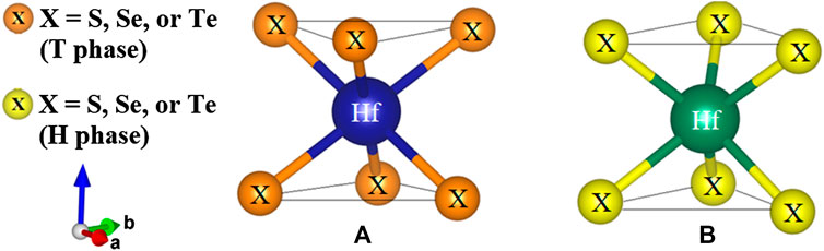
FIGURE 1. The local coordination of the two types (A) octahedral and (B) trigonal prismatic.
Monolayer TMDs have only two polymorphs, namely the T and H phases (Kolobov, 2016), depending on their hexagonal or trigonal prismatic coordination. In Figure 2, the crystal optimization for three compounds in the monolayer HfX2 family is performed with the top (xy plane) and side (yz plane) views. Hafnium (Hf) and two chalcogen atoms (X) form the X-Hf-X layered unit per unit cell, where the Hf atom is sandwiched between two X atoms referred to as a monolayer. In other words, each layer consists of three atomic planes that include one hafnium plane and two chalcogen planes through ionic-covalent interaction (see side view). From the top view, the spatial position of the chalcogen atoms is additionally filled with the light yellow triangles that show the different stacking in the two forms. The structural arrangements are constructed in the T and H phases with the period layer and trigonal symmetry being formulated by the octahedrally-coordinated stacking.
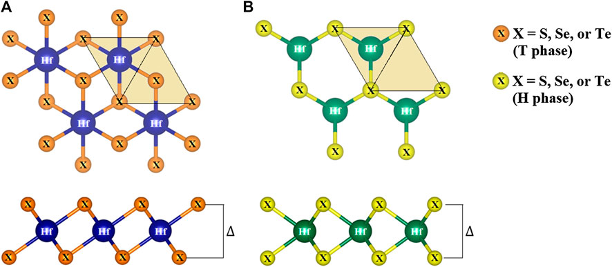
FIGURE 2. The top (xy plane) and side (yz plane) views of HfX2 (X = S, Se, or Te) in the (A) T phase and (B) H phase.
The formation energy is calculated using Eq. 1
where
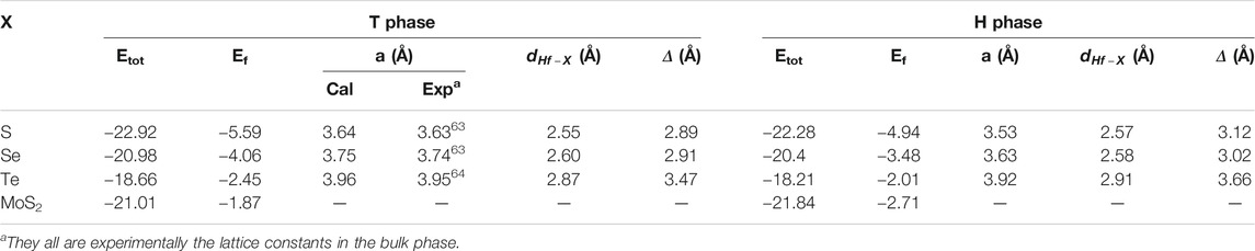
TABLE 1. Total energy (Etot, eV), formation energy (Ef, eV), the lattice constant (a, Å), chemical bonding between hafnium and chalcogen atoms (
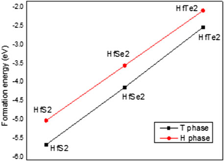
FIGURE 3. Formation energy of HfX2 in the T (black line) and H (red line) phases.
The calculated lattice constant, bond length, and buckling of monolayer T and H phases are also shown in Table 1. As shown in this table, the lattice constants of HfS2, HfSe2, and HfTe2 are, respectively, 3.64, 3.75, 3.96
Furthermore, monolayer HfX2 exists in a bucked form (
Electronic Properties
In the Brillouin zone, the electronic band structures have been calculated along with the high symmetry point Γ-M-K-Γ belonging to the hexagonal lattice. The system band gaps of monolayer HfX2 with the T and H phases are shown in Table 2. Both HfS2 and HfSe2 are semi-conducting with each material exhibiting distinct properties. HfS2 shows a middle-gap of 1.2 and 0.92 eV in the T and H phases, respectively. HfSe2 with these phases remains semi-conducting and belongs to a narrow-gap of 0.86 and 0.4 eV, respectively. In contrast, HfTe2 is semi-metallic. The values of approximately zero reveal it to be a gapless semimetal similar to graphene (Castro Neto et al., 2009). The experimental gaps of the monolayer T phase are also listed in Table 2. However, these values are smaller than the calculated band gaps, in which respectively exists a difference of approximate 0.6 and 0.3 eV for HfS2 and HfSe2. In this work, the band gaps are obtained from PBE functional, which notes that the approaches in calculating might cause the differences that are significant when comparing them to experimental values. Because most members of group IV (Ti, Zr, and Hf) TMDs are experimentally found in the T phase (Greenaway and Nitsche, 1965; Terashima and Imai, 1987), there is no recorded measurement for making a comparison for the H phase in this work.
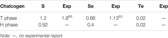
TABLE 2. The calculated band gap (Eg, eV) of monolayer HfX2 with the T and H phases and experimental values of the bandgap in the T phase monolayer.
The system band energy spectra of monolayer HfX2 are shown in Figure 4, which presents the atom dominances of hafnium and chalcogens. The left panel (Figures 4A–C) describes the system band of the T phase structures, and the right panel (Figures 4D–F) shows the system band of the H phase. All three materials share as a common feature that the valence band maximum (VBM) is located at Γ point (k = 0, 0, 0) and the conduction band minimum (CBM) is at M point (k = ½, 0, 0) of the high symmetry k-points in the T phase. While those of the H phase have a VBM between K and Γ point corresponding to the CBM is located between Γ and M point. The unoccupied conduction bands are asymmetric to the occupied valence bands about the Fermi level. Most energy bands have a strong dispersion relation, with the parabolic dispersion being exhibited in both the conduction and the valence bands. However, each material is predicted to have an unusual energy band. There are many distinguishing features between the T and H phases in the electronic band structures that are discussed below.
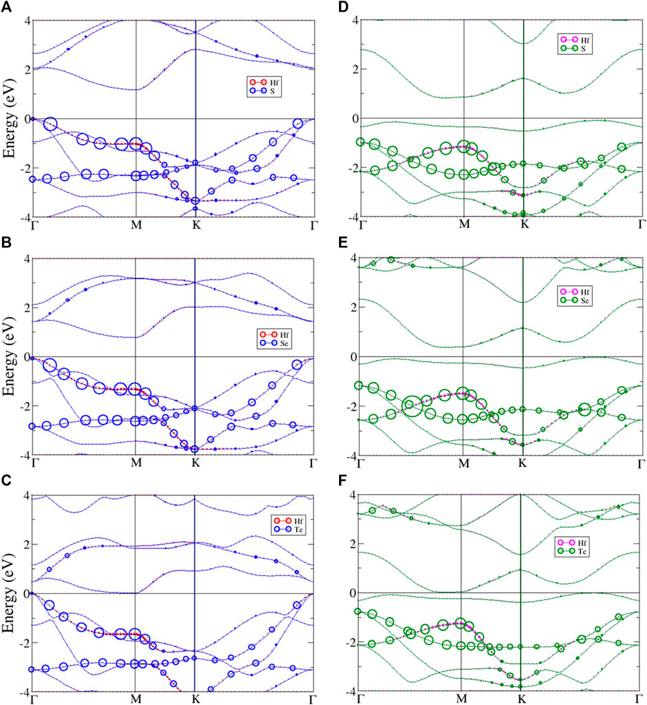
FIGURE 4. The band energy spectrum of monolayer (A) HfS2, (B) HfSe2, (C) HfTe2 with T phase, and (D) HfS2, (E) HfSe2, (F) HfTe2 with H phase. The red, magenta, blue, and green circles describe the atom dominant in the band for Hf and chalcogen atoms in T and H phase, respectively.
As previously mentioned, monolayer HfX2 (X = S, Se, or Te) are constructed with two phases that reveal distinct properties. The electronic bands of the T phase with atom dominance are described in Figures 4A–C (left panel). The red and blue circles respectively represent the hafnium and chalcogen atoms. They all show an indirect bandgap with the direction of the gap shifted from Γ point to M point. The occupied hole band is strongly asymmetric to the unoccupied electron band. The low-lying valence bands exhibit valleys between Γ and M point, as well as K and Γ point. The low-lying valence bands also change into parabolic bands. The parabolic dispersions have band-edge states at M point belonging to saddle points, which results in van Hove singularities (vHs). In Figure 4A, the
In order to compare with the T phase structures, the band energy spectra of the H phase are presented in Figures 4D–F (right panel). The green and magenta circles represent chalcogen and hafnium atoms. The occupied valence band and the unoccupied conduction band are asymmetric. Both HfS2 and HfSe2 still exhibit semiconducting with narrow-indirect gaps, but the direction is shifted from between K and Γ point to the point near M point. Similar to the T phase, HfTe2 remains semimetal with the same bandgap value (see Table 2). All the H phase structures exist in approximate flat bands near the Fermi level while the degeneracy lies below it, this leads to additional valleys in the low-lying valence bands. In Figure 4D, two
In general, the band energy spectra exhibit a lot of asymmetric peaks and few symmetric ones due to the parabolic form of energy bands. A pair of asymmetric peaks exists near the Fermi level that defines the indirect energy gaps. The bandgap opening is associated with the quantum confinement effect. Although all three materials are members of the same chalcogen group, HfS2, HfSe2, and HfTe2 are different in their low-lying peaks and degenerate with varying the stacking configuration between the two phases. Moreover, most van Hove singularities (vHs) come from the parabolic energy dispersions. The peaks near the Fermi level are found to arise from the band-edge states mainly. These peaks could be a signature feature unique to vHs.
The density of states (DOS) is shown in Figure 5 for the T and H phases, which directly reflect the main features of the band structures. DOS is ranged from −4 to 4 eV and shows a pair of asymmetric peaks centered at the Fermi level, which characterizes the energy gap. The large energy difference between the valence and conduction peaks obviously demonstrates the asymmetry of the two bands. These structures originate from linear bands, parabolic bands near saddle points, and initial band-edge states of the parabolic bands. In the T phase structures shown in Figure 5A, DOS exhibits a logarithmic divergence at middle energy and shoulder structures at deeper and higher energy. Partially flat energy is exhibited in the valence bands of all structures and in the conduction bands of HfSe2 and HfTe2, while shoulder structures evidently appear in the conduction band of HfS2. Moreover, the low DOS at the Fermi level illustrates the low free carrier density. In contrast, a linear energy dependence near the Fermi level is shown in the H phase structures (Figure 5B). The DOS of the H phase is much larger than that of the T phase at the Fermi level, indicating a higher free carrier density. At deeper and higher energy, DOS reveals peaks, as well as divergent and shoulder structures. Notice that the peak and shoulder structures correspond to the 3pz, 4pz, 5pz, and (3px,3py), (4px,4py), (5px,5py) of HfS2, HfSe2, and HfTe2, respectively, dominating energy bands as indicated in the orbital-projected DOS.
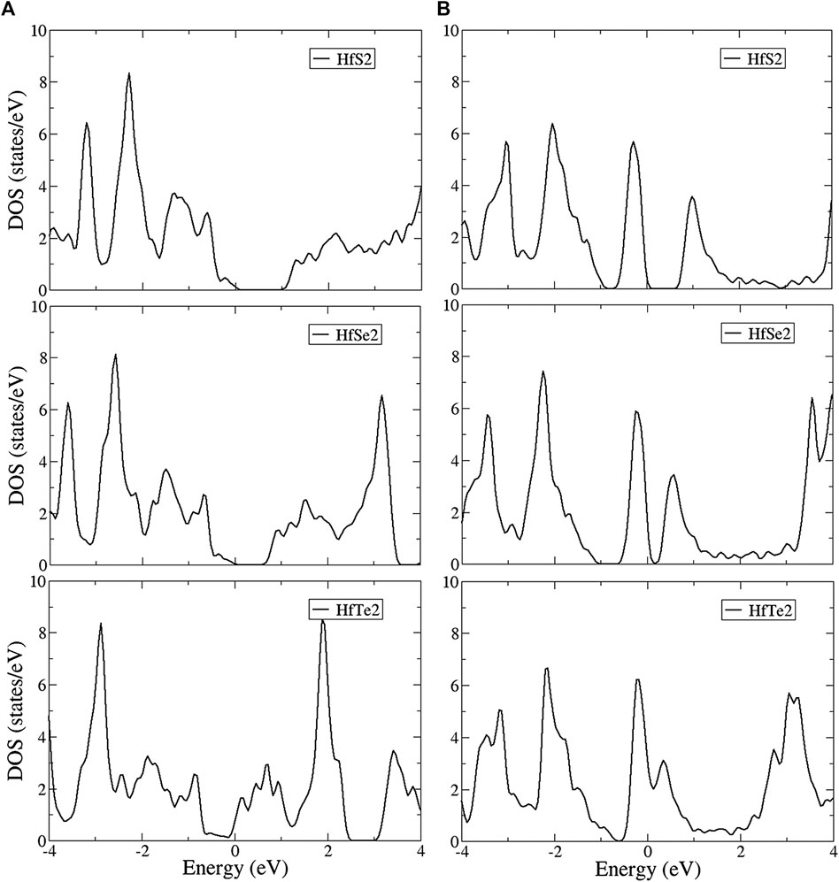
FIGURE 5. The density of states (DOS) in the (A) T and (B) H phase of monolayer HfX2.
To further verify the various chemical bondings and examine the curvature effect, the orbital-projected DOS could be used as described in Figures 6 and 7. The figures show the local density of states with multi-orbital hybridization in the T and H phases. They show that the main contributions are due to two orbitals of the hafnium and two orbitals of the chalcogens, corresponding to the s, d orbitals of hafnium, and the s, p orbitals of chalcogens. With the T phase structures, the local density of states with multi-hybridization is shown in Figure 6, presenting the dominance of the multi-orbital hafnium and chalcogen atoms. At high energy, hafnium atoms are dominated by 5
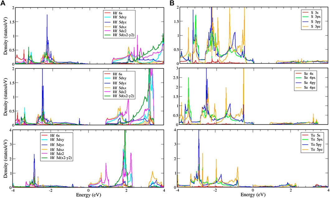
FIGURE 6. Local density of states (LDOS) of (A) hafnium and (B) chalcogen atoms with multi-orbital hybridization in the T phase.
Similar to the T phase, the H phase structures are shown in Figure 7 and indicate that the d-orbitals of hafnium and the p-orbitals of chalcogens, respectively, play essential roles in the conduction and valence bands. The 5
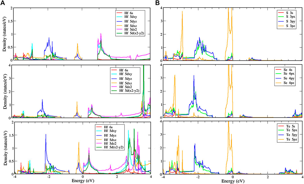
FIGURE 7. Local density of states (LDOS) of (A) hafnium and (B) chalcogen atoms with multi-orbital hybridization in the H phase.
Conclusion
The first-principles calculations are used to investigate the geometric and electronic properties of monolayer HfX2 (X = S, Se, or Te). Our calculated band structures in the T and H phases can modulate their properties. All structures exist with a sharp buckle that shows height fluctuations at equilibrium. The d-orbitals and p-orbitals of the hafnium and chalcogen atoms, respectively, take part in the chemical bondings of Hf-X. As reported, both HfS2 and HfSe2 are semiconductors with an indirect middle-gap and narrow-gap, respectively, while HfTe2 is a gapless semimetal. The energy gap trend suggests that the atomic species play a dominant role. A lot of asymmetric peaks and few symmetric ones due to the parabolic form are shown in the energy bands and density of states. The van Hove singularities mainly arise from the band-edge states in the DOS. The logarithmic divergence at middle energy and shoulder structures at lower and higher energy are exhibited in the DOS corresponding to the 3pz, 4pz, 5pz and (3px,3py), (4px,4py), (5px,5py) of HfS2, HfSe2 and HfTe2, respectively. In addition, these orbitals demonstrate multi-orbital hybridizations, as shown in the orbital-projected DOS. In summary, the electronic properties of the monolayer HfX2 family are mainly determined by their geometry, chemical bondings, and the orbitals hybridization.
Data Availability Statement
The original contributions presented in the study are included in the article/Supplementary Material, further inquiries can be directed to the corresponding author/s.
Author Contributions
TH: Conceptualization, Model building, Methodology, Software, Validation, Writing- Reviewing and Editing. DN: Model building, Data curation, Visualization, Original draft preparation. TN: Model building, Data curation, Visualization, Original draft. VD: Model building, Data curation, Visualization, Original draft preparation. NH: Model building, Data curation, Visualization, Original draft preparation. HP: Conceptualization, Model building, Methodology, Software, Validation, Reviewing and Editing, Supervision.
Conflict of Interest
The authors declare that the research was conducted in the absence of any commercial or financial relationships that could be construed as a potential conflict of interest.
Acknowledgments
This work was financially supported by the Hierarchical Green Energy Materials (Hi-GEM) Research Center, from The Featured Areas Research Center Program within the framework of the Higher Education Sprout Project by the Ministry of Education (MOE) and the Ministry of Science and Technology (MOST 108–3017-F-006–003) in Taiwan.
References
Abdulsalam, M., and Joubert, D. P. (2016). Optical spectrum and excitons in bulk and monolayer MX2 (M=Zr, Hf; X=S, Se). Phys. Status Solidi B 253 (4), 705–711. doi:10.1002/pssb.201552584
Aminalragia-Giamini, S., Marquez-Velasco, J., Tsipas, P., Tsoutsou, D., Renaud, G., and Dimoulas, A. (2016). Molecular beam epitaxy of thin HfTe2 semimetal films. 2D Mater. 4 (1). doi:10.1088/2053-1583/4/1/015001
Aretouli, K. E., Tsipas, P., Tsoutsou, D., Marquez-Velasco, J., Xenogiannopoulou, E., Giamini, S. A., et al. (2015). Two-dimensional semiconductor HfSe2 and MoSe2/HfSe2 van der Waals heterostructures by molecular beam epitaxy. Appl. Phys. Lett. 106 (14), 143105. doi:10.1063/1.4917422
Balandin, A. A., Ghosh, S., Bao, W., Calizo, I., Teweldebrhan, D., Miao, F., et al. (2008). Superior thermal conductivity of single-layer graphene. Nano Lett. 8 (3), 902–907. doi:10.1021/nl0731872
Bayliss, S. C., and Liang, W. Y. (1982). Symmetry dependence of optical transitions in group 4B transition metal dichalcogenides. J. Phys. C Solid State Phys. 15 (6), 1283–1296. doi:10.1088/0022-3719/15/6/021
Castro Neto, A. H., Guinea, F., Peres, N. M. R., Novoselov, K. S., and Geim, A. K. (2009). The electronic properties of graphene. Rev. Mod. Phys. 81 (1), 109–162. doi:10.1103/revmodphys.81.109
Cheng, C., Sun, J.-T., Chen, X.-R., and Meng, S. (2018). Hidden spin polarization in the 1 T -phase layered transition-metal dichalcogenides MX 2 ( M = Zr, Hf; X = S, Se, Te). Sci. Bull. 63 (2), 85–91. doi:10.1016/j.scib.2017.12.003
Chung, H. C., Lee, M. H., Chang, C. P., and Lin, M. F. (2011). Exploration of edge-dependent optical selection rules for graphene nanoribbons. Optic Express 19 (23), 23350–23363. doi:10.1364/oe.19.023350
Das, S., Robinson, J. A., Dubey, M., Terrones, H., and Terrones, M. (2015). Beyond graphene: progress in novel two-dimensional materials and van der Waals solids. Annu. Rev. Mater. Res. 45 (1), 1–27. doi:10.1146/annurev-matsci-070214-021034
Ding, G., Gao, G. Y., Huang, Z., Zhang, W., and Yao, K. (2016). Thermoelectric properties of monolayer MSe2 (M = Zr, Hf): low lattice thermal conductivity and a promising figure of merit. Nanotechnology 27 (37), 375703. doi:10.1088/0957-4484/27/37/375703
Ernzerhof, M., and Scuseria, G. E. (1999). Assessment of the Perdew-Burke-Ernzerhof exchange-correlation functional. J. Chem. Phys. 110 (11), 5029–5036. doi:10.1063/1.478401
Fiori, G., Bonaccorso, F., Iannaccone, G., Palacios, T., Neumaier, D., Seabaugh, A., et al. (2014). Electronics based on two-dimensional materials. Nat. Nanotechnol. 9 (10), 768–779. doi:10.1038/nnano.2014.207
Greenaway, D. L., and Nitsche, R. (1965). Preparation and optical properties of group IV-VI2 chalcogenides having the CdI2 structure. J. Phys. Chem. Solid. 26 (9), 1445–1458. doi:10.1016/0022-3697(65)90043-0
Guinea, F., Castro Neto, A. H., and Peres, N. M. R. (2006). Electronic states and Landau levels in graphene stacks. Phys. Rev. B 73 (24), 245426. doi:10.1103/physrevb.73.245426
He, J., Hummer, K., and Franchini, C. (2014). Stacking effects on the electronic and optical properties of bilayer transition metal dichalcogenides MoS2, MoSe2, WS2, and WSe2. Phys. Rev. B 89 (7), 075409. doi:10.1103/physrevb.89.075409
Hohenberg, P., and Kohn, W. (1964). Inhomogeneous electron gas. Phys. Rev. 136 (3B), B864–B871. doi:10.1103/physrev.136.b864
Hu, J. Q., Shi, X. H., Wu, S. Q., Ho, K. M., and Zhu, Z. Z. (2019). Dependence of electronic and optical properties of MoS2 multilayers on the interlayer coupling and Van Hove singularity. Nanoscale Res Lett. 14 (1), 288. doi:10.1186/s11671-019-3105-9
Huang, Y. K., Chen, S. C., Ho, Y. H., Lin, C. Y., and Lin, M. F. (2014). Feature-rich magnetic quantization in sliding bilayer graphenes. Sci. Rep. 4, 7509. doi:10.1038/srep07509
Hussain Reshak, A., and Auluck, S. (2005). Ab initio calculations of the electronic and optical properties of 1T-HfX2 compounds. Phys. B Condens. Matter. 363 (1–4), 25–31. doi:10.1016/j.physb.2005.02.030
Jiang, T., Liu, H., Huang, D., Zhang, S., Li, Y., Gong, X., et al. (2014). Valley and band structure engineering of folded MoS2 bilayers. Nat. Nanotechnol. 9 (10), 825–829. doi:10.1038/nnano.2014.176
Jiang, H. (2011). Structural and electronic properties of ZrX2 and HfX2 (X = S and Se) from first principles calculations. J. Chem. Phys. 134 (20), 204705. doi:10.1063/1.3594205
Kanazawa, T., Amemiya, T., Ishikawa, A., Upadhyaya, V., Tsuruta, K., Tanaka, T., et al. (2016). Few-layer HfS2 transistors. Sci. Rep. 6, 22277. doi:10.1038/srep22277
Kang, M., Rathi, S., Lee, I., Lim, D., Wang, J., Li, L., et al. (2015). Electrical characterization of multilayer HfSe2 field-effect transistors on SiO2 substrate. Appl. Phys. Lett. 106 (14), 143108. doi:10.1063/1.4917458
Kang, J., Zhang, L., and Wei, S.-H. (2016). A unified understanding of the thickness-dependent bandgap transition in hexagonal two-dimensional semiconductors. J. Phys. Chem. Lett. 7 (4), 597–602. doi:10.1021/acs.jpclett.5b02687
Kaul, A. B. (2014). Two-dimensional layered materials: structure, properties, and prospects for device applications. J. Mater. Res. 29 (3), 348–361. doi:10.1557/jmr.2014.6
Kim, S. J., Choi, K., Lee, B., Kim, Y., and Hong, B. H. (2015). Materials for flexible, stretchable electronics: graphene and 2D materials. Annu. Rev. Mater. Res. 45 (1), 63–84. doi:10.1146/annurev-matsci-070214-020901
Kreis, C., Werth, S., Adelung, R., Kipp, L., Skibowski, M., Krasovskii, E. E., et al. (2003). Valence and conduction band states of HfS2: from bulk to a single layer. Phys. Rev. B 68 (23), 235331. doi:10.1103/physrevb.68.235331
Kresse, G., and Hafner, J. (1993). Ab initiomolecular dynamics for liquid metals. Phys. Rev. B 47 (1), 558–561. doi:10.1103/physrevb.47.558
Kresse, G., and Joubert, D. (1999). From ultrasoft pseudopotentials to the projector augmented-wave method. Phys. Rev. B 59 (3), 1758–1775. doi:10.1103/physrevb.59.1758
Kumar, A., and Ahluwalia, P. K. (2012). Electronic structure of transition metal dichalcogenides monolayers 1H-MX2 (M = Mo, W; X = S, Se, Te) from ab-initio theory: new direct band gap semiconductors. Eur. Phys. J. B 85 (6), 186. doi:10.1140/epjb/e2012-30070-x
Lebègue, S., Björkman, T., Klintenberg, M., Nieminen, R. M., and Eriksson, O. (2013). Two-dimensional materials from data filtering and ab initio calculations. Phys. Rev. X 3 (3), 031002. doi:10.1103/physrevx.3.031002
Lin, C.-Y., Wu, J.-Y., Ou, Y.-J., Chiu, Y.-H., and Lin, M.-F. (2015). Magneto-electronic properties of multilayer graphenes. Phys. Chem. Chem. Phys. 17 (39), 26008–26035. doi:10.1039/c5cp05013hhttps://pubs.rsc.org/en/content/articlelanding/2015/CP/C5CP05013H#!divAbstract
Lin, Y.-K., Chen, R.-S., Chou, T.-C., Lee, Y.-H., Chen, Y.-F., Chen, K.-H., et al. (2016). Thickness-dependent binding energy shift in few-layer MoS2 grown by chemical vapor deposition. ACS Appl. Mater. Interfaces. 8 (34), 22637–22646. doi:10.1021/acsami.6b06615
Ma, R., Sheng, L., Shen, R., Liu, M., and Sheng, D. N. (2009). Quantum Hall effect in bilayer graphene: disorder effect and quantum phase transition. Phys. Rev. B 80 (20), 205101. doi:10.1103/physrevb.80.205101
Mangelsen, S., Naumov, P. G., Barkalov, O. I., Medvedev, S. A., Schnelle, W., Bobnar, M., et al. (2017). Large nonsaturating magnetoresistance and pressure-induced phase transition in the layered semimetal HfTe2. Phys. Rev. B 96 (20), 205148. doi:10.1103/physrevb.96.205148
McDonnell, S. J., and Wallace, R. M. (2016). Atomically-thin layered films for device applications based upon 2D TMDC materials. Thin Solid Films 616, 482–501. doi:10.1016/j.tsf.2016.08.068
Meng, L., Wang, Y., Zhang, L., Du, S., Wu, R., Li, L., et al. (2013). Buckled silicene formation on Ir(111). Nano Lett. 13 (2), 685–690. doi:10.1021/nl304347w
Mirabelli, G., McGeough, C., Schmidt, M., McCarthy, E. K., Monaghan, S., Povey, I. M., et al. (2016). Air sensitivity of MoS2, MoSe2, MoTe2, HfS2, and HfSe2. J. Appl. Phys. 120 (12), 125102. doi:10.1063/1.4963290
Mleczko, M. J., Zhang, C. F., Lee, H. R., Kuo, H. H., Magyari-Kope, B., Moore, R. G., et al. (2017). HfSe2 and ZrSe2: two-dimensional semiconductors with native high-κ oxides. Sci. Adv. 3 (8), 1700481. doi:10.1126/sciadv.1700481
Nakata, Y., Sugawara, K., Chainani, A., Yamauchi, K., Nakayama, K., Souma, S., et al. (2019). Dimensionality reduction and band quantization induced by potassium intercalation in 1T−HfTe2. Phys. Rev. Mater. 3 (7), 071001. doi:10.1103/physrevmaterials.3.071001
Nie, X.-R., Sun, B.-Q., Zhu, H., Zhang, M., Zhao, D.-H., Chen, L., et al. (2017). Impact of metal contacts on the performance of multilayer HfS2 field-effect transistors. ACS Appl. Mater. Interfaces. 9 (32), 26996–27003. doi:10.1021/acsami.7b06160
Novoselov, K. S., Mishchenko, A., Carvalho, A., and Castro Neto, A. H. (2016). 2D materials and van der Waals heterostructures Science 353 (6298), 9439. doi:10.1126/science.aac9439
Perdew, J. P., and Wang, Y. (2018). Erratum: accurate and simple analytic representation of the electron-gas correlation energy. Phys. Rev. B 98 (7), 079904. doi:10.1103/physrevb.98.079904
Perdew, J. P., Chevary, J. A., Vosko, S. H., Jackson, K. A., Pederson, M. R., Singh, D. J., et al. (1993). Erratum: atoms, molecules, solids, and surfaces: applications of the generalized gradient approximation for exchange and correlation. Phys. Rev. B 48 (7), 4978. doi:10.1103/physrevb.48.4978.2
Roubi, L., and Carlone, C. (1988). Resonance Raman spectrum ofHfS2 and ZrS2. Phys. Rev. B 37 (12), 6808–6812. doi:10.1103/physrevb.37.6808
Salavati, M. (2018). Electronic and mechanical responses of two-dimensional HfS2, HfSe2, ZrS2, and ZrSe2 from first-principles. Front. Struct. Civ. Eng. 13 (2), 486–494. doi:10.1007/s11709-018-0491-5
Setiyawati, I., Chiang, K.-R., Ho, H.-M., and Tang, Y.-H. (2019). Distinct electronic and transport properties between 1T-HfSe2 and 1T-PtSe2. Chin. J. Phys. 62, 151–160. doi:10.1016/j.cjph.2019.09.029
Sun, X., and Wang, Z. (2017). Ab initio study of adsorption and diffusion of lithium on transition metal dichalcogenide monolayers. Beilstein J. Nanotechnol. 8, 2711–2718. doi:10.3762/bjnano.8.270
Terashima, K., and Imai, I. (1987). Indirect absorption edge of ZrS2 and HfS2. Solid State Commun. 63 (4), 315–318. doi:10.1016/0038-1098(87)90916-1
Toh, R. J., Sofer, Z., and Pumera, M. (2016). Catalytic properties of group 4 transition metal dichalcogenides (MX2; M = Ti, Zr, Hf; X = S, Se, Te). J. Mater. Chem. 4 (47), 18322–18334. doi:10.1039/c6ta08089h
Traving, M., Seydel, T., Kipp, L., Skibowski, M., Starrost, F., Krasovskii, E. E., et al. (2001). Combined photoemission and inverse photoemission study of HfS2. Phys. Rev. B 63 (3), 035107. doi:10.1103/physrevb.63.035107
Tsai, H.-S., Liou, J.-W., Setiyawati, I., Chiang, K.-R., Chen, C.-W., Chi, C.-C., et al. (2018). Photoluminescence characteristics of multilayer HfSe2 synthesized on sapphire using ion implantation. Adv. Mater. Interfaces. 5 (8), 1701619. doi:10.1002/admi.201701619
Wu, N., Zhao, X., Ma, X., Xin, Q., Liu, X., Wang, T., et al. (2017). Strain effect on the electronic properties of 1T-HfS2 monolayer. Phys. E Low-dimens. Syst. Nanostruct. 93, 1–5. doi:10.1016/j.physe.2017.05.008
Xiao, D., Liu, G. B., Feng, W., Xu, X., and Yao, W. (2012). Coupled spin and valley physics in monolayers of MoS2 and other group-VI dichalcogenides. Phys. Rev. Lett. 108 (19), 196802. doi:10.1103/physrevlett.108.196802
Xu, K., Wang, Z., Wang, F., Huang, Y., Wang, F., Yin, L., et al. (2015). Ultrasensitive phototransistors based on few-layered HfS2. Adv. Mater. 27 (47), 7881–7887. doi:10.1002/adma.201503864
Yan, P., Gao, G.-y., Ding, G.-q., and Qin, D. (2019). Bilayer MSe2 (M = Zr, Hf) as promising two-dimensional thermoelectric materials: a first-principles study. RSC Adv. 9 (22), 12394–12403. doi:10.1039/c9ra00586b
Yin, L., Xu, K., Wen, Y., Wang, Z., Huang, Y., Wang, F., et al. (2016). Ultrafast and ultrasensitive phototransistors based on few-layered HfSe2. Appl. Phys. Lett. 109 (21), 213105. doi:10.1063/1.4968808
Yue, R., Barton, A. T., Zhu, H., Azcatl, A., Pena, L. F., Wang, J., et al. (2015). HfSe2 thin films: 2D transition metal dichalcogenides grown by molecular beam epitaxy. ACS Nano. 9 (1), 474–480. doi:10.1021/nn5056496
Yun, W. S., Han, S. W., Hong, S. C., Kim, I. G., and Lee, J. D. (2012). Thickness and strain effects on electronic structures of transition metal dichalcogenides: 2H-MX2 semiconductors (M = Mo, W; X = S, Se, Te). Phys. Rev. B 85 (3), 033305. doi:10.1103/physrevb.85.033305
Zeng, H., and Cui, X. (2015). An optical spectroscopic study on two-dimensional group-VI transition metal dichalcogenides. Chem. Soc. Rev. 44 (9), 2629–2642. doi:10.1039/c4cs00265b
Zeng, H., Dai, J., Yao, W., Xiao, D., and Cui, X. (2012). Valley polarization in MoS2 monolayers by optical pumping. Nat. Nanotechnol. 7 (8), 490–493. doi:10.1038/nnano.2012.95
Zhang, L., Zhang, Y., Camacho, J., Khodas, M., and Zaliznyak, I. (2011). The experimental observation of quantum Hall effect of l=3 chiral quasiparticles in trilayer graphene. Nat. Phys. 7 (12), 953–957. doi:10.1038/nphys2104
Zhang, W, Huang, Z., Zhang, W., and Li, Y. (2014). Two-dimensional semiconductors with possible high room temperature mobility. Nano Res. 7 (12), 1731–1737. doi:10.1007/s12274-014-0532-x
Zhao, Q., Guo, Y., Si, K., Ren, Z, Bai, J., and Xu, X. (2017). Elastic, electronic, and dielectric properties of bulk and monolayer ZrS2, ZrSe2, HfS2, HfSe2 from van der Waals density‐functional theory. Phys. Status Solidi (B) 254 (9), 1700033. doi:10.1002/pssb.201700033
Keywords: first-principles, two-dimensional materials, transition metal dichalcogenides, HfX2 (X = S, Se, or Te), geometry, multi-orbital hybridization, electronic properties
Citation: Huynh TMD, Nguyen DK, Nguyen TDH, Dien VK, Pham HD and Lin M-F (2021) Geometric and Electronic Properties of Monolayer HfX2 (X = S, Se, or Te): A First-Principles Calculation. Front. Mater. 7:569756. doi: 10.3389/fmats.2020.569756
Received: 05 June 2020; Accepted: 29 September 2020;
Published: 01 March 2021.
Edited by:
Gang Zhang, Institute of High Performance Computing (IHPC), SingaporeReviewed by:
Junfeng Gao, Dalian University of Technology, ChinaHo Won Jang, Seoul National University, South Korea
Copyright © 2021 Huynh, Nguyen, Nguyen, Dien, Pham and Lin. This is an open-access article distributed under the terms of the Creative Commons Attribution License (CC BY). The use, distribution or reproduction in other forums is permitted, provided the original author(s) and the copyright owner(s) are credited and that the original publication in this journal is cited, in accordance with accepted academic practice. No use, distribution or reproduction is permitted which does not comply with these terms.
*Correspondence: Ming-Fa Lin, bWZsaW5AbWFpbC5uY2t1LmVkdS50dw==; Hai Duong Pham, cGhhbWR1b25nNDc3QGdtYWlsLmNvbQ==