 Yuhang Xu
 Fei Lu1*
- 1School of Information Science and Engineering, Shandong University, Qingdao, China
- 2Department of Radiation Oncology, Qilu Hospital of Shandong University, Jinan, China
For this study, a dozen-micron-scale four to seven layers of graphene were synthesized directly onto Lithium Niobate (LiNbO3, LN) by carbon implantation in a nickel covered LiNbO3 film. The 1.52E16 ions·cm−2 carbon ions of 80 keV were implanted into the nickel film to a depth of 100 nm, which is close to the interface between the nickel film and the LiNbO3. The implanted carbon atoms dissolved in nickel at an elevated temperature and diffused towards the interface between the nickel film and LiNbO3 during annealing. After the nickel film fell off, the graphene material was found by Raman spectroscopy and confirmed by the Atomic Force Microscope topographic image. This implantation combined with patterned metal film suggests possibilities for engineering two-dimensional graphene with special confinement. It also provides a valuable and novel way for integrating graphene-wafer structure for other available substrate wafer in microelectronics and photonics devices.
Introduction
Graphene has received increasing attention since the successful preparation of it in 2004 (Novoselov et al., 2004). Single-layer graphene is a two-dimensional honeycomb lattice structure composed of a single layer of carbon atoms, and each carbon atom is bonded to the surrounding carbon atoms through SP2 hybridization (Xu et al., 2013). This structure has excellent conductivity. The electron mobility of graphene is higher than that of carbon nanotubes or silicon crystals. At room temperature, it can reach 15000 cm2 (V−1·s−1), while the resistivity is as low as about 10–6 Ω cm (Chen, 2015). Graphene also has high transmittance to light. The graphene monolayer absorbs only 2.3% of visible light, that is, it has a high transmittance (97.7%) in a wide spectral range from visible to infrared (Zhu et al., 2010). Graphene also has exceptionable mechanical properties, due to an elastic modulus of 1.0 TPa, its inherent tensile strength of 130 GPa and a two-dimensional ultimate plane strength of 42 N·m−1 (Lee et al., 2008). As a material, graphene has excellent thermal conductivity (up to 5500 W (m−1k−1)) and high specific surface area (up to 2630 m2g−1) (Wang et al., 2017). Due to this special structure, outstanding thermal conductivity and mechanical properties, graphene has aroused great interest from the scientific community in recent years (Geim and Novoselov, 2007; Geim, 2009; Ma et al., 2018; Martín-García et al., 2018), and is expected to trigger a revolution in the field of modern optoelectronic technology.
The preparation and application of graphene have been explored in many studies over the past decade. Common preparation technologies include micro-mechanical peeling (Novoselov et al., 2004), pyrolysis of silicon carbide (Juang et al., 2009), Chemical Vapor Deposition(CVD) (Li et al., 2009) and reduction of graphene oxide (Yin et al., 2011). The CVD method allows for the production of wafer-scale graphene layers, which has become the most popular technology. In recent years, a physical process has been proposed to synthesize graphene that involves the ion implantation of carbon into metal film and post-implantation annealing. Compared with a CVD method, ion implantation is a non-thermal equilibrium process, and has no requirements in terms of the carbon solubility of the material being implanted. The ability to control the number of layers of synthetic graphene may be possible by precisely adjusting the implantation dose (Garaj et al., 2010; Zhang et al., 2013). At present, transition metal nickel or copper are usually used to form graphene by carbon implantation (Garaj et al., 2010; Baraton et al., 2011a; Mun et al., 2012; Wang et al., 2013; Zhang et al., 2013; Lee et al., 2014; Kim et al., 2015; Wang et al., 2016). As the solubility of carbon in nickel decreases significantly with the decline of temperature, the carbon dissolved in nickel at high temperature will become saturated with the decrease of annealing temperature, and with the progress of thermal diffusion, they will eventually spread to the surface of the metal to form a single-layer or multi-layer graphene (Lander et al., 1952; Berry, 1973; Baraton et al., 2011b).
The application of graphene must be based on the graphene/substrate structure, and a lot of research has been conducted in recent years, but these studies are mainly focused on graphene/Si(SiO2) structure (Yoon et al., 2009; Garaj et al., 2010; Baraton et al., 2011b; Wang et al., 2011; Kumari et al., 2014; Lee et al., 2014; Dong et al., 2016; Onishi et al., 2017; Zuppella et al., 2017; Faggio et al., 2019; Ma et al., 2020). Few studies have focused on graphene/optical crystal, but among those that have , the combination of graphene and Lithium Niobate (LiNbO3, LN) is one of the most promising structures for development. LN is a nearly all-around artificial crystal, it has ferroelectric, piezoelectric, pyroelectric, photovoltaic, photoelastic, photorefractive and other properties, and has a wide range of applications unmatched by other crystals, known as “silicon materials in the optical field” (Graca et al., 2012; Boes et al., 2018; He et al., 2019; Kong et al., 2019). Its combination with graphene may have an impact on the quantum properties of two-dimensional materials, resulting in new photoelectric properties, which will inevitably have a wide range of potential applications (Jin et al., 2013; Baeumer et al., 2015; Salas et al., 2017a; Salas et al., 2018). For example, some studies have theoretically explored the interfacial properties of the combination of graphene and LN crystals (Wang et al., 2015; Salas et al., 2017b). One typical example is the modulation of carrier doping of graphene via LN polarization properties. The results show that by adjusting the carrier doping in graphene in the graphene/LN structure, the formation and propagation of surface plasmons polaritons can be controlled.
Previously, graphene bonding to substrates was mostly based on the graphene transfer method. However, the resulting graphene/LN or Si (SiO2) structures often suffer from graphene defects caused by the transfer process which leads to additional graphene degradation. Therefore, it’s necessary to study the direct synthesis of graphene/LN structure. The formation of graphene on the LN surface using direct carbon implantation of LN has been reported in our previous study (Liu et al., 2019), which found that the carbon implanted into the LN can accumulate on the crystal surface by out-diffusion at a moderate temperature and eventually form graphene. The carbon diffusion pathways, on the other hand, is related to the distribution of damage of LN lattice induced by carbon implantation. However, in this experiment only turbostratic graphene was demonstrated on the LN surface. LN has a complex structure, the solubility and diffusion behavior of carbon in LN is still unclear.
In this article, we report the direct synthesis of graphene on the surface of LN by annealing the post-carbon-implantation sample consisting of surface transition metal film and LN substrate. In the present experiment the carbon ions were implanted into the metal film covering the surface of the crystal rather than into the LN itself. This approch used the nickel as a catalyst, and graphene growth was based on the large solubility change of carbon ions in nickel films at different temperatures. Graphene was synthesized at the interface of nickel/LN, and the realization of immediate contact between graphene and LN omits the conventional intermediate process of graphene transfer. Our research provides a new method of preparation for applying graphene on substrates without transfer. Importantly, it provides a new approch that enables the direct synthesis of graphene that can create specific shapes and sizes on any substrates, which is often emphasized in photoelectric crystals such as LN.
Materials and Methods
A schematic diagram of the experimental method used in this study is shown in Figure 1. The substrate was Z-cut 10 × 10 × 0.5 mm3 bulk LN with Chemical Mechanical Polishing on one 10 × 10 mm2 surface for the following nickel coating. First, a layer of nickel foil is deposited on this surface as an overlay, and then the deposited sample is implanted with carbon ion. During the annealing process, the implanted carbon moves to the interface between the nickel foil and LN crystal. Ideally, a few layers of graphene will be formed, and finally, the nickel foil is removed to gain the graphene/LN structure.
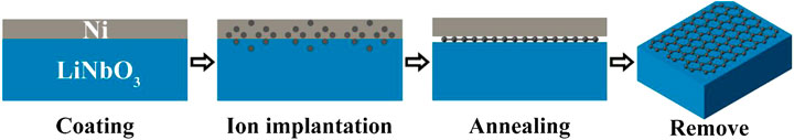
FIGURE 1. A schematic diagram of the steps of the experiment.
The thin layer of nickel was deposited on the surface of LN by resistance heating evaporation. As shown in Figure 2A, the thickness of the nickel foil measured by Atomic Force Microscope (AFM) is around 134 nm. The dose of carbon ion implantation we used is 1.52E16 ions·cm−2, which is selected to match the carbon content of four-layer graphene, and the ion energy of 80 keV ensures that the implanted carbons distribute near the interface between the nickel foil and LN crystal. Figure 2B shows the carbon ion distribution along the depth profiles simulated by Stopping and Range of Ion in Matter (SRIM) in the nickel/LN sample. According to SRIM simulation, the peak of carbon concentration is at roughly 100 nm below the surface of nickel film and is close to the interface between nickel and LN. The variation of the carbon concentration with the depth of implantation approximately follows the Gaussian distribution and the nickel film holds more than 80% in all implanted carbon. Subsequently, the as-implanted sample was annealed in the furnace. It was first heated to 900 °C at a rate of 10 °C·min−1, an kept at this temperature for 30 min, then allowed to naturally cooled to room temperature. The entire annealing process was carried out in N2 ambient, with a gas flow rate of 100 sccm (standard-state cubic centimeter per minute) and pressure of 6E4Pa.
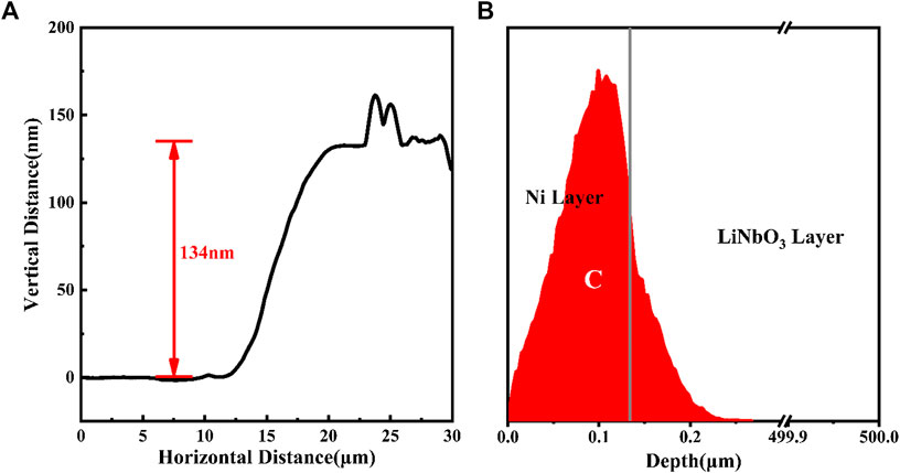
FIGURE 2. (A) AFM height profiles along the straight line from uncoated notch to the coated area (B) Structural schematic diagram of the coated bulk LN crystal with the distribution of carbon ions along with the depth profiles, simulated by SRIM.
Results and Discussions
The sample was first observed with an optical microscope, the images of the sample before and after annealing were shown in Figures 3A,B, respectively. Wrinkles appeared on the surface of the annealed sample. This phenomenon occurs on the one hand, because of the poor adhesion between the deposited metal film and the LN substrate, and on the other, due to the different thermal expansion properties of the two materials. Figure 3C shows the enlarged two-dimensional AFM image of the wrinkles on the surface of the sample, and Figures 3D, E are the respective height profiles along the solid red line one and line two marked in Figure 3C, respectively. As revealed by these images, the average height of the folds is around 0.7–1.8 μm and the width is about 10 μm. To determine the cause of the wrinkles, another two kinds of samples (one without carbon ion implantation and the other with carbon ion implantation) of the same coating treatment were annealed under the same conditions. It was found that both samples had similar wrinkles. This shows that the occurrence of wrinkles on the surface of this sample depends on the surface nickel film and the LN substrate themselves, and has nothing to do with carbon ion implantation.
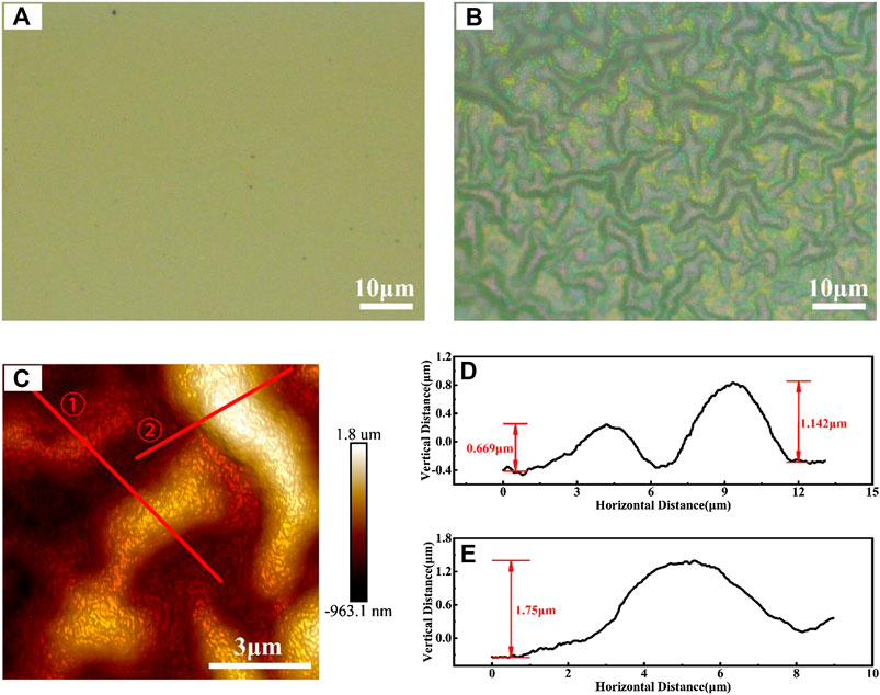
FIGURE 3. (A, B) The optical microscope images of the surface of the bulk LN crystal with nickel film before (A) and after annealing (B) (C) AFM topographic image of the wrinkles, and (D)–(E) AFM height profiles along the solid red line one and line two in (C).
No information of carbon material was detected by Raman spectroscopy on the upper surface of the nickel film, which excludes the case where carbon is precipitated from the nickel surface. The existence of wrinkles makes the nickel film easy to peel off. After the nickel film fell off, the LN surface was observed with a scanning electron microscope (SEM). A strong carbon signal was detected, indicating that the implanted carbon was mainly deposited at the interface between nickel and LN after annealing. Some carbon atoms converge into large clusters, which are distributed on the surface of LN. Figures 4A, B show the SEM image and its Energy Dispersive Spectrometer (EDS) mapping distribution of carbon from one of the clusters respectively. The highlights of the carbon distribution seen in Figure 4B fit well with the material distribution profile, and the Raman Spectra with the excitation wavelength at 532 nm from three, positions marked in Figure 4A, also confirmed that the aggregated carbon exhibits an amorphous structure. As can be seen in Figure 4C, the Raman curves at three locations show similar profiles. The D and G peaks are merged into one peak, while the 2D peak shows a very gentle and wide span distribution. This characteristic indicates that the carbon here is amorphous carbon with poor crystallinity (Shimodaira and Masui, 2002; Kaniyoor and Ramaprabhu, 2012; Sathish-Kumar et al., 2012). Figures 4D,E indicate the AFM of this cluster and its height profiles along marked red solid lines respectively. The height of the carbon material is about 1 μm, which is consistent with the height of the bulge in the wrinkled nickel film in Figure 3, which is around 0.7–1.8 μm. It is reasonable to suppose that the amorphous carbon material gathered and developed in wrinkled bumps and that the bulged nickel film provides space for holding these carbon materials. Improving the deposit of nickel film and its adhesion to LN is one of the key factors for ensuring the uniformity of carbon distribution.
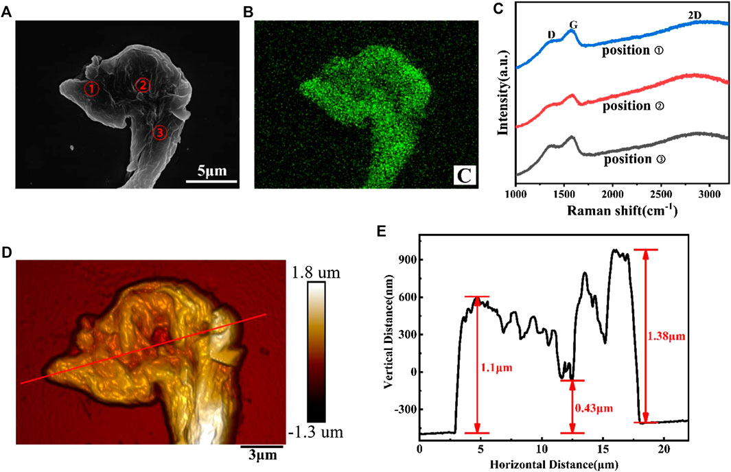
FIGURE 4. (A) SEM image of the amorphous carbon material on LN (B) EDS mapping for C element in the region shown in (A) (C) Raman Spectra of three positions shown in (A) (D) AFM topographic image of the amorphous carbon material, and (E) AFM height profiles along the solid red line in (D).
We also found other forms of carbon structures on the surface of the LN, as shown in Figure 5A is the SEM image from part of the sample surface, and Figures 5(B)–(D) are the corresponding EDS mapping diagrams of Nb, C and O elements at the same area, respectively. It can be seen that the elements Nb and O, which come from the LN substrate, are distributed uniformly. While the distribution of element C seen in Figure 5C is consistent with the morphology of Figure 5A, indicating that the spots on the surface are carbon materials. Subsequently, Raman spectra with 532 nm excitation wavelength for the five marked positions one to five in Figures 5A,C, which correspond to exactly the same positions, were obtained, as shown in Figure 6.
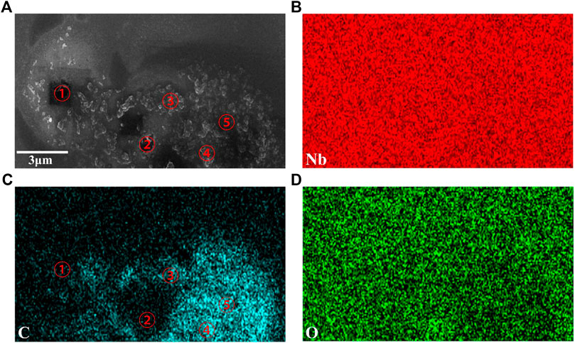
FIGURE 5. (A) SEM image of graphene on LN (B)–(D) EDS mapping for Nb, C, and O elements in the region shown in (A).
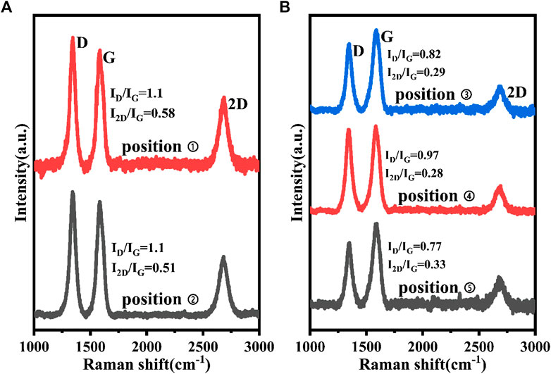
FIGURE 6. Raman Spectra of (A) positions one and two, (B) positions three, four, and five in Figure 5.
The Raman spectra at positions one and two are similar, revealing spectral features and uniquely characteristic of graphene films: a G peak (1,580 cm−1) associated with sp2 carbon bond stretching, a D peak (1,345 cm−1) arising from symmetry-breaking features, such as graphene defects and domain boundaries, and a 2D peak (2,690 cm−1) sensitive to the graphene inter layer interactions (Garaj et al., 2010;Han et al., 2011; Mun et al., 2012; Lee et al., 2014). The ratios of ID to IG (a measure of disorder) and I2D to IG (determined by the number of stacked graphene layers) are very similar, and are often used as the main parameters to judge the structural defects and the number of layers of graphene (Garaj et al., 2010; Lee et al., 2014). The corresponding ratio values of 1.1 and ∼0.5 indicate that the number of graphene layers is four to seven layers (Yu et al., 2008; Wang et al., 2013; Zhang et al., 2013). At the same time, the ratios of ID to IG are also higher at positions one and two, indicating that the graphene is defective. The graphene we obtained had many defects, including the mixing of multiple structures, graphene fragmentation, folding and structural distortion. This is the main reason for the larger ID/IG ratio. The spectra at positions three to five are shown in Figure 6B, where three distinct Raman peaks of D, G, and 2D are also visible. However, the ratio of I2D to IG is much lower than those of positions one and two, which is only around 0.3, suggesting that the graphene here could be a stacked multilayer structure. This result indicates that the carbon materials at these positions have the structural characteristics of turbostratic graphene (Garlow et al., 2016; Liu et al., 2019). Turbostratic graphene is a multilayer structure with a disordered arrangement, and its properties are significantly different from the structured two-dimensional multilayer graphene. Since our research focus is to obtain a two-dimensional multilayer graphene structure on LN, the results of positions one and two are of particular note.
The SEM image around position one in Figure 5 is shown in Figure 7A, some layered structures were observed. Subsequently, we conducted AFM scanning around positions one and two in Figure 5, and the results are shown in Figures 7B–E. A depression in the dark spot can be found at the test center point due to the loss of graphene caused by multiple Raman spectroscopy measurements. The height difference between the depression and the surrounding area represents the thickness of the multilayer graphene here. Figures 7B,C are the AFM topographic image around locations one and two, and Figures 7D,E are the profiles along the three different solid yellow lines in Figures 7B,C, respectively. It can be seen that there is a downward hollow in Figures 7D,E, which is the edge depression of a few layers of graphene. Although the three height change curves of each set in the figure are slightly different, on average, the depth of the depression at position one and two are about 46 and 70 nm respectively. These results are consistent with the estimations from our Raman results, an I2D/IG ratio of 0.58 in position one representing four to six layers of graphene, while 0.51 in position two represents five to seven layers of graphene. They also all correspond to the thickness values of four to six layers and five to seven layers multilayer graphene measured with AFM in references (Wu et al., 2009; Lee et al., 2014).
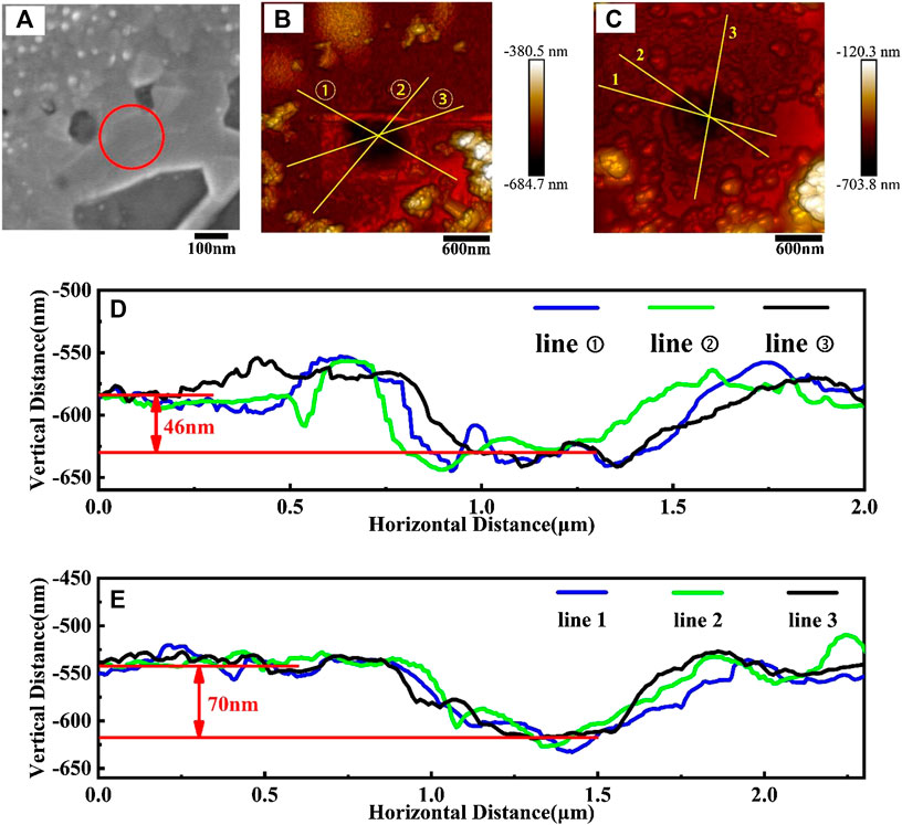
FIGURE 7. (A) SEM image around position one in Figure 5, (B,C) are the AFM topographic image around locations one and two in Figure 5, (D,E) are the profiles along the three different solid yellow lines in figure (B) and figure (C).
The direct two-dimensional synthesis of graphene on the surface of LN by carbon implantation has been proved to be feasible in our experimental scheme, although there are still many areas that need improvement. The current experimental results show that as a host for carbon ions, the quality of the nickel film and the uniform adhesion between the nickel and the LN substrate are important factors that affect the formation and structure of graphene. One of the improvements to the current experimental method is to use magnetron sputtering instead of vacuum evaporation to grow nickel thin films, which will increase the uniformity of nickel and the adhesion to the substrate.
The control of the annealing process is also an important factor, because proper annealing may reduce the thermal mismatch between the two materials during expansion and contraction. Thermal annealing is the only way to form graphene through carbon precipitation. The sample is firstly annealed at high temperature to accommodate more carbon and then cooled down so that the carbon becomes saturated in nickel as the temperature decreases, and the graphene is formed when the carbon overflows to the interface between nickel and LN with thermal diffusion. Since the diffusion property of carbon depends on several variables, such as the concentration gradient of carbon, the distance from carbon to the nickel/LN interface, the temperature range and temperature rise and fall speed, and ambient gas, etc., make the determination of annealing conditions particularly difficult. Therefore, the establishment of appropriate annealing conditions requires repeated adjustments, improvements, and measurements, which are currently being carried out in our research.
Conclusion
In our experiment, the 1.52E16 ions·cm−2 carbon ions of 80 keV were implanted to the nickel/LN substrate, which consists of an LN crystal covered with a layer of 134 nm thick nickel metal film. The implantation depth was 100 nm according to simulation by SRIM, which is close to the interface between the nickel film and LN. During post-implanted annealing, the sample was heated to 900°C and held for 30 min, then cooled down naturally in situ. After annealing, the nickel film on the surface of LN was wrinkled and easy to fall off. This can be attributed to the weak bonding between the nickel film and LN substrate and their mismatch thermal expansion coefficients. No signal of carbon material was detected by Raman spectroscopy from the upper surface of the nickel film, which excludes a result of carbon precipitation from the upper surface of the nickel film. After the nickel film fell off, two kinds of carbon structures were found on the surface of the LN substrate by SEM, EDS, and Raman spectroscopy. First, amorphous carbon with poor crystallinity gathered and developed under the bulge of the wrinkled nickel film. Second, the graphene structure with an uneven number of layers mixed with turbostratic graphene and four to seven layers of two-dimensional graphene, as confirmed by AFM topographic image. The direct synthesis of two-dimensional graphene on the surface of LN was proved in our experimental scheme, which draws on the experiences of predecessors in the synthesis of graphene by carbon ion implantation of nickel, but our experiment omitted the process of film transfer. In particular, implantation combined with patterned metal film suggests the possibility of engineering two-dimensional graphene with special confinement, which is often emphasized in photoelectric crystals such as LN. The flexibility of photolithography technology in the metal pattern may makes it achievable to potentially form an air-graphene-wafer system with special nanostructure, such as graphene nano-disk. Direct synthesis of graphene with patterned and even distribution on the LN is our next research goal, and further experiments are in progress.
Data Availability Statement
The raw data supporting the conclusions of this article will be made available by the authors, without undue reservation.
Author Contributions
YX, and FL: conceptualization, data curation, formal analysis, methodology, and writing - review and editing. FL: funding acquisition, supervision and validation. YX, FL, and KL: investigation. YX, KL, and CM: project administration. YX: visualization and writing - original draft.
Funding
This study was funded by the National Natural Science Foundation of China (Grant Number 61975094).
Conflict of Interest
The authors declare that the research was conducted in the absence of any commercial or financial relationships that could be construed as a potential conflict of interest.
Acknowledgments
We would like to thank Dr Mingsheng Xu, School of Microelectronics, Shandong University for the use of his equipment.
References
Baeumer, C., Saldana-Greco, D., Martirez, J. M. P., Rappe, A. M., Shim, M., and Martin, L. W. (2015). Ferroelectrically driven spatial carrier density modulation in graphene. Nat. Commun. 6, 6136. doi:10.1038/ncomms7136
Baraton, L., He, Z. B., Lee, C. S., Cojocaru, C. S., Châtelet, M., Maurice, J.-L., et al. (2011a). On the mechanisms of precipitation of graphene on nickel thin films. Epl 96, 46003. doi:10.1209/0295-5075/96/46003
Baraton, L., He, Z., Lee, C. S., Maurice, J.-L., Cojocaru, C. S., Gourgues-Lorenzon, A.-F., et al. (2011b). Synthesis of few-layered graphene by ion implantation of carbon in nickel thin films. Nanotechnology 22, 085601. doi:10.1088/0957-4484/22/8/085601
Berry, B. S. (1973). Diffusion of carbon in nickel. J. Appl. Phys. 44, 3792–3793. doi:10.1063/1.1662846
Boes, A., Corcoran, B., Chang, L., Bowers, J., and Mitchell, A. (2018). Status and potential of lithium niobate on insulator (LNOI) for photonic integrated circuits. Laser Photon. Rev. 12, 1700256. doi:10.1002/lpor.201700256
Chen, C.-M. (2015). Surface chemistry and macroscopic assembly of graphene for application in energy storage. PhD thesis. Beijing (China): University of Chinese Academy of Sciences.
Dong, T., Sparkes, M., Durkan, C., and O‘Neill, W. (2016). Evaluating femtosecond laser ablation of graphene on SiO2/Si substrate. J. Laser Appl. 28, 022202. doi:10.2351/1.4944510
Faggio, G., Gnisci, A., Messina, G., Lisi, N., Capasso, A., Lee, G. H., et al. (2019). Carbon dots dispersed on graphene/SiO2/Si: a morphological study. Phys. Status Solidi. 216, 1800559. doi:10.1002/pssa.201800559
Garaj, S., Hubbard, W., and Golovchenko, J. A. (2010). Graphene synthesis by ion implantation. Appl. Phys. Lett. 97, 183103. doi:10.1063/1.3507287
Garlow, J. A., Barrett, L. K., Wu, L., Kisslinger, K., Zhu, Y., and Pulecio, J. F. (2016). Large-area growth of turbostratic graphene on Ni(111) via physical vapor deposition. Sci. Rep. 6, 19804. doi:10.1038/srep19804
Geim, A. K. (2009). Graphene: status and prospects. Science 324, 1530–1534. doi:10.1126/science.1158877
Geim, A. K., and Novoselov, K. S. (2007). The rise of graphene. Nat. Mater. 6, 183–191. doi:10.1038/nmat1849
Graca, M. P. F., Prezas, P. R., Costa, M. M., and Valente, M. A. (2012). Structural and dielectric characterization of LiNbO3 nano-size powders obtained by Pechini method. J. Sol. Gel Sci. Technol. 64, 78–85. doi:10.1007/s10971-012-2829-0
Han, G. H., Güneş, F., Bae, J. J., Kim, E. S., Chae, S. J., Shin, H.-J., et al. (2011). Influence of copper morphology in forming nucleation seeds for graphene growth. Nano Lett. 11, 4144–4148. doi:10.1021/nl201980p
He, M., Xu, M., Ren, Y., Jian, J., Ruan, Z., Xu, Y., et al. (2019). High-performance hybrid silicon and lithium niobate Mach-Zehnder modulators for 100 Gbit s−1 and beyond. Nat. Photon. 13, 359–364. doi:10.1038/s41566-019-0378-6
Jin, D., Kumar, A., Hung Fung, K., Xu, J., and Fang, N. X. (2013). Terahertz plasmonics in ferroelectric-gated graphene. Appl. Phys. Lett. 102, 201118. doi:10.1063/1.4807762
Juang, Z.-Y., Wu, C.-Y., Lo, C.-W., Chen, W.-Y., Huang, C.-F., Hwang, J.-C., et al. (2009). Synthesis of graphene on silicon carbide substrates at low temperature. Carbon 47, 2026–2031. doi:10.1016/j.carbon.2009.03.051
Kaniyoor, A., and Ramaprabhu, S. (2012). A Raman spectroscopic investigation of graphite oxide derived graphene. AIP Adv. 2, 032183. doi:10.1063/1.4756995
Kim, J., Lee, G., and Kim, J. (2015). Wafer-scale synthesis of multi-layer graphene by high-temperature carbon ion implantation. Appl. Phys. Lett. 107, 033104. doi:10.1063/1.4926605
Kong, Y., Bo, F., Wang, W., Zheng, D., Liu, H., Zhang, G., et al. (2019). Recent progress in lithium niobate: optical damage, defect simulation, and on-chip devices. Adv. Mater. 32, 1806452. doi:10.1002/adma.201806452
Kumari, A., Prasad, N., Bhatnagar, P. K., Mathur, P. C., Yadav, A. K., Tomy, C. V., et al. (2014). Electrical transport properties of polycrystalline CVD graphene on SiO2/Si substrate. Diam. Relat. Mater. 45, 28–33. doi:10.1016/j.diamond.2014.03.003
Lander, J. J., Kern, H. E., and Beach, A. L. (1952). Solubility and diffusion coefficient of carbon in nickel: reaction rates of nickel-carbon alloys with barium oxide. J. Appl. Phys. 23, 1305–1309. doi:10.1063/1.1702064
Lee, C., Wei, X., Kysar, J. W., and Hone, J. (2008). Measurement of the elastic properties and intrinsic strength of monolayer graphene. Science 321, 385–388. doi:10.1126/science.1157996
Lee, J. S., Jang, C. W., Kim, J. M., Shin, D. H., Kim, S., Choi, S.-H., et al. (2014). Graphene synthesis by C implantation into Cu foils. Carbon 66, 267–271. doi:10.1016/j.carbon.2013.08.066
Li, X., Cai, W., An, J., Kim, S., Nah, J., Yang, D., et al. (2009). Large-area synthesis of high-quality and uniform graphene films on copper foils. Science 324, 1312–1314. doi:10.1126/science.1171245
Liu, K., Lu, F., Li, K., Xu, Y., and Ma, C. (2019). Synthesis of turbostratic graphene by direct carbon ions implantation on LiNbO3. Appl. Surf. Sci. 493, 1255–1259. doi:10.1016/j.apsusc.2019.07.105
Ma, R.-S., Ma, J., Yan, J., Wu, L., Guo, W., Wang, S., et al. (2020). Wrinkle-induced highly conductive channels in graphene on SiO2/Si substrates. Nanoscale 12, 12038. doi:10.1039/d0nr01406k
Ma, X., Liu, Y., Liu, H., Zhang, L., Xu, B., and Xiao, F. (2018). Fabrication of novel slurry containing graphene oxide-modified microencapsulated phase change material for direct absorption solar collector. Sol. Energy Mater. Sol. Cell. 188, 73–80. doi:10.1016/j.solmat.2018.08.021
Martín-García, B., Bi, Y., Prato, M., Spirito, D., Krahne, R., Konstantatos, G., et al. (2018). Reduction of moisture sensitivity of PbS quantum dot solar cells by incorporation of reduced graphene oxide. Sol. Energy Mater. Sol. Cell. 183, 1–7. doi:10.1016/j.solmat.2018.04.005
Mun, J. H., Lim, S. K., and Cho, B. J. (2012). Local growth of graphene by ion implantation of carbon in a nickel thin film followed by rapid thermal annealing. J. Electrochem. Soc. 159, G89–G92. doi:10.1149/2.059206jes
Novoselov, K. S., Geim, A. K., Morozov, S. V., Jiang, D., Zhang, Y., Dubonos, S. V., et al. (2004). Electric field effect in atomically thin carbon films. Science 306, 666–669. doi:10.1126/science.1102896
Onishi, K., Kirimoto, K., and Sun, Y. (2017). Coupling behaviors of graphene/SiO2/Si structure with external electric field. AIP Adv. 7, 025113. doi:10.1063/1.4975150
Salas, O., Garcés, E., Castillo, F. L., and Magaña, L. F. (2017a). Absorption and reflectivity of the lithium niobate surface masked with a graphene layer. AIP Adv. 7, 015305. doi:10.1063/1.4974745
Salas, O., Garcés, E., Castillo, F. L., and Magaña, L. F. (2017b). Changes in the reflectivity of a lithium niobate crystal decorated with a graphene layer. J. Phys.: Conf. Ser. 792, 012069. doi:10.1088/1742-6596/792/1/012069
Salas, O., Garces, E., and Magana, L. (2018). Optical absorption and reflectivity of a molecular cluster of lithium niobate adsorbed on a graphene layer. Crystals 8, 208. doi:10.3390/cryst8050208
Sathish-Kumar, K., Vázquez-Huerta, G., Rodríguez-Castellanos, A., Poggi-Varaldo, H. M., and Solorza-Feria, O. (2012). Microwave assisted synthesis and characterizations of decorated activated carbon. Int. J. Electrochem. Sci. 7, 5484–5494.
Shimodaira, N., and Masui, A. (2002). Raman spectroscopic investigations of activated carbon materials. J. Appl. Phys. 92, 902–909. doi:10.1063/1.1487434
Wang, G., Ding, G., Zhu, Y., Chen, D., Ye, L., Zheng, L., et al. (2013). Growth of controlled thickness graphene by ion implantation for field-effect transistor. Mater. Lett. 107, 170–173. doi:10.1016/j.matlet.2013.06.013
Wang, H., Zhao, H., Hu, G., Li, S., Su, H., and Zhang, J. (2015). Graphene based surface plasmon polariton modulator controlled by ferroelectric domains in lithium niobate. Sci. Rep. 5, 18258. doi:10.1038/srep18258
Wang, J., Ma, F., and Sun, M. (2017). Graphene, hexagonal boron nitride, and their heterostructures: properties and applications. RSC Adv. 7, 16801–16822. doi:10.1039/c7ra00260b
Wang, X., Berke, K., Rudawski, N. G., Venkatachalam, D. K., Elliman, R. G., Fridmann, J., et al. (2016). Synthesis of graphene and graphene nanostructures by ion implantation and pulsed laser annealing. J. Appl. Phys. 120, 025105. doi:10.1063/1.4955137
Wang, X., Xu, J.-B., Wang, C., Du, J., and Xie, W. (2011). High-performance graphene devices on SiO2/Si substrate modified by highly ordered self-assembled monolayers. Adv. Mater. 23, 2464–2468. doi:10.1002/adma.201100476
Wu, Z.-S., Ren, W., Gao, L., Liu, B., Jiang, C., and Cheng, H.-M. (2009). Synthesis of high-quality graphene with a pre-determined number of layers. Carbon 47, 493–499. doi:10.1016/j.carbon.2008.10.031
Xu, M., Liang, T., Shi, M., and Chen, H. (2013). Graphene-like two-dimensional materials. Chem. Rev. 113, 3766–3798. doi:10.1021/cr300263a
Yin, K., Li, H., Xia, Y., Bi, H., Sun, J., Liu, Z., et al. (2011). Thermodynamic and kinetic analysis of lowtemperature thermal reduction of graphene oxide. Nano-Micro Lett. 3, 51–55. doi:10.1007/BF03353652
Yoon, D., Moon, H., Son, Y.-W., Choi, J. S., Park, B. H., Cha, Y. H., et al. (2009). Interference effect on Raman spectrum of graphene onSiO2/Si. Phys. Rev. B 80, 125422. doi:10.1103/PhysRevB.80.125422
Yu, Q., Lian, J., Siriponglert, S., Li, H., Chen, Y. P., and Pei, S.-S. (2008). Graphene segregated on Ni surfaces and transferred to insulators. Appl. Phys. Lett. 93, 113103. doi:10.1063/1.2982585
Zhang, R., Wang, Z. S., Zhang, Z. D., Dai, Z. G., Wang, L. L., Li, H., et al. (2013). Direct graphene synthesis on SiO2/Si substrate by ion implantation. Appl. Phys. Lett. 102, 193102. doi:10.1063/1.4804982
Zhu, Y., Murali, S., Cai, W., Li, X., Suk, J. W., Potts, J. R., et al. (2010). Graphene and graphene oxide: synthesis, properties, and applications. Adv. Mater. 22, 3906–3924. doi:10.1002/adma.201001068
Keywords: graphene, direct synthesis, lithium niobate substrate, carbon ion implantation, nickel film, annealing
Citation: Xu Y, Lu F, Liu K and Ma C (2020) Direct Graphene Synthesis on Lithium Niobate Substrate by Carbon Ion Implantation. Front. Mater. 7:572280. doi: 10.3389/fmats.2020.572280
Received: 13 June 2020; Accepted: 28 August 2020;
Published: 10 November 2020.
Edited by:
Ming Xu, Huazhong University of Science and Technology, ChinaReviewed by:
Jiangtao Di, Suzhou Institute of Nano-Tech and Nano-Bionics (CAS), ChinaHoracio Javier Salavagione, Consejo Superior de Investigaciones Científicas (CSIC), Spain
Copyright © 2020 Xu, Lu, Liu and Ma. This is an open-access article distributed under the terms of the Creative Commons Attribution License (CC BY). The use, distribution or reproduction in other forums is permitted, provided the original author(s) and the copyright owner(s) are credited and that the original publication in this journal is cited, in accordance with accepted academic practice. No use, distribution or reproduction is permitted which does not comply with these terms.
*Correspondence: Fei Lu, bHVmZWlAc2R1LmVkdS5jbg==