 Jiapeng Xu1
 Lichuan Jin
 Zhimin Liao
 Qi Wang
- 1State Key Laboratory of Electronic Thin Films and Integrated Devices, University of Electronic Science and Technology of China, Chengdu, China
- 2Beijing Key Laboratory of Quantum Devices, Peking University, Beijing, China
- 3Collaborative Innovation Center of Quantum Matter, Peking University, Beijing, China
- 4Faculty of Physics, University of Vienna, Vienna, Austria
With the continuous miniaturization of electronic devices and the increasing speed of their operation, solving a series of technical issues caused by high power consumption has reached an unprecedented level of difficulty. Fortunately, magnons (the quanta of spin waves), which are the collective precession of spins in quantum magnetic materials, making it possible to replace the role of electrons in modern information applications. In the process of information transmission, nano-sized spin-wave devices do not transport any physical particles; therefore, the corresponding power consumption is extremely low. This review focuses on the emerging developments of the spin-wave materials, tunable effects, and functional devices applications. In the materials front, we summarize the magnetic properties and preparation characteristics of typical insulating single-crystalline garnet films or metallic alloy films, the development of new spin-wave material system is also introduced. Afterward, we introduce the emerging electric control of spin-wave effects originating from the interface transitions, physical or chemical, among these films including, voltage-controlled magnetic anisotropy, magneto-ionic transport, electric spin-torque, and magnon-torque. In the functional devices front, we summarize and elaborate on the low dispassion information processing devices and sensors that are realized based on spin waves.
Introduction
With the rapid development of science and technology, the revolution of electronic information technology has greatly changed our lives just within the course of few decades. The technological achievements of this decade have subverted people's imagination a century ago. First invented in 1959, the integrated circuits have developed rapidly over the past 60 years. One of the key factors is Moore’s Law (Moore, 1965). In the past few decades, people have always regarded Moore's Law as the core driving force for the development of the electronic information industry. Nevertheless, since 2005, one of the key elements of maintaining Moore's Law, the miniaturization of semiconductor devices, has been significantly slowed down due to intrinsic physical constraints (Theis and Wong, 2017). This brings the imminent question, how long does Moore’s Law sustain? If Moore’s Law comes to an end, what would be the future of the integrated circuit industry? Three approaches are proposed in the related literature as the key plans to perpetuate the development of the integrated circuit industry, namely “more Moore” (Li, 2012), “more than Moore” (Graef, 2011; Salah, 2017) and “beyond CMOS” (Hutchby et al., 2002; Bernstein et al., 2010; Nikonov and Young, 2013; Nikonov and Young, 2015; Pan and Naeemi, 2017).
Spin-wave devices based on magnetic materials are a new type of devices proposed under “beyond COMS” concept to replace the traditional charge transport devices (Rana and Otani, 2019). Spin is an intrinsic particles’ property described in quantum mechanics, and spin waves are collective precession generated by the interaction of electron spins in metals, semiconductors, and insulators (Kruglyak et al., 2010). Spin-wave devices use wave amplitude, phase, and frequency as the carrier of information transmission and processing. The process of spin-wave propagation is only based on electron spin interactions, thus no physical particle transportation is involved. This results in extremely low power consumption by the spin-wave devices compared to the conventional CMOS devices (Kajiwara et al., 2010; Khitun et al., 2010). In addition, spin-wave sensors have a higher level of thermal stability and the innovative principle of magnetism provides them with unique advantages. Comparing with the conventional sensors, these provide the spin-wave sensors with a higher sensitivity, thermal stability, and lower cost (Goto et al., 2015; Matatagui et al., 2017).
Spin waves usually propagate in the waveguides made of magnetic thin films or strips. The spin-wave dispersion (the relationship between the spin-wave frequency f and the wave number k) depends on various parameters, such as the waveguide geometry (Chumak et al., 2014), Oersted field induced by the electric current (Rousseau et al., 2015) and spin-wave material properties (Qin et al., 2018), etc. Among these parameters, the magnetic material determines the basic performance of the device. Therefore, the choice of material is a key factor in the application of the spin-wave devices.
Single-crystal yttrium iron garnet (YIG) has a small Gilbert damping constant, a narrow ferromagnetic resonance linewidth, and other highlights (Dubs et al., 2017). Nevertheless, its saturation magnetization is rather small which limits its spin-wave frequency. Other spin-wave alloy materials, such as permalloy, CoFeB, and Heusler alloy have a higher saturation magnetization and Curie temperature (Chumak et al., 2017), but their Gilbert damping constants are one to two orders of magnitude larger than YIG. Materials with such a high Gilbert damping constant are not conducive to the propagation and practical application of spin waves. The preparation of spin-wave thin films needs to consider both the film quality and film thickness, but these two indicators are usually opposed to each other. To pursue better spin-wave characteristics and new magnetic physical phenomena, the exploring of new materials aims at emerging fields such as antiferromagnetic materials (Nishitani et al., 2010), YIG modification (Sharma and Kuanr, 2018) and topological magnon insulators (Wang et al., 2018c). The structure design of spin-wave materials is mainly focused on magnonic crystals (Nikitov et al., 2001; Chumak et al., 2008; Krawczyk and Grundler, 2014). At the same time, the new interface effects found in magnetic heterostructures provide innovative means for spin-wave manipulation.
Various magnetoelectric effects, including voltage-controlled magnetic anisotropy (VCMA) (Dieny and Chshiev, 2017), magneto-ionic transport (Tan et al., 2019), electric spin-torque (Madami et al., 2011; Divinskiy et al., 2018) and magnon-torque (Wang et al., 2019), are capable of improving the spin-wave manipulation efficiency while effectively reduce the power consumption during the process. Therefore, magnetoelectric effects enable the development of all-voltage-controlled spin-wave devices with extremely low power consumption.
Spin-wave functional devices have also been developed steadily based on spin-wave materials and the related effects and are becoming a mature technology. The basic manipulation processes required by spin-wave logic devices such as spin-wave phase shift (Wang et al., 2018b), signal division (Heussner et al., 2017), and channeling (Wagner et al., 2016) are also achieved. Spin-wave sensors have also attracted increasing attention due to their high level of thermal stability (Goto et al., 2015), accuracy (Matatagui et al., 2017).
The above-mentioned recent developments enable spin waves to find their roles in modern information applications. In this paper, an application chain of the spin-wave information technology is constructed. The application chain is built upon the spin-wave materials, their novel interface effects, and spin-wave functional devices. We start from the magnetic properties and preparation characteristics of typical spin-wave materials. Then we introduce the latest developments including recent exploration of new (e.g., antiferromagnetic spin-wave materials, modified YIG and topological magnon insulators), and structurally designed materials (e.g., magnonic crystals). We then summarize the origins, mechanisms, and applications of novel magnetoelectric effects in magnetic heterostructures, including VCMA, magneto-ionic transport, electric spin-torque, and magnon-torque. After reviewing the spin-wave materials and interface effects, we further introduce the internal principles and outstanding advantages of the latest spin-wave functional devices from the perspective of information processing and sensing. Finally, we conclude the current status of spin-wave technology, and further provide some insights on the future development trends in this research area.
Quantum Spin-Wave Theory and Materials
Basic Theory of Spin-Wave
The existence of several major energy terms in micromagnetic theory provides an explanation for the concept of effective field in the process of spin-wave propagation. These energy terms can be considered as Zeeman energy, exchange energy, magnetocrystalline anisotropy energy and demagnetizing energy.
Under the static magnetic field
We consider only the Heisenberg interaction, so that the exchange energy is given by
J is the nearest neighbor exchange parameter,
Where
The effective field can be obtained
where
Under the semi-classical approximation, the relationship between magnetic moment μ and angular momentum L is as follows:
In a ferromagnet, the magnetization M is the magnetic moment per unit volume, and Landau-Lifeshitz (LL) equation can be obtained by replacing μ
In the above equation, if the magnetization vector M is not parallel to the effective field Heff, the magnetic moment μ will keep precessing around the direction of Heff, which obviously does not meet the physical law. To solve this problem, T. Gilbert introduced the damping term, and the magnetic moment will be parallel to the effective field direction gradually under the damping action. Landau-Lifshitz and Gilbert (LLG) equation is obtained, where α is the dimensionless damping factor
The spin-wave is the non-uniform precession of the magnetic moments, and the adjacent magnetic moments are not parallel. For a standard ellipsoid, the effective field can be expressed by
where
where
Equation 2.12 represents the relationship between the spin-wave frequency ω and the wave vector k, which is also called the spin-wave dispersion relationship.
It is worth mentioning that, in addition to solving the governing equation of spin-wave propagation using the classical LLG equation, another method using first-principles is also very successful (see reference (Tancogne-Dejean et al., 2020)). Tancogne-Dejean et al. obtained systematic dynamical properties through the time-dependent Kohn−Sham equations in real time, which reveals the transverse magnetic excitation spectrum of the magnet, and provides an important reference to analyze magnonic excitation within the first-principles framework.
Magnetic Properties of Typical Spin-Wave Materials
We have witnessed an unprecedented progress in the discovery of new materials, structures and effects during the last 100 years. The exquisite blueprints drawn by the scientists and researchers and materialized by the industry fundamentally affected and changed our day-to-day life. Similarly, spin-wave materials have been rapidly developed by the introduction of spin-wave functional devices. During the last few decades, in-depth investigations have shown that magnetic materials, such as YIG (Dubs et al., 2017), permalloy (Michelini et al., 2002), CoFeB (Conca et al., 2013) and Heusler alloy (Kubota et al., 2009) provide clear advantages as spin-wave carriers.
Chumak et al. (2017) summarized the magnetization parameters and spin-wave characteristics of the above-mentioned four typical spin-wave materials, and concluded that the spin-wave materials should have four basic requirements: a) a small-value Gilbert damping constant that ensures that propagation of spin waves without excessive dissipation; b) a high saturation magnetization that ensures sufficient spin-wave frequency and group velocity; c) a high-value Curie temperature that provides thermal stability; and d) ease of processing. Gilbert damping constant, the intrinsic parameter of spin-wave materials, determines the group velocity of spin waves, and the product of spin-wave group velocity and lifetime is the mean free path of spin waves. Since the mean free path represents the transmission capacity of spin waves in the waveguide, Gilbert damping constant is one of the most important parameters of spin-wave materials. The saturation magnetization of spin-wave materials also determines the propagating frequency and group velocity. Furthermore, Curie temperature represents the critical point for ferromagnetic/ferrimagnetic materials to transform into paramagnetic materials, which is the key factor to evaluate the thermal stability of spin-wave electronic devices.
As it is seen in Table 1, Gilbert damping constant of single-crystal YIG thin film (μm-thick) is in order of 10–5. The lifetime of spin waves in μm-thick YIG thin films is in order of hundreds of nanoseconds, and the mean free path is in order of thousands of microns. This set of characteristics is unmatched by any other materials. This is because YIG has a weak spin-orbit interaction, which results in a weaker magnon-phonon coupling than other magnetic materials. Therefore, YIG demonstrates an extremely low magnetic loss and Gilbert damping constant (Dubs et al., 2017). Note that permalloy and CoFeB are amorphous, and Heusler alloy is single crystal. Compared to YIG, spin-wave alloy materials still have a big gap in spin-wave propagation characteristics, but they generally have a higher saturation magnetization and Curie temperature. Therefore, the spin waves have a higher frequency in alloy materials, and metal-based spin-wave devices are more stable at high temperature. It should be also noted that permalloy is known for its high permeability, low coercivity, and low magnetic anisotropy (Chin, 1971; Michelini et al., 2002), and is an important part of spin valve devices (Tanoue and Tabuchi, 2001). Heusler alloy with semi-metallic properties have a very large spin polarization effect (Hillebrands and Felser, 2006) due to the energy gap in the up and down spin channel at its Fermi level, which results in generating fully spin-polarized conduction electrons (Kubota et al., 2009).
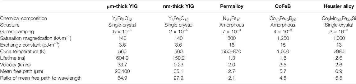
TABLE 1. Magnetic parameters and spin-wave characteristics of four typical spin-wave materials (Chumak et al., 2017) (licensed under CC BY 3.0).
Preparation Characteristics of Typical Spin-Wave Materials
Table 2 summarizes the preparation characteristics of the thin films made of the above four spin-wave materials, including the main preparation technologies, substrate materials, and main preparation parameters. Magnetron sputtering is relatively common among various preparation technologies. This is because magnetron sputtering is easy to adjust and capable of sputtering the high-melting-point target materials made of different metals, alloys, and oxides (Kelly and Arnell, 2000). In addition, permalloy thin films prepared by electrochemical deposition have the most prominent feature of rapid growth (Zubar et al., 2018). Among the thin film parameters, thickness and surface roughness are considered as the key factors for preparing micro-nano spin-wave electronic devices.
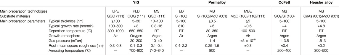
TABLE 2. The preparation characteristics of the thin films made of four typical spin-wave materials. Main preparation technologies include liquid phase epitaxy (LPE), pulsed laser deposition (PLD), magnetron sputtering (MS), electrochemical deposition (ED), and molecular beam epitaxy (MBE). Room temperature is abbreviated as RT.
In general, thinning thickness is one of the main development trends in spin-wave materials. However, the magnetization dynamic characteristics of YIG ultra-thin films with nanometer-level thickness are not constant and their spin-wave attenuation length, group velocity, Gilbert damping, and other spin-wave characteristics may decline. The lowest Gilbert damping constant for such films is around 2 × 10⁻⁴ (Onbasli et al., 2014). Although YIG ultra-thin provides great advantages over other type of materials, it is far from YIG bulk materials. This is mainly due to the internal structure, composition phase and surface morphology of the films. Therefore, the preparation technology of nanometer-thick spin-wave films remains to be further explored.
YIG thin films are generally grown on gadolinium gallium garnet (GGG) substrates with (111) orientation. The main preparation techniques include liquid phase epitaxy (LPE), pulsed laser deposition (PLD), and magnetron sputtering (MS). The details of LPE has been developed in 1970s and fuses solute and flux with a proper composition at a high temperature to form saturated melt for film preparation. The supercooling effect is then achieved by cooling within a large temperature range. Due to the supercooled precipitation of solute, YIG thin films with the same lattice constant as the substrate then grow on the substrate at a constant temperature. Although the preparation process is complex and the preparation cost is high, it is still one of the best choices for the preparation of μm-thick YIG films (Levinstein et al., 1971; Dubs et al., 2017). YIG films prepared by LPE method are relatively thick, and the typical root mean square (RMS) surface roughness value is maintained at a high level, between 0.3–0.8 nm. Another preparation technology, PLD, is recently considered as the mainstream choice of YIG ultrathin films. The basic preparation process of PLD is using a high-energy pulsed laser to ionizes the specific target. The plasma plume generated is then deposited and then nucleated on the surface of the GGG substrate. The PLD requires oxygen atmosphere, and its main advantage is the ability to obtain a more accurate stoichiometric ratio than that of other preparation technologies. This enables preparation of YIG ultra-thin films with thickness as low as 5 nm, and up to the standard surface roughness and magnetic properties (Sun et al., 2012; d’Allivy Kelly et al., 2013). MS can also be used to prepare YIG thin films, but the obtained Gilbert damping constant is generally about three times larger than that of PLD. This is because the sputtering parameters have an important influence on the microstructure of the films (Liu et al., 2014). For instance, a higher annealing temperature and a longer annealing time tend to aggravate the diffusion effect of atoms at the interface.
The preparation techniques of permalloy materials are mainly based on electrochemical deposition (ED), magnetron sputtering (MS), and molecular beam epitaxy (MBE). The most prominent characteristics of ED is the capability of achieving an extremely fast film deposition rate at the room temperature. However, its higher surface roughness has a negative impact on the film quality (Lamrani et al., 2015; Zubar et al., 2018), and using the electrolyte solution raises concerns on potential environmental pollution. The thin film prepared by MS under vacuum has a more uniform composition. Furthermore, permalloy is easier to deposit comparing to other materials. Therefore, the thickness of permalloy prepared by MS can be as low as 1 nm (Michelini et al., 2002). For the MBE, the substrate temperature required is relatively low and the film deposition rate is also small. As the entire deposition process is precisely controlled, the pressure of preparation is as low as 5 × 10⁻⁶ mTorr (Tanaka et al., 2010; Ohtake et al., 2011). A crucial disadvantage of the MBE is its high production cost which is due to its long preparation cycle, and high environmental pollution management costs.
The most common preparation technology for CoFeB and Heusler alloy is MS. MS was used in the preparation of pure aluminum films and alloy films as early as 1970s (McLeod and Hartsough, 1977), and was widely used in the preparation of various high-quality films in the past decades (Kelly and Arnell, 2000). The gas pressure during magnetron sputtering deposition of amorphous CoFeB thin films has a great influence on the magnetization dynamics (Xu et al., 2012). The sputtered Heusler alloy has the best spin-wave properties among the three alloys. The gilbert damping constant in Heusler alloy thin film can reach to 3 × 10⁻³ (Trudel et al., 2010), and the maximum spin-wave attenuation length is around 16.7 μm (Sebastian et al., 2012), which is closely related to the unique semi-metallic property of Heusler alloy (Kubota et al., 2009).
Development of New Spin-Wave Material Systems
Antiferromagnetic Spin-Wave Materials
Antiferromagnets are highly magnetically ordered materials with periodic and symmetrical magnetic moments. In contrast with ferromagnetic materials, the magnetic moments of adjacent atoms in antiferromagnetic materials are antiparallel and two sets of opposite magnetic sublattices are closely coupled (Kittel, 1951). Therefore, below Neel temperature, antiferromagnetic materials macroscopically appear to be nonmagnetic. This special antiferromagnetic structure results in no net magnetism in the ground state. Such a characteristic result in increased robustness to the external stray magnetic fields. This further causes easily magnetic excitation at terahertz frequencies under the interaction of its internal strong exchange coupling and other external disturbances, e.g., laser irradiation (Nishitani et al., 2010). In addition, the maximum driven velocity of antiferromagnetic domain wall is several orders of magnitude larger than that of ferromagnetic domain wall (Shiino et al., 2016). Although some studies have explained the antiferromagnetic ordering of CaFe2As2 based on the interaction between spin waves and magnetic exchange (see, e.g., Zhao et al., 2009), the antiferromagnetic properties need further investigations.
Recently, researchers paid a lot of attention to antiferromagnetic spin waves and magnons. By applying other technologies, antiferromagnetic materials (especially NiO) have shown unique advantages in magnon excitation and spin-wave manipulation at high frequency and high speed. Nishitani et al. (2010) realized THz spin-wave excitation of antiferromagnetic single-crystal NiO under femtosecond laser irradiation and showed that Raman scattering is the likely mechanism behind this phenomenon. The relativistic kinematics of antiferromagnets explain that by increasing the domain wall velocity to the spin-wave group velocity, the domain wall is capable to emit THz spin waves (Shiino et al., 2016). Furthermore, it is shown that the energy can be transferred to the magnon mode by optical excitation. This has been proved through experiments by inverse Faraday effect and inverse Cotton-Mouton effect, where the excitation efficiency of the latter is about three orders of magnitude higher than that of the former (Tzschaschel et al., 2017).
High frequency magnon excitation in antiferromagnetic materials shows remarkable characteristics. Further, using antiferromagnetic ordering for quick controlling of the spin and polarization degrees of freedom in spin waves provides great technical advantages. For instance, by controlling the spin degree of freedom in a terahertz pulsed electric field at the femtosecond timescale, Kampfrath et al. (2011) demonstrated switching of coherent spin waves in antiferromagnetic materials at the frequency of 1 THz. Further, Lan et al. (2017) used domain walls as spin-wave polarizers and retarders by using the polarization degree of freedom of the spin waves. This was mainly due to capability of antiferromagnets to accommodate both left-circular and right-circular polarized spin-wave modes.
Antiferromagnetic materials also create the smallest spin-wave waveguide on record. For the first time, Patil et al. (2016) reported propagation of 43 THz spin waves in NiO nanorods with a length of 700 nm. Such a small size is explained based on the unique antiferromagnetism and geometric characteristics of NiO nanorods, and based on the fact that magneto-optical Faraday effect is the key factor in the process of spin-wave detection. Traditional Brillouin scattering spectroscopy can only be used to detect and observe spin waves with a few microns of wavelength.
Modification of Yttrium Iron Garnet
Modification of YIG is usually referred to the preparation of new materials by doping YIG (Rare-Earth-Doped Yttrium Iron Garnets, R: YIG) or replacing Y (Rare-Earth Iron Garnets, RIG) with other rare Earth elements. Modified YIG materials provide outstanding advantages in terms of spin-wave performance and magneto-optical properties.
Table 3 summarizes the characteristics of the modified YIG made by doping or substituting YIG with Eu, Lu, Tm, and other rare Earth elements. Comparing the modified YIG in Table 3, with those of pure YIG materials in Table 1, it is seen that the spin-wave damping property in modified YIG is not improved, and the Gilbert damping constant in pure YIG is the smallest (5 × 10⁻⁵). In Ce: YIG, the Gilbert damping constant of Y2.85C0.15Fe5O12 is 2.8 × 10⁻³ (Sharma and Kuanr, 2018). With the increase of Ce content, the Gilbert damping constant of Y2C1Fe5O12 increases to the order of 10–2 (Kehlberger et al., 2015), and the similar situation occurs in La: YIG (Sharma and Kuanr, 2018; Jin et al., 2019). If Y is completely replaced by other rare Earth elements (e.g., Eu, Lu and Tm), the Gilbert damping constant in RIG is around 10–2 in order of magnitude, showing its highest level (Rosenberg et al., 2018; Crossley et al., 2019). These data indicate that YIG has unique advantages in spin-wave propagating characteristics, which is difficult to be replaced.
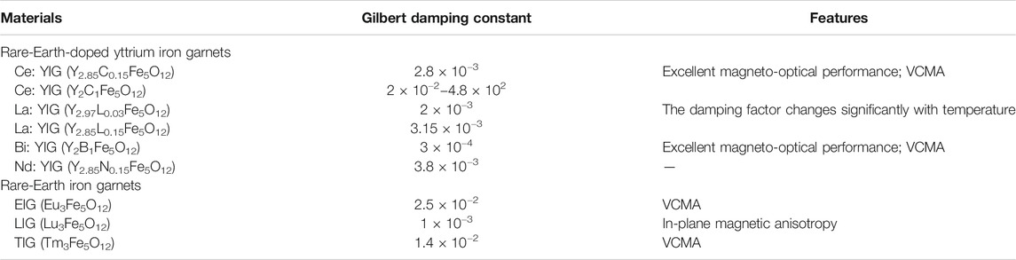
TABLE 3. Gilbert damping constant and other magnetic properties of YIG films modified by rare Earth elements.
Although modification of YIG with the rare Earth elements material does not improve Gilbert damping constant, it provides special advantages in magneto-optical and other magnetic properties. For instance, Bi: YIG and BIG provide the largest magneto-optical constant in the iron garnet family and its Faraday rotation angle reached 60°/μm in the visible light range (λ = 430 nm). Furthermore, Ce: YIG demonstrates both enhanced Faraday effect (Gomi et al., 1991) and enhanced magneto-optical Kerr effect (Kehlberger et al., 2015). These excellent magneto-optical properties are of great significance to the design of integrated magneto-optical devices such as isolators and circulators. In addition, YIG films modified by rare Earth elements Ce (Lage et al., 2017), Bi (Sellappan et al., 2017; Soumah et al., 2018), Eu (Rosenberg et al., 2018) and Tm (Quindeau et al., 2017) can be used to control the magnetic anisotropy of the films. By reducing the thickness of these modified YIG films to a certain extent, the films show perpendicular magnetic anisotropy. Some believe that this is due to the magnetoelastic anisotropy caused by the epitaxial mismatch strain of the film on the substrate (Sellappan et al., 2017; Rosenberg et al., 2018). Another explanation for this is that the transformation of the easy magnetic axis orientation is the result of competition between decreasing saturation magnetization and the constant uniaxial perpendicular anisotropy (Popova et al., 2013).
Topological Magnonics
The topological phase of matter and non-traditional chiral edge mode are believed to exist in various classical systems. The edge mode is robust to disturbances and is not sensitive to material parameters. Recently, the topological origin of the unidirectional magnetostatic surface spin waves has been deduced (Shindou et al., 2013; Yamamoto et al., 2019), implying that the topological phase of matter exists in a broader field including spintronics. For the first time, Chisnell et al. (2015) developed a two-dimensional topological magnon insulator, in which the degree of freedom of spin is similar to that of electrons in electronic topological insulators. This corroborates the existence of protecting chiral edge modes of spin waves. Collective spin excitations of chiral surface states were found in a three-dimensional topological insulator Bi2Se3 (Kung et al., 2017). Compared with the calculations, it is determined that this is a new type of transverse chiral spin waves, and the strong spin-orbit coupling ensures the robustness of the spin waves.
The polarized Raman spectrum of Bi2Sn3 was measured experimentally, showing a resonance peak at 150 meV. It was found that the experimental result is in coincidence with the theoretical result of transverse chiral spin waves (calculated Raman spectrum), determined that the mode of spin waves propagate in three-dimensional topological insulator Bi2Sn3 is transverse chirality. The main computational process of Raman response is as follows (for a more detailed calculation process, see reference Kung et al. (2017)):
The chiral surface state of three-dimensional topological insulators can be expressed by the Hamiltonian operator
where
The two terms in the right-hand side of Eq. 215, respectively, represent the interaction mechanism between holes to electrons, and holes to holes. Due to the characteristics of Bi2Se3, the second term is basically dispersion-free and the first term is small, which is consistent with the experiment (only one resonance is observed). The initial and final states of the Raman vertex form a 2 × 2 space, then the Raman response function is written as
Where
where
With the continuous in-depth research, spin waves with robust topological properties brought to the attention of the research community, see, e.g., Roldán-Molina et al. (2016) and Chen et al. (2018). Topological chiral edge spin waves (TESWs) generally exist in perpendicularly magnetized ferromagnets with a honeycomb lattice as shown in Figure 1A (Wang et al., 2018c). For example, Lu2V2O7 (Onose et al., 2010) with pyrochlore structure and Cu[1,3-bdc] (Chisnell et al., 2015) with kagome structure are topological magnetic materials. TESWs are a result of competition among Heisenberg exchange, Dzyaloshinskii–Moriya interaction and other physical mechanisms (Roldán-Molina et al., 2016; Chen et al., 2018), which are caused by spin-orbit coupling.
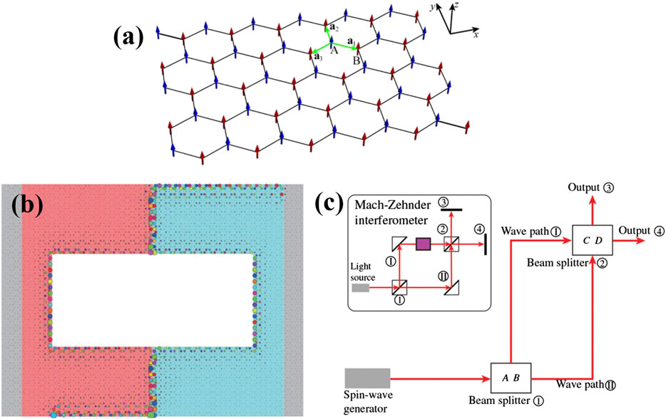
FIGURE 1. (A) Schematic diagram of perpendicularly magnetized ferromagnet with a honeycomb lattice for propagating TESWs. The blue and red arrows indicate the magnetic moment vectors on sublattices A and B. Green arrows are three adjacent site vectors a1, a2 and a3 (Wang et al., 2017). Reproduced with the permission from https://journals.aps.org/prb/abstract/10.1103/PhysRevB.95.014435. (B) TESWs interferometer, in which spin waves propagate or split along the domain walls, where the length of propagation path determines the phase and amplitude of spin waves (the size of different color symbols). In this setting interference occurs, where two spin waves with different phases are merged (Wang et al., 2018c). Reproduced with the permission from https://journals.aps.org/prapplied/abstract/10.1103/PhysRevApplied.9.024029. (C) Schematic diagram of TESWs interferometer in (B), the illustration is optical Mach-Zehnder interferometer and a beam enters beam splitter ① and gets divided into two beams, and the two beams are recombined at the second beam splitter ②, and the outputs ③ and ④ depend on the interference result of the two beams at beam splitter ② (Wang et al., 2018c). Reproduced with the permission from https://journals.aps.org/prapplied/abstract/10.1103/PhysRevApplied.9.024029.
This topological chiral edge mode is different from the traditional magnetostatic spin-wave mode but is similar to the topological protected edge state in electronic topological insulators. As shown in Figure 1B, the excited spin waves propagate in a single direction along the surface or edge of the sample and are insensitive to sample’s geometry, defects, and external disturbances. This enables utilization of such materials as an appropriate information carrier in spin-wave information applications (Wang et al., 2017). Due to the unique advantages of TESWs, Wang et al. (2017) and Wang et al. (2018c) proposed the concept of “topological magnonics” using sample edges and domain walls to control the propagation of TESW. This enables designing topological spin-wave diodes, beam splitters, and interferometers (Figure 1C), thus opens up a new research direction namely robust, reconfigurable and scalable topological spin-wave circuits.
Magnonic Crystals
Magnonic crystals are formed by periodically adjusting material parameters, see, e.g., Ciubotaru et al., (2013), Obry et al. (2013), Banerjee et al. (2017), and Richardson et al. (2018) or external fields, see, e.g., Chumak et al. (2009) and Ustinov et al. (2019). As an artificial magnetic crystal, magnonic crystals are an important component of spin-wave devices. By using the periodic characteristics of magnonic crystals, the dispersion relationship and propagation characteristics of spin waves can be adjusted statically or dynamically. This also enables spin-wave filtering and other functions. Figure 2A shows a magnonic crystal with a groove array, where the width and height of the groove determine the propagating characteristics of the passing spin waves (Richardson et al., 2018).
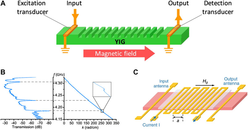
FIGURE 2. (A) A static magnonic crystal with a groove array, where the width and height of the groove determine the propagation characteristics of the passing spin waves (Richardson et al., 2018). Reproduced with the permission from https://journals.aps.org/prl/abstract/10.1103/PhysRevLett.121.107204. (B) The spin-wave propagation characteristics (left side) and the dispersion relationship (right side) of magnonic crystal in (A). It is clearly seen that spin waves are forbidden to a certain extent at specific frequencies (4.18, 4.23 and 4.3 GHz) known as “band gaps” while they can propagate freely in other frequencies (Richardson et al., 2018). Reproduced with the permission from https://journals.aps.org/prl/abstract/10.1103/PhysRevLett.121.107204. (C) A schematic diagram of dynamic magnonic crystal based on current regulation; by changing the current, the transverse magnetic field of the magnetic crystal is also changed, thus the propagation characteristics of the passing spin waves can be adjusted (Rana and Otani, 2019) (licensed under CC BY 4.0).
Figure 2B shows the spin-wave propagation characteristics (left side) and dispersion relationship (right side) of magnonic crystal in Figure 2A. It can be clearly seen that the spin waves are forbidden to a certain extent at specific frequencies (4.18, 4.23 and 4.3 GHz) known as “band gaps,” while other frequencies can freely propagate. This is because of period change in the width, thickness, internal and external field parameters of magnonic crystals. In this periodic structure, Bragg scattering has a certain impact on the spectrum of the spin waves and generate “band gaps” that exclude the transmission of spin waves (Chumak et al., 2017).
Table 4 presents the status of development in different magnonic crystals at home and abroad in detail, including classification, designing mechanisms, respective characteristics, and the corresponding realized applications. As shown in Table 4, magnonic crystals can be divided into three categories: static, reconfigurable, and dynamic. Among them, the geometry and inherent magnetism of the static magnonic crystals vary periodically, hence it is unchangeable once the magnonic crystal is manufactured (Choudhury et al., 2017; Sadovnikov et al., 2018). The magnetic properties of reconfigurable magnonic crystals can be changed as needed which means that the propagation characteristics of spin waves can be flexibly changed (Vogel et al., 2015; Albisetti et al., 2016). The magnetic properties of dynamic magnonic crystals can also be changed, and the adjustment speed is even faster than the spin-wave propagation speed. Figure 2C is a schematic diagram of dynamic magnonic crystal based on current regulation. By changing the current, the transverse magnetic field of the magnetic crystal is also changed, thus the propagation characteristics of the passing spin waves can be adjusted accordingly, see, e.g., Chumak et al. (2009) and Rana and Otani (2019).
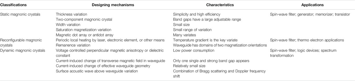
TABLE 4. Classifications, designing mechanisms, respective characteristics and realized applications of magnonic crystals.
As a typical representative of the structure design of spin-wave materials, magnonic crystals are widely used in spin-wave devices. Filtering characteristics of magnonic crystals also facilitate building spin-wave filters. In addition to the filtering function, magnonic crystals are used in spin-wave logic devices (Nikitin et al., 2015), spin-wave transistors (Chumak et al., 2014), and spin-wave thermo electron applications (Albisetti et al., 2016), etc., and play a significant role in versatile development of multifunctional spin-wave devices.
Interfacial Magnetoelectric Effects
Voltage-Controlled Magnetic Anisotropy
Magnetic properties of materials controlled by electric field (voltage) are seen in many material systems. For example, in ferromagnetic materials, the magnetism can be manipulated by changing the number and density of charge carriers, while in multiferroic materials, coupling between electric field and magnetization occurs through electrical polarization (Matsukura et al., 2015). Voltage-controlled magnetic anisotropy (VCMA) generally occurs in metal (ferromagnet)/metal oxide (insulator) structures and can be also referred to as electrical manipulation of interfacial perpendicular magnetic anisotropy (iPMA). The most common VCMA structure is Fe (Co)/MgO heterojunction. Applying an electric field in the interface between the metal film and insulator, due to the spin-orbit coupling interaction (Fe 3d-orbitals of strongly bond with the O 2p-orbitals) leading to charge transfer from 3d-orbitals to 2p-orbitals. Because the occupancy of 3d-orbitals electrons determines the direction and magnitude of magnetic anisotropy of ferromagnet films, the applied electric field can be used to control iPMA (Rana and Otani, 2019). The Fermi energy position at the interface is also changed due to hybridization between the orbits. This can be considered as an adjustment of Fermi energy position on magnetic anisotropy (Matsukura et al., 2015). Furthermore, in VCMA the change of iPMA is linearly proportional to the applied electric field (Duan et al., 2008), i.e., ΔKS = βE, where ΔKS is the change of iPMA and β is VCMA coefficient.
VCMA provides a breakthrough for the development of spin-wave devices and spin-wave manipulations. The conventional methods of controlling spin waves by current-induced Oersted field or spin-transfer torque increase the thermal management cost and further damages the life cycle of the devices. The spin-wave manipulation methods based on VCMA however only need enough electrons to charge and discharge the capacitor. This significantly reduces the power dissipation and adds non-volatile function compared to the charge-current methods (Matsukura et al., 2015). In the following we introduce the basic operations of VCMA including spin-wave excitation, conduction, phase shift and amplification.
Spin-wave excitations by VCMA can be divided into linear and nonlinear parametric excitations. Conventional parametric excitation system requires a high threshold value of the magnetic field which leads to a high energy consumption and Joule heating (Urazhdin et al., 2010). In this context, VCMA achieves nonlinear parametric excitation with a lower energy consumption in an elliptical nano magnetic tunnel junction (see Figure 3A; Chen et al., 2017). The magnetization direction of Co20Fe60B20/MgO interface is also controlled by the voltage instead of the magnetic field pumping used in the original system. Spin waves are excited by nonlinear parameters where VCMA is combined with magnetization parameter resonance. The driving voltage is as low as 0.136 V which reduces the threshold value and energy consumption of the process. However, the nonlinear relationship and the amplitude of excited spin waves results in complexities in the application of spin-wave logic devices, and a certain value of threshold is still needed. To solve this issue, a linear parametric excitation method based on VCMA is proposed in Rana et al. (2017). As shown in Figure 3B, the top strip Au electrode is deposited on the waveguide made of multi-layer thin film. Further, the perpendicular magnetic anisotropy at the interface between CoFeB and MgO is regulated by applying a radio frequency (RF) voltage on the electrode. Spin waves with short wavelength are locally excited in linear form without requiring a voltage threshold as shown in Rana et al. (2017).
FIGURE 3. Spin-wave excitation devices based on VCMA. (A) Schematic diagram of nonlinear parameter excitation device. Due to iPMA, Co20Fe60B20 magnetization equilibrium direction is perpendicular to the plane. In cases where the microwave voltage frequency applied by the top electrode is twice of the spin-wave frequency, short wavelength spin waves are excited (Chen et al., 2017). Reprinted with the permission from Chen, Y.-J., Lee, H.K., Verba, R., Katine, J.A., Barsukov, I., Tiberkevich, V., et al. (2017). Parametric resonance of magnetization excited by electric field. Nano letters 17 (1), 572-577. Copyright 2017 American Chemical Society. (B) Schematic diagram of linear parameter excitation device: applying an RF voltage on Au electrode to locally excite spin waves (Rana et al., 2017) (licensed under CC BY 4.0).
One of the difficulties in using spin waves to replace charge-currents as information transport carrier is to find solution to control spin waves propagation as effectively as using voltage to control the current flow. There are several techniques to design the spin-wave propagation channel among them making the spin-wave waveguide into strips has been investigated in Urazhdin et al. (2014) and Vogt et al. (2014). The issue however is that once the waveguide is completed, the function is fixed. Another technique is to control the propagation of spin waves by using Oersted field inside the waveguide (Sadovnikov et al., 2016; Heussner et al., 2017). In this technique, Oersted magnetic field is driven by direct current. As mentioned before, this inevitably brings about a high energy consumption as well as nonlocal Oersted field problems. VCMA also provides a new approach for designing spin-wave nano propagation channels. Using micromagnetic simulation, Rana and Otani (2018) showed that the spin-wave propagation channels designed based on VCMA are very simple. They further showed that these channels provide a unique advantage by controlling a few closely spaced spin-wave nanochannels at the same time. As shown in Figure 4A, by applying a positive voltage to the electrode above the waveguide, a perpendicular magnetic anisotropy is created in the direction out of the plane. This induces the magnetostatic forward volume-like spin waves that are propagated along X direction in the electrode covering area of the waveguide. The propagation of spin waves is terminated by setting the electrode voltage to 0 (see Figures 4B–D). Based on this principle, a variety of spin-wave nanochannels are designed including single channel, multi-channels, curved channel and Y-shaped channel. It is also shown in Rana and Otani (2018) that by using VCMA, the spin waves can be effectively switched in multiple channels.
FIGURE 4. (A) Top view of the waveguide (Rana and Otani, 2018). Due to VCMA, three spin-wave channels with a width of 100 nm are formed by three separate metal electrodes. (B–F) Spatial distribution diagram of dynamic magnetization. (B) A voltage is applied to the upper electrode to form a spin wave-channel; (C) A voltage is applied to the middle electrode to form a spin-wave channel; (D) A voltage is applied to the lower electrode to form a spin-wave channel; (E) Three spin-wave channels can be opened simultaneously; (F) Different phase accumulation occurs, where spin waves with different wave vectors pass through the waveguide. (A–F) Reproduced with the permission from https://journals.aps.org/prapplied/abstract/10.1103/PhysRevApplied.9.014033.
Spin-wave phase shifter is one of the key components in spin-wave logic devices (Kostylev et al., 2005; Lee and Kim, 2008). The phase shift operation of spin waves is usually completed using Oersted magnetic field induced by current (Schneider et al., 2008; Hansen et al., 2009). In addition to producing a lot of Joule heat, this also affects the normal operation of other components because of the nonlocality of Oersted field. Rana and Otani (2018) realized XNOR and NAND gates by the phase shifters based on VCMA. The underlying mechanism is that VCMA affects the spin-wave dispersion, therefore, applying a positive voltage to the electrode, increases the vector of the spin waves passing through the waveguide. As shown in Figure 4F, different voltage values are corresponded to different wave vectors. Note that the spin-wave phase is equal to the product of wave vector and the propagation distance. Therefore, different phase accumulation occurs, where spin waves with different wave vectors pass through the waveguide under the action of VCMA.
In addition to the above basic operations, VCMA may be used for spin-wave amplifications. There is no study on directly inducing the amplitude enhancement of spin waves by VCMA, but some researches have shown that indirect amplification of spin waves can be achieved by reducing the magnetic damping of materials (Divinskiy et al., 2018). Okada et al. (2014) found that where the film thickness is determined, Gilbert damping constant and interface magnetic anisotropy energy density are linearly decreased with increasing the applied electric field while the modulation ratio is fixed. In a case where the film thickness is 1.4 nm, by increasing the voltage from 0 to 0.15 V the damping constant decreases from 0.0126 to 0.0122. Although the attenuation degree is only 3%, it is expected to effectively reduce the spin-wave damping by increasing the electric field intensity and modulation ratio. Although both the damping constant and the VCMA are explained by the second-order perturbation of the spin-orbit interaction (Bruno, 1989; Kamberský, 2007), the research on the relationship between them is still nonexistence.
Magneto-Inonic Transport
Previous studies have shown that ion migration in materials changes the thermal conductivity (Padture et al., 2002), optical properties (Lu et al., 2017), electrical conductivity (Waser et al., 2009), magnetic properties (Bi et al., 2014), etc. Various functions in new devices can be achieved by using the electric field-controlled ion migration effect. The modulation of magnetic moments and anisotropy through ion migration is called magneto-ionic transport. This can influence the hybridization of 3d-orbitals in ferromagnets and 2p-orbitals in oxygen on oxides, thereby modulating the VCMA effect between interfaces (Li et al., 2017). Magneto-ionic transport can also effectively improve the magnetism controlling efficiency, reduce the processing power consumption, and increase the operation speed which are beneficial in development of spintronic devices.
Magneto-ionic transport can be divided into two categories according to the different transporting ions. The first category is anion transportation represented by oxygen ion (Bi et al., 2014; Bauer et al., 2015; Gilbert et al., 2016a; Gilbert et al., 2016b; Grutter et al., 2016; Li et al., 2017), and the second is cation transportation including lithium and hydrogen ions (Dasgupta et al., 2016; Zhu et al., 2016; Tan et al., 2019). Oxygen ion transportation usually occurs in metal/metal oxide heterostructures. The principle of material selection should not only consider the VCMA effect between interfaces, but also ensure a sufficiently low activation energy for ion transportation. Figure 5A shows a typical magnetic heterostructure: Co/GdOx, in which GdOx material has high oxygen ion mobility which provides guarantee for effective transportation of ions in heterostructure controlled by the electric field (Bi et al., 2014; Bauer et al., 2015). Transportation of lithium ions also requires involvement of metal oxides with a lower activation energy, such as LiFe5O8 (Zhu et al., 2016), and Li0.72CuFe2O4 (Dasgupta et al., 2016). Controlling the magnetic properties of materials by lithium ion transportation usually requires participation of other metal ions. For example, the redox reaction of Fe ions (Zhu et al., 2016) or Cu ions (Dasgupta et al., 2016) occurs in the process of lithium ion delamination or intercalation. The magnetic properties of materials are changed by the chemical properties of Fe or Cu ions.
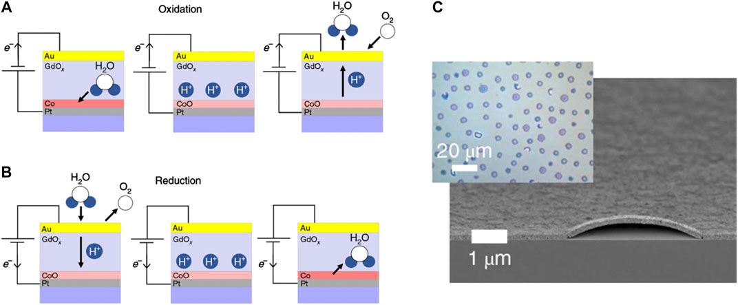
FIGURE 5. (A,B) Schematic diagram of Co/GdOx heterostructure and ongoing electrochemical reactions (Tan et al., 2019). (A) Applying a negative bias voltage causes an oxidation reaction at the anode: Co will be transformed into non-magnetic CoO material, and the magnetism will be eliminated; (B) Applying a positive bias voltage causes a reduction reaction at the cathode: CoO is converted into metal Co, recovering perpendicular magnetic anisotropy across the Co/GdOx interface; (C) Cross-sectional scanning electron microscope image of hydrogen accumulation after the positive bias voltage is continuously applied. (A–C) Reprinted with permission from Tan, A.J., Huang, M., Avci, C.O., Büttner, F., Mann, M., Hu, W., et al. (2019). Magneto-ionic control of magnetism using a solid-state proton pump. Nature materials 18 (1), 35–41. Copyright 2019 Springer.
Due to the oxidation or reduction reactions that occur during ion migration, the magneto-ionic transport can also be considered as electrochemical control of magnetism. Taking Co/GdOx heterostructure in Figures 5A,B as an example, by applying a negative voltage bias (Figure 5A), an oxidation reaction occurs at the anode. Co is then transformed into non-magnetic CoO material and the magnetism is completely eliminated. By applying a positive voltage bias (Figure 5B), a reduction reaction is occurred at the cathode and CoO is converted into metal Co, recovering perpendicular magnetic anisotropy across the Co/GdOx interface. Nevertheless, by continuous application of a positive bias, the out-of-plane perpendicular magnetic anisotropy at the interface cannot be preserved forever and turns into in-plane magnetism. There are two explanations for this observation. Bi et al. (2014) believed that when the reaction proceeded to an appropriate level and Co was embedded in CoO to form superparamagnetic Co islands, the perpendicular magnetic anisotropy could be formed at the interface, otherwise, when CoO layer is completely reduced to continuous Co layer in the metal state, only in-plane magnetic anisotropy is presented. Tan et al. (2019) believed that this phenomenon was caused by the accumulation of hydrogen atoms at the interface. They further experimentally observed bubbles formed by hydrogen accumulation (Figure 5C). When the circuit is disconnected, the redox reaction is interrupted due to the inability of electrons to move. Therefore, hydrogen atoms remain at the interface and cannot be removed, thus in-plane magnetism remains in the Co layer. By closing the circuit, the hydrogen atoms are then expelled from the device in the redox reaction, therefore the in-plane magnetism is disappeared and replaced by the perpendicular magnetic anisotropy.
With the assistance of magneto-ionic transport, the process of controlling magnetism by electric field becomes quicker and more convenient, enabling further development of voltage-controlled spintronic devices. Electronically controlled ion migration however still needs further improvements in the following aspects. Firstly, the switching speed at room temperature needs to be increased. The switching time of modern hard disk drives is as small as 10 ms while it usually takes several minutes for oxygen ions to migrate at high temperature (>100°C) and produce a large enough magnetic transition (Bi et al., 2014; Bauer et al., 2015). Although the existing Co/SrCoO2.5 heterostructures are capable of achieving a switching time of 0.2 ms at room temperature, its coercive force is only a few Oersted which limits its practical applications (Li et al., 2017). Secondly, reliability and non-volatility of these devices need to be enhanced. Although hydrogen ion migration has achieved more than 2,000 cycles at a relatively high speed (Tan et al., 2019), the device retention time can only last for a few days, which is not conducive to permanent data storage. PdH, a hydrogen storage material used in hydrogen ion transportation, has a high hydrogen mobility, but it is easy to eject hydrogen under vacuum or high temperature conditions (Gilbert et al., 2017). Therefore, finding a hydrogen storage material with higher quality is one of the next important challenges to be addressed.
Electrical Spin-Torque and Magnon-Torque
Electrical spin-torque can be divided into spin-transfer, and spin-orbit torque depending on its generation mechanisms. It is usually used to flip the magnetic moments of magnetic domains and is considered as the process of transferring spin angular momentum. Magnon-torque which is derived from magnon currents (spin waves), and electric spin-torque have similar functions but they are different in other aspects. These two kinds of torques existing in different heterostructures are widely used in switching magnetization of material and other fields. In the following we introduce them separately.
Existence of the spin-transfer torque (STT) effect was predicted by Berger (1996), and Slonczewski (1996), in 1996. Many experimental studies also confirmed its existence in the multilayer structures (such as Co/Cu/Co) composed of ferromagnetic and non-ferromagnetic films alternately (Tsoi et al., 1998; Myers et al., 1999; Katine et al., 2000). STT is usually observed with giant magnetoresistance effect as probe (Katine et al., 2000). By passing current through a magnetic tunnel junction vertically, the spin angular momentums carried by conducted electrons are transferred to the localized electrons in the free layer. This changes the relative magnetization direction between free layer and fixed layer as well as the resistance of magnetic tunnel junction (Myers et al., 1999). There are usually two mechanisms for the STT to change the magnetic properties of the thin films both based on polarized electrons to reverse the magnetization direction of the free layer. The electrons in the first mechanism are polarized under the positive influence of the reference layer. The polarization direction is parallel to the reference layer, therefore, passing the polarized electrons through a thin free layer forces the magnetization direction of the free layer to become parallel with the direction of the reference layer. In the second mechanism the polarized electrons are formed due to the negative influence of the reference layer. The polarization direction is the opposite to that of the reference layer, therefore, flowing the electrons through the free layer forces the magnetization direction of the free layer becomes antiparallel to that of the reference layer.
Spin-orbit torque (SOT) usually exists in a two-layer structure composed of ferromagnet and nonmagnetic heavy metal (platinum, tantalum, tungsten, etc.) films (Fukami et al., 2016). In SOT, similar to the STT, the spin-torque of the polarized current is used to flip the magnetic moments of the magnetic domains (Katine et al., 2000). Once direct current flows through the plane of nonmagnetic heavy metal film at a certain angle, spin current is induced in a direction perpendicular to the thin films thus spin-torque is exerted on the magnetic moment of ferromagnet and changes its magnetization direction. In SOT, the spin-torque may be caused by Rashba effect (Emori et al., 2016), or Spin Hall effect (Fukami et al., 2016), or both (Fan et al., 2014), but it can be eventually interpreted as a strong spin-orbit coupling between heavy metal materials, therefore, the spin-torque is called the spin-orbit torque.
Magnetoresistive random access memory (MRAM) can be directly constructed under electric control based on STT and SOT, instead of using magnetic field generated by current to reverse magnetization in traditional magnetoresistive effect. This provides a significant practical value (Fong et al., 2016; Nozaki et al., 2019). STT-MRAM can achieve the level of integration density similar to the DRAM (Dynamic RAM), while obtain an excellent performance level similar to the SRAM (Static RAM). Although STT-MRAM is compatible with the CMOS manufacturing process, there exist some performance issues related to the energy efficiency of writing (Fong et al., 2016). As an improved version of STT-MRAM, SOT-MRAM provides more advantages. Since spin-orbital torque in SOT-MRAM is originated from heavy metals, the writing path does not pass through the magnetic tunnel junction and is separated from the reading path. Therefore, barrier breakdown can be almost avoided. The spin-orbit torque also achieves a higher writing speed due to the perpendicular magnetic anisotropic magnetic tunnel junction (Nozaki et al., 2019). Currently, almost all types of memories are faced with the dilemma of stable non-volatility and high working energy. It is believed that STT/SOT-MRAM will be able to make an important impact on the development of new memories with a low working and standby energy consumption.
In addition to their applications in memory, STT and SOT play an important role in spin-wave manipulation and the development of spin-wave devices (Madami et al., 2011; Divinskiy et al., 2018; Houshang et al., 2018; Fulara et al., 2019). Madami et al. (2011) used STT effect to excite spin waves in a multilayer heterostructure as shown in Figure 6A (CoFe layer as reference/fixed layer and NiFe layer as free layer). They managed to show the existence of propagating spin waves as opposed to localized spin waves. It is also found that a negative excitation current results in detecting a higher intensity of spin-wave intensity much larger than that of thermal spin-wave intensity. Interestingly, by applying a positive current the spin-wave signal cannot not be detected. It is concluded that the spin-wave frequency is linearly proportional to the injected direct current. Divinskiy et al. (2018) found that SOT is capable of achieving the excitation of coherent propagating spin waves. They also show that SOT is also capable of spin waves amplification by compensating Gilbert damping in the spin-wave propagation. The experimental diagram is shown in Figure 6B. By combining theory with experiment, it was also proved that the anti-damping torque brought by spin current can, to a certain extent, compensate the propagation damping of spin waves. According to damping compensation formula:
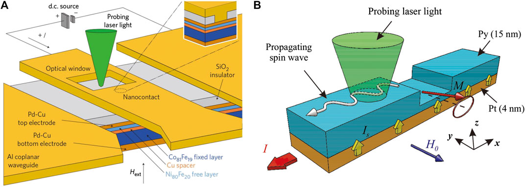
FIGURE 6. (A) Cross-section of spin-wave excitation device based on STT. An aluminum coplanar waveguide is deposited on the STT multilayer structure, and an optical window is etched on the waveguide conductor center near the nanocontact point. Polarized current is injected into the STT structure through the nanocontact point to realize spin-wave excitation (Madami et al., 2011). Reprinted with permission from Madami, M., Bonetti, S., Consolo, G., Tacchi, S., Carlotti, G., Gubbiotti, G., et al. (2011). Direct observation of a propagating spin wave induced by spin-transfer torque. Nature nanotechnology 6 (10), 635. Copyright 2011 Springer. (B) Schematic diagram of spin-wave excitation and amplification device based on SOT. A current in the direction of -x is applied to the permalloy (Py) layer, and a spin polarized current in the direction of z is generated. The Py layer is the spin-wave waveguide with a rectangular notch with a width of 200 nm and a depth of 10 nm in the center. By complete compensation of the damping at the waveguide notch, the spin wave is generated at the notch and propagated along the -x direction. The spin wave is then amplified during propagation (Divinskiy et al., 2018). Reproduced with the permission from https://doi.org/10.1002/adma.201802837.
Magnon-torque is different from electric spin-torque in that the former comes from spin waves and the latter from spin currents. In contrast to the spin currents, no electron flow is required in spin-wave propagation. Therefore, the effects of joule heat are avoided as well as the corresponding power consumption. Furthermore, as it is seen in Table 1 the mean free path of spin-wave propagation is usually a few microns that even exceeds the propagation distance of 1,000 microns in high-quality bulk YIG. Nevertheless, the dissipation distance of spin currents is only on the nanometer scale (Bass and Pratt Jr, 2007). Because of the above advantages, it is of great scientific value to use magnon-torque to reverse the magnetization direction of materials. Wang et al. (2019) reported promising experimental results for magnetization switching based on magnon-torque.
Figure 7A shows the schematic diagram of a spin-torque ferromagnetic resonance (ST-FMR) measurement system. It is seen that the magnon current (spin waves), JM, induced by RF current, JC, is propagated perpendicular to the film plane, passes through NiO layer, and reversing the magnetization direction of NiFe layer. NiO is the only carrier of magnon current because it can isolate the spin polarized current. Figure 7B shows the variation of spin-torque ratio, θi, for three NiO layers with different thicknesses versus temperature, T, in which θi = Ji/JC represents the generation ratio of input current to magnon current. At thickness of tNiO = 25 nm, the spin-torque ratio is generally high, with the maximum value exceeding 0.4, and 0.3 at the room temperature, which is close to the electric spin-torque ratio (about 0.67). Experiments further confirmed that this magnon-torque is mainly affected by the magnon current rather than other factors (temperature, Oersted magnetic field, etc.). Experiments also corroborate successful realization of magnetization switching of permalloy (Py) in Bi2Se3/NiO/Py and Bi2Se3/NiO/Cu/Py heterostructures.
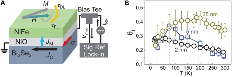
FIGURE 7. (A) Schematic diagram of spin-torque ferromagnetic resonance (ST-FMR) measurement system (Wang et al., 2019). JC is the RF current, σ is spin polarization direction, and JM is magnon current. (B) Variation of spin-torque ratio θi of three NiO layers with different thicknesses versus temperature T, where θi = Ji/JC represents the generation ratio of input current to magnon current. (A–B) Reprinted with permission from Wang, Y., Zhu, D., Yang, Y., Lee, K., Mishra, R., Go, G., et al. (2019). Magnetization switching by magnon-mediated spin torque through an antiferromagnetic insulator. Science 366 (6469), 1125–1128. Copyright 2019 American Association for the Advancement of Science.
Application of magnon-torque in magnetization switching caused a paradigm change in the related fields of studies especially in magnon transport, and further broadened the scope of research on spintronics. In the current state-of-the-art, however, the generation of magnon-torque still needs external current injection and the efficiency of magnetization switching is lower than that of mature electric spin-torque (STT and SOT). With the continuous innovation of research on excitation and transportation of magnons (spin waves), we expect to see the application of magnon-torque in magnetic applications such as MRAM.
Functional Spin-Wave Devices
Information Processing Devices
Spin-wave devices take spin-wave as the carrier of information transmission and processing. Compared with the traditional CMOS devices which take charge-current as the carrier, low power consumption is one of the biggest advantages of spin-wave devices. However, many operations (such as excitation, phase shifting and amplification) of spin waves require external energy or other forms of assistance. To meet the requirements in ultra-low power consumption of spin-wave devices, it is not sufficient to only focus on the energy dissipation in the process of spin-wave propagation. It is further essential to reduce the power dissipation during the manipulation of spin waves. This is one of the main motivations behind continuous development of the spin-wave information processing devices. With the involvement of electrical current or voltage (Sekiguchi et al., 2012), and various novel interface effects (Rana and Otani, 2018; Wang et al., 2018b), researchers have designed a variety of spin-wave electronic devices, such as spin-wave phase shifter, signal splitter, and logic gate. Phase shifter is one of the most critical components in the spin-wave logic circuits. By adjusting the phases of two or more beams of spin waves from the same source, interference occurs upon their convergence resulting in the signal of spin-wave to be weakened, or strengthened corresponding logical value of 0 or 1, respectively.
Charge-current based electrical method is one of the main techniques used in the earlier spin-wave electronic devices (Lee and Kim, 2008). In 2008, Schneider et al. (2008) used Oersted field generated by current to regulate and design a phase shifter, as shown in Figure 8A. Oersted field affects the transmission dispersion of spin-wave and causes phase shift in spin-wave. By cutting of the current, Oersted field disappears and the spin-wave original propagation characteristics are recovered. However, in this method, using electric current causes a high-power consumption and the corresponding Joule heat may become unacceptable. Furthermore, the application area of Oersted field is difficult to be accurately controlled. This may affect other components in the system. In order to reduce the influence of Joule heating, in 2015, Zhong et al. (Wang et al., 2014; Chen et al., 2015; Chen et al., 2016) proposed using the polarized spin current generated by the STT effect to directly act on the waveguide. This changed the magnetization state of the original spin-wave, resulting in phase shifting as shown in Figure 8B. The experimental results show that a 180° phase shifting effect can be achieved using three phase shifters.
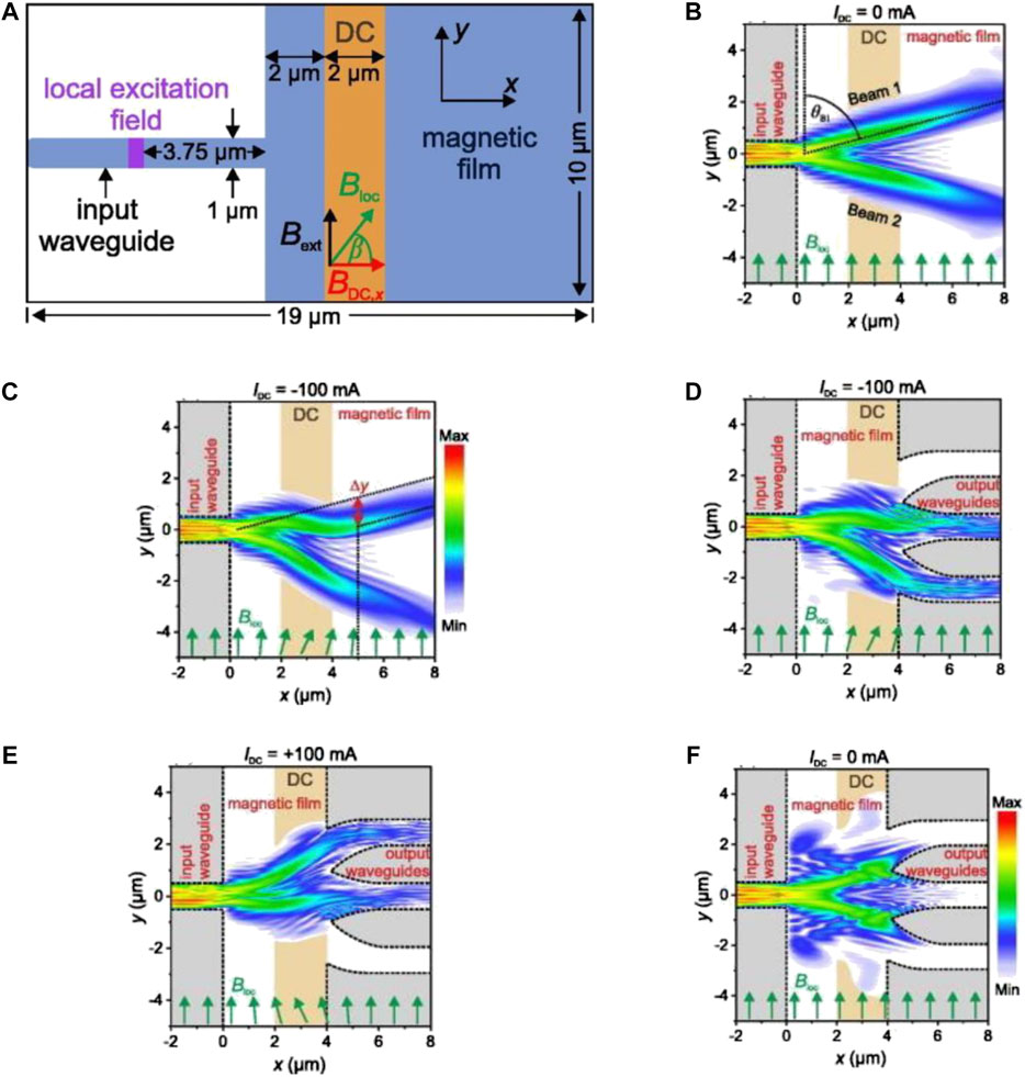
FIGURE 8. Spin-wave signal divider based on charge current. (A) Schematic diagram of simulation structure (Heussner et al., 2017). (B–F) Dynamic magnetization results. (B) Without applied current; (C) Applying a negative direct current of −100 mA; (D) Switching between waveguides after applying a negative direct current of −100 mA; (E) Switching between waveguides after applying a positive direct current of 100 mA; (F) Switching between waveguides without applied current. (A–F) Reprinted from Heussner, F., Serga, A., Brächer, T., Hillebrands, B., and Pirro, P. (2017). A switchable spin-wave signal splitter for magnonic networks. Applied Physics Letters 111 (12), 122401. With the permission of AIP Publishing.
The signal splitter is of great significance for selective switching of spin-wave signals where there are multiple spin-wave channels. In 2017, Heussner et al. (2017) designed a spin-wave signal splitter based on charge-current. As shown in Figure 8A, a direct current is applied along the y-axis in the brown region to generate an Oersted field, while an external y-axis bias magnetic field is applied across the whole device. The spin wave is excited from the left end and then propagates to the right end. Compared with the original case, in which the spin waves can only propagate at a specific angle (Figure 8B), it is found that the spin-wave transmission trajectory can be adjusted under the action of Oersted field after applying a 100 mA current (Figure 8C). This is because Oersted field generated by current causes deviation in the direction of total magnetic field from the original external magnetic field in a certain angle, thus changing the dispersion of spin-wave and further changing the trajectory of transmission. Based on this principle, a signal splitter for connecting different waveguides is designed, as shown in Figures 8D–F. Since it can realize switching and on-off control between different waveguides, it is very beneficial to the circuit design of multistage cascade. Furthermore, the spin-wave multiplexer was realized by charge-current (Vogt et al., 2014) and the spin-wave directional coupler was realized by spin-wave dipole exchange effect (Yu et al., 2013; Wang et al., 2018a).
There still exist many issues in charge-current based spin-wave electronic devices. Oersted field and other related effects induced by current input are difficult to be control accurately in the whole system. Furthermore, a large amount of Joule heat generated during operation have negative effects on micro/nano-scale spin-wave electronic devices. To address this issues research attention was directed to voltage-controlled spin-wave electronic devices. In 2011, Liu and Vignale (2011), the electric field is used to directly manipulate the spin-wave dispersion and realized the effective control of the spin-wave phase under the spin-orbit coupling. As it is seen in Figure 9A, the electric field radiates from the center to the annular waveguide. A series of micro coupling effects occur during the spin-wave passing through the waveguide which result in a phase shift of 180°. This can be used for the designing spin-wave interferometer which then lays a foundation for the development of ultra-low power consumption spin-wave logic devices. This is because the phase-shifting process of spin-wave does not require current input. Different from the spin-orbit coupling effect, other researchers proposed a designing method for the spin-wave phase shifter accomplished by electric field through electromagnetic coupling and Dzyaloshinskii-Moriya interaction (DMI) (Wang et al., 2018b). Figure 9B is a schematic diagram of this phase shifter. Under the action of the left electric field application area, the dispersion of spin-wave appearing asymmetric structure during propagation to the right. Therefore, different phase offsets appear under different electric field intensities. In Voltage-Controlled Magnetic Anisotropy, we also discuss spin-wave phase shifting operation based on VCMA.
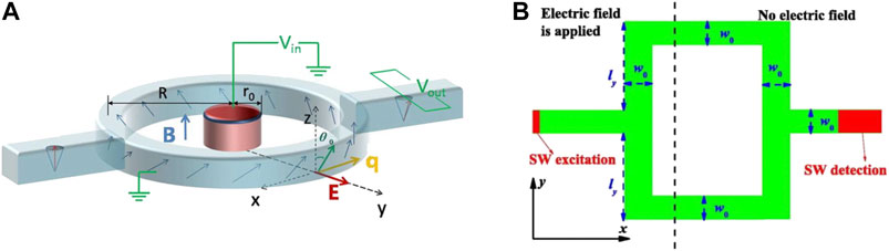
FIGURE 9. (A) Schematic diagram of voltage-controlled spin-wave phase shifter based on spin-orbit coupling interaction (Liu and Vignale, 2011). Reproduced with the permission from https://journals.aps.org/prl/abstract/10.1103/PhysRevLett.106.247203. (B) Schematic diagram of voltage-controlled spin-wave phase shifter based on DMI (Wang et al., 2018b). Reprinted from Wang, X.-g., Chotorlishvili, L., Guo, G.-h., and Berakdar, J. (2018). Electric field-controlled spin waveguide phase shifter in YIG. Journal of Applied Physics 124 (7), 073903. With the permission of AIP Publishing.
In addition to the electrical methods, using domain walls to control the phase and amplitude of spin waves is another important modulation method (Han et al., 2019). Figure 10A is the experimental setup, Figures 10B,C are the magneto-optical Kerr effect (MOKE) images of the devices, in which the bright and dark colors represent the domains with up and down magnetization. An obvious domain wall can be observed in the device of Figure 10C, while the device in Figure 10B is uniform. Figure 10D is the simulated propagation of spin waves, the upper and lower waveguides for spin-wave propagation corresponding to (b) uniform state and (c) domain wall state, respectively. The single dotted line indicates an inserted domain wall and the dotted rectangular indicates a phase shifting of nearly 180° after spin-wave passing through the domain wall. Han et al. proved that the phase shift induced by magnetic domain wall will not be influenced by magnetic domain configuration (i.e., up-down or down-up), and the deviation of five experimental phase shifting results is less than 10%. In addition, the amplitude of spin-wave is decreased by a factor of 4.3 times after passing through the domain wall. It is due to the reflection of spin-wave at the domain wall edge caused by the quasi-rigid boundary condition of the magnetic moments.
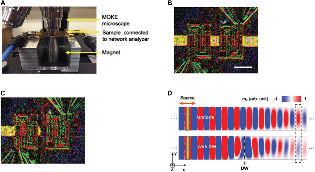
FIGURE 10. (A) Experimental setup for controlling the phase and amplitude of spin waves by a domain wall (Han et al., 2019). (B), (C) Magneto-optic Kerr effect (MOKE) images. The light and dark colors represent domains with opposite magnetization directions. In (B) the waveguide is uniform, and in (C) there is a domain wall in the middle of the waveguide. (D) Simulation diagram of spin-wave propagation. The upper and lower waveguides correspond to (B) uniform state and (C) domain wall state, respectively. The single dotted line indicates an inserted domain wall and the dotted rectangular indicates a phase shifting of nearly 180° after spin-wave passes through the domain wall. (A–D) Reprinted with permission from Han, J., Zhang, P., Hou, J.T., Siddiqui, S.A., and Liu, L. (2019). Mutual control of coherent spin waves and magnetic domain walls in a magnonic device. Science 366 (6469), 1121–1125. Copyright 2019 American Association for the Advancement of Science.
The author further studied the interaction between spin waves and magnetic domain wall, and finds that the position of magnetic domain wall is changed after spin-wave passing through it, and the magnetic domain wall always moves against the flow direction of spin-wave. This is attributed to the effect of spin-torque in magnon current. The mutual control between the spin waves and the domain wall means that all the operations in the spin-wave devices can be completed by only one spin-wave. This provided the possibility of the realization of all-magnon spin-wave devices.
As it is seen in the above, phase shifting operation based on charge-current is associated with high level of power consumption and the generated Oersted field reduces the operational accuracy of spin-wave devices. New spin-wave information processing devices are being developed with low power consumption, compatibility with micro/nano-scale devices and non-volatility. The ultimate goal is to realize all-voltage-controlled or all-magnon spin-wave logic devices in which voltage-controlled spin-wave device only needs enough electrons to charge and discharge a capacitor, and all-magnon spin-wave device can be achieved without any intervention of external field.
Spin-Wave Sensors
Sensors are often used to transform measured information into information that can be directly read, e.g., electrical signals. In recent years, with the continuous development of magnetism researches, the concept of spin-wave sensors is formed. In spin-wave sensors the output is not in form of electrical signal but spin-wave signals. In addition to energy conservation efficiency and avoiding the influence of Joule heating there are other reasons to pursue such sensors. In the following, we introduce several spin-wave sensors with different sensing functions including gas sensors (Matatagui et al., 2015b; Matatagui et al., 2017), magnetic sensors (Inoue et al., 2011; Goto et al., 2015), and humidity sensors (Matatagui et al., 2015a) and further discuss their basic operational principles and characteristics.
Aiming at gas identification and detection, researchers from The National Autonomous University of Mexico (Matatagui et al., 2015b; Matatagui et al., 2017), successively developed a toxic gas sensor in 2015 and improved its performance in 2017. This initiated a new field of research on “magnonic e-noses.” In this sensor, magnetic nanoparticles react with gas to induce a frequency shift to the spin-wave oscillator. This ensures high sensitivity, short response time, good reproducibility and recyclability. Figures 11A,B illustrate the basic structure, and working principle of the gas sensor, respectively. Once the magnetic nanoparticles layer reacts with the gas in the environment, the total magnetic field of the sensor system will be affected. This changes the oscillation frequency of the magnetostatic surface spin-wave oscillator. Since the frequency shifts caused by different gases are different, the sensor can identify all kinds of gases (Matatagui et al., 2015b). On this basis, Matatagui et al. (2017) added the types of nanoparticles and formed a gas sensor array composed of CuFe2O4, ZnFe2O4, MnFe2O4 and CoFe2O4 particles. Due to the different sensitivity of various nanoparticles to a given type of gas by combining four sensing results through certain calculations classification accuracy of 100% was achieved. This gas sensor is not only excellent in performance, but also simple and inexpensive. However, it needs further researches in practical applications such as identifying or detecting the components of a mixed gas and distinguishing between different gases with different levels of concentrations.
FIGURE 11. (A) Schematic diagram of the spin-wave gas sensor composed of multilayer films (Matatagui et al., 2015b). (B) Working principle diagram of the spin-wave gas sensor (Matatagui et al., 2015b). (A,B) Reprinted from Matatagui, D., Kolokoltsev, O., Qureshi, N., Mejía-Uriarte, E., and Saniger, J. (2015). A magnonic gas sensor based on magnetic nanoparticles. Nanoscale 7 (21), 9607–9613. With the permission of RSC Publishing. (C) Variation of band gap frequency of magnonic crystal in the spin-wave magnetic field sensor with increasing external bias magnetic field. The black arrows represent the change in the band gap frequency caused by increasing theapplied magnetic field. The change in band gap frequency affects the propagation characteristics of spin-wave (Inoue et al., 2011). Reprinted from Inoue, M., Baryshev, A., Takagi, H., Lim, P.B., Hatafuku, K., Noda, J., et al. (2011). Investigating the use of magnonic crystals as extremely sensitive magnetic field sensors at room temperature. Applied Physics Letters 98 (13), 132511. With the permission of AIP Publishing. (D) Three-dimensional schematic diagram of ultra-high frequency humidity sensor. The sensor is mainly composed of a spin-wave oscillator and a coplanar waveguide probe, in which the waveguide humidity probe is coupled with adjustable magnetostatic surface spin-wave oscillator and placed in the test chamber (Matatagui et al., 2015a). Reprinted with permission from Matatagui, D., Kolokoltsev, O., Qureshi, N., Mejía-Uriarte, E., and Saniger, J. (2015). A novel ultra-high frequency humidity sensor based on a magnetostatic spin wave oscillator. Sensors and Actuators B: Chemical 210, 297–301. Copyright 2015 Elsevier.
Magnetic field sensor is another achievement in the field of spin-wave applications. High-precision magnetic field measurement is usually completed by a superconducting quantum interference device (Drung et al., 2007), and a giant magnetoimpedance element (Yoshinaga et al., 2000). The former requires ultra-low temperature and the quality of soft magnetic material required by the latter needs to be further improved. An ultra-high precision magnetic field sensor at room temperature is yet to be realized. Inoue et al. (2011) provided a potential solution to this problem by using one-dimensional static magnonic crystal. As described in Magnonic Crystals, the spin-wave band gaps are used to prevent the propagation of the spin-wave of particular frequencies in the magnonic crystal. These gaps are realized by periodic adjustments in the media on the surface of the magnonic crystal. It should be noted that the frequencies of the band gaps are very sensitive to the magnetic field applied to the crystal. As shown in Figure 11C, the black arrows represent the great change of band gap frequency with the increase of applied magnetic field. The change of band gap frequency then influences the propagation characteristics of spin-wave. Based on this principle, researchers demonstrated a high-performance magnetic field sensor.
To solve the thermal stability problem of this sensor at a high temperature, Goto et al. (2015) suppressed the temperature sensitivity of the sensor by using a spin-wave differential channel composed of two YIG films. The results showed that the thermal stability of the spin-wave phases was improved by three orders of magnitude, and the magnetic field measurement accuracy was further improved. The authors showed that their proposed magnetic field sensor provides four significant advantages: 1) It can work at room temperature; 2) The field sensitivity is one order of magnitude higher than that of giant magneto-impedance element; 3) It can measure a wide range of magnetic fields; and, 4) It has a simple structure and small size. In the future, the sensor can also be developed into three-dimensional magnetic field measurement (by improving the dimension of magnon crystal). With the continuous improvement of measurement accuracy, such sensors are expected to play an important role in brain-computer interface (detecting the local three-dimensional magnetic field from the brain) and other applications.
Humidity measurement is another important sensing function which has widespread applications in various industries, e.g., food storage, high-tech instruments, pharmacy, and biomedicine. Similar to the gas sensors, the measurement of vapor compounds can be realized using magnetostatic a spin-wave oscillator as a key component (Matatagui et al., 2015a). Figure 11D shows a three-dimensional schematic diagram of ultra-high frequency humidity sensor. The sensor is mainly composed of a spin-wave oscillator and a coplanar waveguide probe in which the waveguide humidity probe is coupled with adjustable magnetostatic surface spin-wave oscillator and placed in the test chamber. The water absorbing material polyvinylpyrrolidone (PVP) polymer is coated on the right coplanar waveguide. For different humidity levels, the relative expansion of PVP caused by the absorption of water molecules leads to thickness change in the PVP layer. This then affects the dielectric constant of the coplanar waveguide gap and adjusts the oscillation frequency. The experiment tested the relative humidity in an environment with a range of 12.5%–95%. It was found that except for 95% relative humidity, all the other experimental groups reached more than 90% of the maximum frequency shift within one minute and could quickly recover to the initial state after being exposed to dry air. Researchers use this sensor to monitor human respiration in real time. Although humidity is rapidly changed due to respiration, the sensor is capable of quick response and recovery. This enables the sensor to diagnose respiratory diseases quickly. By coupling the spin-wave oscillator with a coplanar waveguide, a new type of humidity detector operating at a frequency up to 8 GHZ is realized with significant advantages in high sensitivity and repeatability.
To sum up, the principle of spin-wave sensors is to use the spin-wave oscillator or magnonic crystal to convert the information to spin-wave signals (such as spin-wave frequency) for characterization and test. Whether gas sensor (Matatagui et al., 2015b; Matatagui et al., 2017) and humidity sensor based on spin-wave oscillators (Matatagui et al., 2015a), or a magnetic field sensor based on magnonic crystal (Inoue et al., 2011; Goto et al., 2015), they all using magnetostatic surface spin wave as the output signal carrier. This is because the spin-wave can achieve a high frequency and also has a high load Q value, low transmission loss, small wavelength, and high tunability (Matatagui et al., 2015b). These spin-wave characteristics and the innovative principle of magnetism provide a set of unique advantages to spin-wave sensors compared with the traditional sensors, e.g., higher sensitivity, lower cost, and improved thermal stability.
Current Status and Challenges of Spin-Wave Devices
After discussing the classification and functions of spin-wave devices, we will introduce the characteristics and challenges of spin-wave devices, especially their performance compared with other typical devices, including two mature silicon-based COMS (high-performance and low-power), graphene PN junction, spin-transfer torque/domain wall (STT/DW) devices, and spin-wave devices. COMS and graphene PN junction belong to electronic devices, while STT/DW devices and spin-wave devices are classified as spintronics applications. All data are from reference Nikonov and Young (2013).
Toward the device size, adder (adder-32b in this case) is fabricated using COMS or graphene PN junction, with the area of 63 or 46.7 μm2 respectively, while the area of the adder achieved by spin wave is only 2.1 μm2. In fact, the size of a single spin-wave logic gate is about twice that of a MOSFET, but the spintronic majority gate has more functions, making the spin-wave logic circuit require fewer components. Spin-wave devices only have a disadvantage in switching delay, essentially because the magnonic speed is about two orders of magnitude smaller than that of the electron.
As emphasized before, spin-wave devices take spin-wave as the information carrier, which consumes very little energy, and most of the energy is used in aspects such as spin-wave excitation or detection. The switching energy consumption per logical unit of the spin-wave device is only 0.26 fJ, and the power density is 1.1 W/cm2. Although the power density of low-power COMS is negligible at present, its computing throughput (integer operations per second per unit area) is the lowest among the five types of devices, only 0.05 Pops/s/cm2, while the computing throughput of spin-wave device is 3.99 Pops/s/cm2, which is the same order of magnitude as that of high-performance COMS.
Although spin-wave devices perform better than existing CMOS technology and other emerging devices (such as graphene PN junction) in many aspects, but there are other problems. First of all, the cascade and fan-out technology of the spin-wave signal is not mature enough, and the matching of cascade, multi-band transmission and further reduction of loss have a lot of room for optimization. Secondly, the development of spin-wave logic circuit has not formed mature market rules, the spin-wave transmission mode and basic materials of all kinds of spin-wave devices (such as phase shifters, amplifiers and filters) are very chaotic. Finally, the fabrication technology of the spin-wave device is not integrated with the traditional silicon-based processing technology. Therefore, facing the mature CMOS technology and market, the commercialization process of the spin-wave integrated circuit is still under great pressure. However, with the development of the basic research related to spin-wave materials, spin-wave effects and device design is accelerating, we have many reasons to believe that spin-wave integrated circuit technology will advance to a new level in the next decade.
Conclusion and Outlook
We described a complete application chain of spin-wave information technology. The top and bottom ends of the chain are the base materials of spin-wave, and the functional spin-wave devices, respectively. Connecting the top and bottom ends is also accomplished by the emerging new interface effects. Magnetic materials represented by YIG, permalloy, CoFeB and Heusler alloy demonstrate excellent spin-wave properties, laying a material foundation for the development of spin-wave technology in the past few decades, while the construction of new spin-wave material system focuses on the preparation, exploitation and structural design of materials. In new preparation technologies the thickness of the spin-wave films is reduced while their original magnetization dynamic characteristics are maintained. New spin-wave materials are utilized in new fields such as antiferromagnets, YIG modification and topological magnonics. The structural design of spin-wave material is mainly reflected in the researches of magnonic crystals whose magnetic parameters change periodically.
The tunable interface effects explain the microphysical phenomena after the continuous miniaturization of the spin-wave device. VCMA is a key component of the potential solution for realizing all-voltage-controlled spin-wave devices. Facilitated by magneto-ionic transport, the process of controlling magnetism of materials by electric field becomes faster and more convenient. This further enables further development of voltage-controlled spin-wave devices. The physical mechanism of both STT effect and SOT effect is to quickly flip the magnetic domain moment by using the electric spin-torque. This mechanism become the design core of the new memory MRAM and further improve the efficiency of the spin-wave excitation and amplification. Magnon-torque corresponding to the electric spin-torque has its own characteristics in terms of low energy consumption and long dissipation distance.
In view of the development of spin-wave functional devices the challenges are improving the working efficiency of devices, and reducing their power consumption. Compared with the traditional sensors, spin-wave sensors provide great advantages in the measurement or identification of physical and chemical indexes such as gas, magnetic field, and humidity. We anticipate that by continuous development new magnetoelectric effects, ultra-low power consumption spin-wave information processing devices will achieve new frontiers in aspects such as phase shifting, signal dividing and channeling, etc.
In the face of Moore’s law slowing down or even failing, there are still many challenges for the entry of spin-wave functional devices into the market, but we can find some rules for the future direction. From the perspective of spin waves and spin-wave materials, there are three aspects that need more development and advancement, that is, to achieve lower loss, higher frequency and robustness of spin wave propagation. The existing spin-wave material with the lowest Gilbert damping is YIG, which has reached the order of 10−5 (μm-thick) by liquid phase epitaxy, but the α of spin-wave alloys materials are generally in the order of 10−3 and need to be further optimized (spin-wave alloys have other unique advantages). Spin wave has covered the GHz band. If the intrinsic characteristics of antiferromagnetic materials can be used, the realization and application of THz spin-wave devices could be possible under the interaction of internal strong exchange coupling in antiferromagnets and external disturbance like laser irradiation. The robustness of the spin wave is the basis of the transmission of the spin wave in the long-distance complex environment. In addition to reducing magnetic damping of material itself and improve the spin-wave group velocity, perhaps we can learn from the topological protection edge state in electronic topological insulators, and realize almost lossless propagation of spin waves on waveguide surfaces, corners or even defects.
From the perspective of spin-wave functional devices, more time and efforts are needed before realizing the integration, easy regulation and unified standards of devices. There is no doubt that the integration and miniaturization of devices is the mainstream of the current development of spin-wave devices, therefore higher requirements are put forward for the preparation process (such as film thickness, quality and ease of processing) and reliability (such as temperature stability) of devices. At present, the manipulation technologies of spin-wave devices are far from mature enough. A fast, simple and reversible solution must be found to ensure the diversity and high efficiency of the function, maybe we can achieve the goal by adopting all-voltage-controlled regulation method on the basis of dynamic magnonic crystals. Although the current chaotic transmission patterns of the spin wave and the standards for basic materials must be harmonized before the spin-wave integrated device can be successfully marketed, we still have high expectations for the success of this process.
Author Contributions
JX has made substantial contributions to the data collection and writing of this work. LJ has made significant contributions to the framework design and other works. ZL, QW, XT and ZZ have made critical and important revisions to the draft. LJ and HZ have approved the final version to be published. All authors listed have made a substantial, direct, and intellectual contributions to the work, and approved it for publication.
Funding
This work was supported by the National Natural Science Foundation of China under Grant Nos. 51702042 and 61734002, National Key Research and Development Plan under Grant No. 2016YFA0300801 and 2016YFA0300802, National Key Scientific Instrument and Equipment Development Project No. 51827802.
Conflict of Interest
The authors declare that the research was conducted in the absence of any commercial or financial relationships that could be construed as a potential conflict of interest.
References
Albisetti, E., Petti, D., Pancaldi, M., Madami, M., Tacchi, S., Curtis, J., et al. (2016). Nanopatterning reconfigurable magnetic landscapes via thermally assisted scanning probe lithography. Nat. Nanotechnol. 11 (6), 545. doi:10.1038/nnano.2016.25
Banerjee, C., Choudhury, S., Sinha, J., and Barman, A. (2017). Pseudo-one-dimensional magnonic crystals for high-frequency nanoscale devices. Phys. Rev. Appl. 8 (1), 014036. doi:10.1103/physrevapplied.8.014036
Bass, J., and Pratt, W. P. (2007). Spin-diffusion lengths in metals and alloys, and spin-flipping at metal/metal interfaces: an experimentalist’s critical review. J. Phys.: Condens. Matter. 19 (18), 183201. doi:10.1088/0953-8984/19/18/183201
Bauer, U., Yao, L., Tan, A. J., Agrawal, P., Emori, S., Tuller, H. L., et al. (2015). Magneto-ionic control of interfacial magnetism. Nat. Mater. 14 (2), 174–181. doi:10.1038/nmat4134
Berger, L. (1996). Emission of spin waves by a magnetic multilayer traversed by a current. Phys. Rev. B. 54 (13), 9353. doi:10.1103/physrevb.54.9353
Bernstein, K., Cavin, R. K., Porod, W., Seabaugh, A., and Welser, J. (2010). Device and architecture outlook for beyond CMOS switches. Proc. IEEE. 98 (12), 2169–2184. doi:10.1109/jproc.2010.2066530
Bi, C., Liu, Y., Newhouse-Illige, T., Xu, M., Rosales, M., Freeland, J., et al. (2014). Reversible control of Co magnetism by voltage-induced oxidation. Phys. Rev. Lett. 113 (26), 267202. doi:10.1103/physrevlett.113.267202
Bruno, P. (1989). Tight-binding approach to the orbital magnetic moment and magnetocrystalline anisotropy of transition-metal monolayers. Phys. Rev. B. 39 (1), 865. doi:10.1103/physrevb.39.865
Chen, L., Chung, J.-H., Gao, B., Chen, T., Stone, M. B., Kolesnikov, A. I., et al. (2018). Topological spin excitations in honeycomb ferromagnet CrI 3. Phys. Rev. X. 8 (4), 041028. doi:10.1103/physrevx.8.041028
Chen, X., Wang, Q., Bai, F., Tang, X., Zhang, H., and Zhong, Z. (2016). A methodology to design spin-wave-based logic gates in a single ferromagnetic nanostripe using spin-transfer torque effects. IEEE Trans. Magn. 52 (7), 1–4. doi:10.1109/tmag.2016.2524637
Chen, X., Wang, Q., Liao, Y., Tang, X., Zhang, H., and Zhong, Z. (2015). Control phase shift of spin-wave by spin-polarized current and its application in logic gates. J. Magn. Magn Mater. 394, 67–69. doi:10.1016/j.jmmm.2015.06.043
Chen, Y.-J., Lee, H. K., Verba, R., Katine, J. A., Barsukov, I., Tiberkevich, V., et al. (2017). Parametric resonance of magnetization excited by electric field. Nano Lett. 17 (1), 572–577. doi:10.1021/acs.nanolett.6b04725
Chin, G. (1971). Review of magnetic properties of Fe-Ni alloys. IEEE Trans. Magn. 7 (1), 102–113. doi:10.1109/tmag.1971.1067014
Chisnell, R., Helton, J., Freedman, D., Singh, D., Bewley, R., Nocera, D., et al. (2015). Topological magnon bands in a kagome lattice ferromagnet. Phys. Rev. Lett. 115 (14), 147201. doi:10.1103/physrevlett.115.147201
Choudhury, S., Barman, S., Otani, Y., and Barman, A. (2017). Efficient modulation of spin waves in two-dimensional octagonal magnonic crystal. ACS Nano. 11 (9), 8814–8821. doi:10.1021/acsnano.7b02872
Chumak, A., Neumann, T., Serga, A., Hillebrands, B., and Kostylev, M. (2009). A current-controlled, dynamic magnonic crystal. J. Phys. D: Appl. Phys. 42 (20), 205005. doi:10.1088/0022-3727/42/20/205005
Chumak, A., Serga, A., Hillebrands, B., and Kostylev, M. (2008). Scattering of backward spin waves in a one-dimensional magnonic crystal. Appl. Phys. Lett. 93 (2), 022508. doi:10.1063/1.2963027
Chumak, A., Serga, A., and Hillebrands, B. (2017). Magnonic crystals for data processing. J. Phys. D: Appl. Phys. 50 (24), 244001. doi:10.1088/1361-6463/aa6a65
Chumak, A. V., Serga, A. A., and Hillebrands, B. (2014). Magnon transistor for all-magnon data processing. Nat. Commun. 5 (1), 4700. doi:10.1038/ncomms5700
Ciubotaru, F., Chumak, A. V., Obry, B., Serga, A. A., and Hillebrands, B. (2013). Magnonic band gaps in waveguides with a periodic variation of the saturation magnetization. Phys. Rev. B. 88 (13), 134406. doi:10.1103/physrevb.88.134406
Conca, A., Greser, J., Sebastian, T., Klingler, S., Obry, B., Leven, B., et al. (2013). Low spin-wave damping in amorphous Co40Fe40B20 thin films. J. Appl. Phys. 113 (21), 213909. doi:10.1063/1.4808462
Crossley, S., Quindeau, A., Swartz, A., Rosenberg, E., Beran, L., Avci, C., et al. (2019). Ferromagnetic resonance of perpendicularly magnetized Tm3Fe5O12/Pt heterostructures. Appl. Phys. Lett. 115 (17), 172402. doi:10.1063/1.5124120
d'Allivy Kelly, O., Anane, A., Bernard, R., Ben Youssef, J., Hahn, C., Molpeceres, A. H., et al. (2013). Inverse spin Hall effect in nanometer-thick yttrium iron garnet/Pt system. Appl. Phys. Lett. 103 (8), 082408. doi:10.1063/1.4819157
Dasgupta, S., Das, B., Li, Q., Wang, D., Baby, T. T., Indris, S., et al. (2016). Toward on‐and‐off magnetism: reversible electrochemistry to control magnetic phase transitions in spinel ferrites. Adv. Funct. Mater. 26 (41), 7507–7515. doi:10.1002/adfm.201603411
Dieny, B., and Chshiev, M. (2017). Perpendicular magnetic anisotropy at transition metal/oxide interfaces and applications. Rev. Mod. Phys. 89 (2), 025008. doi:10.1103/revmodphys.89.025008
Divinskiy, B., Demidov, V. E., Urazhdin, S., Freeman, R., Rinkevich, A. B., and Demokritov, S. O. (2018). Excitation and amplification of spin waves by spin-orbit torque. Adv. Mater. 30 (33), 1802837. doi:10.1002/adma.201802837
Drung, D., Abmann, C., Beyer, J., Kirste, A., Peters, M., Ruede, F., et al. (2007). Highly sensitive and easy-to-use SQUID sensors. IEEE Trans. Appl. Supercond. 17 (2), 699–704. doi:10.1109/tasc.2007.897403
Duan, C.-G., Velev, J. P., Sabirianov, R. F., Zhu, Z., Chu, J., Jaswal, S. S., et al. (2008). Surface magnetoelectric effect in ferromagnetic metal films. Phys. Rev. Lett. 101 (13), 137201. doi:10.1103/physrevlett.101.137201
Dubs, C., Surzhenko, O., Linke, R., Danilewsky, A., Brückner, U., and Dellith, J. (2017). Sub-micrometer yttrium iron garnet LPE films with low ferromagnetic resonance losses. J. Phys. D: Appl. Phys. 50 (20), 204005. doi:10.1088/1361-6463/aa6b1c
Emori, S., Nan, T., Belkessam, A. M., Wang, X., Matyushov, A. D., Babroski, C. J., et al. (2016). Interfacial spin-orbit torque without bulk spin-orbit coupling. Phys. Rev. B. 93 (18), 180402. doi:10.1103/physrevb.93.180402
Fan, X., Celik, H., Wu, J., Ni, C., Lee, K.-J., Lorenz, V. O., et al. (2014). Quantifying interface and bulk contributions to spin–orbit torque in magnetic bilayers. Nat. Commun. 5 (1), 1–8. doi:10.1038/ncomms4042
Fong, X., Kim, Y., Venkatesan, R., Choday, S. H., Raghunathan, A., and Roy, K. (2016). Spin-transfer torque memories: devices, circuits, and systems. Proc. IEEE. 104 (7), 1449–1488. doi:10.1109/jproc.2016.2521712
Fukami, S., Zhang, C., DuttaGupta, S., Kurenkov, A., and Ohno, H. (2016). Magnetization switching by spin-orbit torque in an antiferromagnet-ferromagnet bilayer system. Nat. Mater. 15 (5), 535–541. doi:10.1038/nmat4566
Fulara, H., Zahedinejad, M., Khymyn, R., Awad, A., Muralidhar, S., Dvornik, M., et al. (2019). Spin-orbit torque–driven propagating spin waves. Sci. Adv. 5 (9), eaax8467. doi:10.1126/sciadv.aax8467
Gilbert, D. A., Burks, E. C., Ushakov, S. V., Abellan, P., Arslan, I., Felter, T. E., et al. (2017). Tunable low density palladium nanowire foams. Chem. Mater. 29 (22), 9814–9818. doi:10.1021/acs.chemmater.7b03978
Gilbert, D. A., Grutter, A. J., Arenholz, E., Liu, K., Kirby, B. J., Borchers, J. A., et al. (2016a). Structural and magnetic depth profiles of magneto-ionic heterostructures beyond the interface limit. Nat. Commun. 7, 12264. doi:10.1038/ncomms12264
Gilbert, D. A., Olamit, J., Dumas, R. K., Kirby, B. J., Grutter, A. J., Maranville, B. B., et al. (2016b). Controllable positive exchange bias via redox-driven oxygen migration. Nat. Commun. 7 (1), 1–8. doi:10.1038/ncomms11050
Gomi, M., Furuyama, H., and Abe, M. (1991). Strong magneto‐optical enhancement in highly Ce‐substituted iron garnet films prepared by sputtering. J. Appl. Phys. 70 (11), 7065–7067. doi:10.1063/1.349786
Goto, T., Kanazawa, N., Buyandalai, A., Takagi, H., Nakamura, Y., Okajima, S., et al. (2015). Spin wave differential circuit for realization of thermally stable magnonic sensors. Appl. Phys. Lett. 106 (13), 132412. doi:10.1063/1.4916989
Graef, M. (2011). Positioning more than Moore characterization needs and methods within the 2011 ITRS. AIP Conf. Proc. 1395 (1), 345–350.
Grutter, A. J., Gilbert, D. A., Alaan, U., Arenholz, E., Maranville, B. B., Borchers, J. A., et al. (2016). Reversible control of magnetism in La0. 67Sr0. 33MnO3 through chemically-induced oxygen migration. Appl. Phys. Lett. 108 (8), 082405. doi:10.1063/1.4942645
Han, J., Zhang, P., Hou, J. T., Siddiqui, S. A., and Liu, L. (2019). Mutual control of coherent spin waves and magnetic domain walls in a magnonic device. Science. 366 (6469), 1121–1125. doi:10.1126/science.aau2610
Hansen, U.-H., Demidov, V. E., and Demokritov, S. O. (2009). Dual-function phase shifter for spin-wave logic applications. Appl. Phys. Lett. 94 (25), 252502. doi:10.1063/1.3159628
Heussner, F., Serga, A., Brächer, T., Hillebrands, B., and Pirro, P. (2017). A switchable spin-wave signal splitter for magnonic networks. Appl. Phys. Lett. 111 (12), 122401. doi:10.1063/1.4987007
Hillebrands, B., and Felser, C. (2006). High-spin polarization of Heusler alloys. J. Phys. Appl. Phys. 39 (5). doi:10.1088/0022-3727/39/5/e01
Houshang, A., Khymyn, R., Fulara, H., Gangwar, A., Haidar, M., Etesami, S., et al. (2018). Spin transfer torque driven higher-order propagating spin waves in nano-contact magnetic tunnel junctions. Nat. Commun. 9 (1), 1–6. doi:10.1038/s41467-018-06589-0
Hutchby, J. A., Bourianoff, G. I., Zhirnov, V. V., and Brewer, J. E. (2002). Extending the road beyond CMOS. IEEE Circ. Dev. Mag. 18 (2), 28–41. doi:10.1109/101.994856
Inoue, M., Baryshev, A., Takagi, H., Lim, P. B., Hatafuku, K., Noda, J., et al. (2011). Investigating the use of magnonic crystals as extremely sensitive magnetic field sensors at room temperature. Appl. Phys. Lett. 98 (13), 132511. doi:10.1063/1.3567940
Jin, L., Wang, Y., Lu, G., Li, J., He, Y., Zhong, Z., et al. (2019). Temperature dependence of spin-wave modes and Gilbert damping in lanthanum-doped yttrium-iron-garnet films. AIP Adv. 9 (2), 025301. doi:10.1063/1.5085922
Kajiwara, Y., Harii, K., Takahashi, S., Ohe, J., Uchida, K., Mizuguchi, M., et al. (2010). Transmission of electrical signals by spin-wave interconversion in a magnetic insulator. Nature. 464 (7286), 262–266. doi:10.1038/nature08876
Kamberský, V. (2007). Spin-orbital Gilbert damping in common magnetic metals. Phys. Rev. B. 76 (13), 134416. doi:10.1103/physrevb.76.134416
Kampfrath, T., Sell, A., Klatt, G., Pashkin, A., Mährlein, S., Dekorsy, T., et al. (2011). Coherent terahertz control of antiferromagnetic spin waves. Nat. Photon. 5 (1), 31–34. doi:10.1038/nphoton.2010.259
Katine, J., Albert, F., Buhrman, R., Myers, E., and Ralph, D. (2000). Current-driven magnetization reversal and spin-wave excitations in Co/Cu/Co pillars. Phys. Rev. Lett. 84 (14), 3149. doi:10.1103/physrevlett.84.3149
Kehlberger, A., Richter, K., Onbasli, M. C., Jakob, G., Kim, D. H., Goto, T., et al. (2015). Enhanced magneto-optic Kerr effect and magnetic properties of CeY2 Fe5O12 epitaxial thin films. Phys. Rev. Appl. 4 (1), 014008. doi:10.1103/physrevapplied.4.014008
Kelly, P. J., and Arnell, R. D. (2000). Magnetron sputtering: a review of recent developments and applications. Vacuum. 56 (3), 159–172. doi:10.1016/s0042-207x(99)00189-x
Khitun, A., Bao, M., and Wang, K. L. (2010). Magnonic logic circuits. J. Phys. D: Appl. Phys. 43 (26), 264005. doi:10.1088/0022-3727/43/26/264005
Kittel, C. (1951). Theory of antiferromagnetic resonance. Phys. Rev. 82 (4), 565. doi:10.1103/physrev.82.565
Kostylev, M., Serga, A., Schneider, T., Leven, B., and Hillebrands, B. (2005). Spin-wave logical gates. Appl. Phys. Lett. 87 (15), 153501. doi:10.1063/1.2089147
Krawczyk, M., and Grundler, D. (2014). Review and prospects of magnonic crystals and devices with reprogrammable band structure. J. Phys.: Condens. Matter. 26 (12), 123202. doi:10.1088/0953-8984/26/12/123202
Kruglyak, V. V., Demokritov, S. O., and Grundler, D. (2010). Magnonics. J. Phys. D: Appl. Phys. 43 (26), 264001. doi:10.1088/0022-3727/43/26/264001
Kubota, T., Tsunegi, S., Oogane, M., Mizukami, S., Miyazaki, T., Naganuma, H., et al. (2009). Half-metallicity and Gilbert damping constant in Co2FexMn1−xSi Heusler alloys depending on the film composition. Appl. Phys. Lett. 94 (12), 122504. doi:10.1063/1.3105982
Kung, H.-H., Maiti, S., Wang, X., Cheong, S.-W., Maslov, D., and Blumberg, G. (2017). Chiral spin mode on the surface of a topological insulator. Phys. Rev. Lett. 119 (13), 136802. doi:10.1103/physrevlett.119.136802
Lage, E., Beran, L., Quindeau, A. U., Ohnoutek, L., Kucera, M., Antos, R., et al. (2017). Temperature-dependent Faraday rotation and magnetization reorientation in cerium-substituted yttrium iron garnet thin films. Appl. Mater. 5 (3), 036104. doi:10.1063/1.4976817
Lamrani, S., Guittoum, A., Schaefer, R., Hemmous, M., Neu, V., Pofahl, S., et al. (2015). Morphology, structure and magnetic study of permalloy films electroplated on silicon nanowires. J. Magn. Magn Mater. 396, 263–267. doi:10.1016/j.jmmm.2015.07.111
Lan, J., Yu, W., and Xiao, J. (2017). Antiferromagnetic domain wall as spin wave polarizer and retarder. Nat. Commun. 8 (1), 1–7. doi:10.1038/s41467-017-00265-5
Lee, K.-S., and Kim, S.-K. (2008). Conceptual design of spin wave logic gates based on a Mach–Zehnder-type spin wave interferometer for universal logic functions. J. Appl. Phys. 104 (5), 053909. doi:10.1063/1.2975235
Levinstein, H. J., Licht, S., Landorf, R., and Blank, S. L. (1971). Growth of high‐quality garnet thin films from supercooled melts. Appl. Phys. Lett. 19 (11), 486–488. doi:10.1063/1.1653784
Li, H.-B., Lu, N., Zhang, Q., Wang, Y., Feng, D., Chen, T., et al. (2017). Electric-field control of ferromagnetism through oxygen ion gating. Nat. Commun. 8 (1), 1–7. doi:10.1038/s41467-017-02359-6
Li, M. (2012). Review of advanced CMOS technology for post-Moore era. Sci. China Phys. Mech. Astron. 55 (12), 2316–2325. doi:10.1007/s11433-012-4930-3
Liu, T., Chang, H., Vlaminck, V., Sun, Y., Kabatek, M., Hoffmann, A., et al. (2014). Ferromagnetic resonance of sputtered yttrium iron garnet nanometer films. J. Appl. Phys. 115 (17), 17A501. doi:10.1063/1.4852135
Liu, T., and Vignale, G. (2011). Electric control of spin currents and spin-wave logic. Phys. Rev. Lett. 106 (24), 247203. doi:10.1103/physrevlett.106.247203
Lu, N., Zhang, P., Zhang, Q., Qiao, R., He, Q., Li, H.-B., et al. (2017). Electric-field control of tri-state phase transformation with a selective dual-ion switch. Nature. 546 (7656), 124–128. doi:10.1038/nature22389
Madami, M., Bonetti, S., Consolo, G., Tacchi, S., Carlotti, G., Gubbiotti, G., et al. (2011). Direct observation of a propagating spin wave induced by spin-transfer torque. Nat. Nanotechnol. 6 (10), 635. doi:10.1038/nnano.2011.140
Matatagui, D., Kolokoltsev, O., Qureshi, N., Mejía-Uriarte, E., Ordoñez-Romero, C., Vázquez-Olmos, A., et al. (2017). Magnonic sensor array based on magnetic nanoparticles to detect, discriminate and classify toxic gases. Sensor. Actuator. B Chem. 240, 497–502. doi:10.1016/j.snb.2016.08.174
Matatagui, D., Kolokoltsev, O., Qureshi, N., Mejía-Uriarte, E., and Saniger, J. (2015a). A novel ultra-high frequency humidity sensor based on a magnetostatic spin wave oscillator. Sensor. Actuator. B Chem. 210, 297–301. doi:10.1016/j.snb.2014.12.118
Matatagui, D., Kolokoltsev, O. V., Qureshi, N., Mejía-Uriarte, E. V., and Saniger, J. M. (2015b). A magnonic gas sensor based on magnetic nanoparticles. Nanoscale. 7 (21), 9607–9613. doi:10.1039/C5NR01499A
Matsukura, F., Tokura, Y., and Ohno, H. (2015). Control of magnetism by electric fields. Nat. Nanotechnol. 10 (3), 209–220. doi:10.1038/nnano.2015.22
McLeod, P., and Hartsough, L. (1977). High‐rate sputtering of aluminum for metallization of integrated circuits. J. Vac. Sci. Technol. 14 (1), 263–265. doi:10.1116/1.569136
Michelini, F., Ressier, L., Degauque, J., Baules, P., Fert, A., Peyrade, J., et al. (2002). Permalloy thin films on MgO (001): epitaxial growth and physical properties. J. Appl. Phys. 92 (12), 7337–7340. doi:10.1063/1.1520723
Moore, G. E. (1965). Cramming more components onto integrated circuits. Proc. IEEE. 38 (8), 114–117. doi:10.1109/jproc.1998.658762
Myers, E. B., Ralph, D., Katine, J., Louie, R., and Buhrman, R. (1999). Current-induced switching of domains in magnetic multilayer devices. Science. 285 (5429), 867–870. doi:10.1126/science.285.5429.867
Nikitin, A. A., Ustinov, A. B., Semenov, A. A., Chumak, A. V., Serga, A. A., Vasyuchka, V. I., et al. (2015). A spin-wave logic gate based on a width-modulated dynamic magnonic crystal. Appl. Phys. Lett. 106 (10), 102405. doi:10.1063/1.4914506
Nikitov, S., Tailhades, P., and Tsai, C. (2001). Spin waves in periodic magnetic structures-magnonic crystals. J. Magn. Magn Mater. 236 (3), 320–330. doi:10.1016/s0304-8853(01)00470-x
Nikonov, D. E., and Young, I. A. (2015). Benchmarking of beyond-CMOS exploratory devices for logic integrated circuits. IEEE J. Explor. Solid-State Comput. Devices Circuits. 1, 3–11. doi:10.1109/jxcdc.2015.2418033
Nikonov, D. E., and Young, I. A. (2013). Overview of beyond-CMOS devices and a uniform methodology for their benchmarking. Proc. IEEE. 101 (12), 2498–2533. doi:10.1109/JPROC.2013.2252317
Nishitani, J., Kozuki, K., Nagashima, T., and Hangyo, M. (2010). Terahertz radiation from coherent antiferromagnetic magnons excited by femtosecond laser pulses. Appl. Phys. Lett. 96 (22), 221906. doi:10.1063/1.3436635
Nozaki, T., Yamamoto, T., Miwa, S., Tsujikawa, M., Shirai, M., Yuasa, S., et al. (2019). Recent progress in the voltage-controlled magnetic anisotropy effect and the challenges faced in developing voltage-torque MRAM. Micromachines. 10 (5), 327.doi:10.3390/mi10050327
Obry, B., Pirro, P., Brächer, T., Chumak, A. V., Osten, J., Ciubotaru, F., et al. (2013). A micro-structured ion-implanted magnonic crystal. Appl. Phys. Lett. 102 (20), 202403. doi:10.1063/1.4807721
Ohtake, M., Tanaka, T., Matsubara, K., Kirino, F., and Futamoto, M. (2011). Epitaxial growth of permalloy thin films on MgO single-crystal substrates. J. Phys. Conf. Ser. 303, 01201510. doi:1088/1742-6596/303/1/012015
Okada, A., Kanai, S., Yamanouchi, M., Ikeda, S., Matsukura, F., and Ohno, H. (2014). Electric-field effects on magnetic anisotropy and damping constant in Ta/CoFeB/MgO investigated by ferromagnetic resonance. Appl. Phys. Lett. 105 (5), 052415. doi:10.1063/1.4892824
Onbasli, M., Kehlberger, A., Kim, D. H., Jakob, G., Kläui, M., Chumak, A. V., et al. (2014). Pulsed laser deposition of epitaxial yttrium iron garnet films with low Gilbert damping and bulk-like magnetization. Appl. Mater. 2 (10), 106102. doi:10.1063/1.4896936
Onose, Y., Ideue, T., Katsura, H., Shiomi, Y., Nagaosa, N., and Tokura, Y. (2010). Observation of the magnon Hall effect. Science. 329 (5989), 297–299. doi:10.1126/science.1188260
Padture, N. P., Gell, M., and Jordan, E. H. (2002). Thermal barrier coatings for gas-turbine engine applications. Science. 296 (5566), 280–284. doi:10.1126/science.1068609
Pan, C., and Naeemi, A. (2017). “Beyond-cmos non-boolean logic benchmarking: insights and future directions,” in The design, automation & test in europe conference & exhibition (DATE), Lausanne, Switzerland, 31 March 2017 [abstract].
Patil, R. A., Su, C.-W., Chuang, C.-J., Lai, C.-C., Liou, Y., and Ma, Y.-R. (2016). Terahertz spin-wave waveguides and optical magnonics in one-dimensional NiO nanorods. Nanoscale. 8 (26), 12970–12976. doi:10.1039/c6nr02531e
Popova, E., Galeano, A. F. F., Deb, M., Warot-Fonrose, B., Kachkachi, H., Gendron, F., et al. (2013). Magnetic anisotropies in ultrathin bismuth iron garnet films. J. Magn. Magn Mater. 335, 139–143. doi:10.1016/j.jmmm.2013.02.003
Qin, H., Both, G.-J., Hämäläinen, S. J., Yao, L., and van Dijken, S. (2018). Low-loss YIG-based magnonic crystals with large tunable bandgaps. Nat. Commun. 9 (1), 1–10. doi:10.1038/s41467-018-07893-5
Quindeau, A., Avci, C. O., Liu, W., Sun, C., Mann, M., Tang, A. S., et al. (2017). Tm3 Fe5 O12/Pt heterostructures with perpendicular magnetic anisotropy for spintronic applications. Adv. Electron. Mater. 3 (1), 1600376. doi:10.1002/aelm.201600376
Rana, B., Fukuma, Y., Miura, K., Takahashi, H., and Otani, Y. (2017). Excitation of coherent propagating spin waves in ultrathin CoFeB film by voltage-controlled magnetic anisotropy. Appl. Phys. Lett. 111 (5), 052404. doi:10.1063/1.4990724
Rana, B., and Otani, Y. (2019). Towards magnonic devices based on voltage-controlled magnetic anisotropy. Commun. Phys. 2 (1), 1–12. doi:10.1038/s42005-019-0189-6
Rana, B., and Otani, Y. (2018). Voltage-controlled reconfigurable spin-wave nanochannels and logic devices. Phys. Rev. Appl. 9 (1), 014033. doi:10.1103/physrevapplied.9.014033
Rezende, S. M. (2020). Fundamentals of magnonics. Manhattan, NY, United States: Springer International Publishing.
Richardson, D., Kalinikos, B. A., Carr, L. D., and Wu, M. (2018). Spontaneous exact spin-wave fractals in magnonic crystals. Phys. Rev. Lett. 121 (10), 107204. doi:10.1103/physrevlett.121.107204
Roldán-Molina, A., Nunez, A., and Fernández-Rossier, J. (2016). Topological spin waves in the atomic-scale magnetic skyrmion crystal. New J. Phys. 18 (4), 045015. doi:10.1088/1367-2630/18/4/045015
Rosenberg, E. R., Beran, L., Avci, C. O., Zeledon, C., Song, B., Gonzalez-Fuentes, C., et al. (2018). Magnetism and spin transport in rare-earth-rich epitaxial terbium and europium iron garnet films. Phys. Rev. Mater. 2 (9), 094405. doi:10.1103/physrevmaterials.2.094405
Rousseau, O., Rana, B., Anami, R., Yamada, M., Miura, K., Ogawa, S., et al. (2015). Realization of a micrometre-scale spin-wave interferometer. Sci. Rep. 5, 9873. doi:10.1038/srep09873
Sadovnikov, A., Beginin, E., Odincov, S., Sheshukova, S., Sharaevskii, Y. P., Stognij, A., et al. (2016). Frequency selective tunable spin wave channeling in the magnonic network. Appl. Phys. Lett. 108 (17), 172411. doi:10.1063/1.4948381
Sadovnikov, A., Gubanov, V., Sheshukova, S., Sharaevskii, Y. P., and Nikitov, S. (2018). Spin-wave drop filter based on asymmetric side-coupled magnonic crystals. Phys. Rev. Appl. 9 (5), 051002. doi:10.1103/physrevapplied.9.051002
Salah, K. (2017). "More than moore and beyond CMOS: new interconnects schemes and new circuits architectures," in The 2017 IEEE 19th electronics Packaging technology conference (EPTC), Singapore, December 6–9, 2017. [abstract]
Schneider, T., Serga, A. A., Leven, B., Hillebrands, B., Stamps, R. L., and Kostylev, M. P. (2008). Realization of spin-wave logic gates. Appl. Phys. Lett. 92 (2), 022505. doi:10.1063/1.2834714
Sebastian, T., Ohdaira, Y., Kubota, T., Pirro, P., Brächer, T., Vogt, K., et al. (2012). Low-damping spin-wave propagation in a micro-structured Co2Mn0.6Fe0.4Si Heusler waveguide. Appl. Phys. Lett. 100 (11), 112402. doi:10.1063/1.3693391
Sekiguchi, K., Yamada, K., Seo, S.-M., Lee, K.-J., Chiba, D., Kobayashi, K., et al. (2012). Time-domain measurement of current-induced spin wave dynamics. Phys. Rev. Lett. 108 (1), 017203. doi:10.1103/physrevlett.108.017203
Sellappan, P., Tang, C., Shi, J., and Garay, J. E. (2017). An integrated approach to doped thin films with strain-tunable magnetic anisotropy: powder synthesis, target preparation and pulsed laser deposition of Bi:YIG. Mater. Res. Lett. 5 (1), 41–47. doi:10.1080/21663831.2016.1195779
Sharma, V., and Kuanr, B. K. (2018). Magnetic and crystallographic properties of rare-earth substituted yttrium-iron garnet. J. Alloys Compd. 748, 591–600. doi:10.1016/j.jallcom.2018.03.086
Shiino, T., Oh, S.-H., Haney, P. M., Lee, S.-W., Go, G., Park, B.-G., et al. (2016). Antiferromagnetic domain wall motion driven by spin-orbit torques. Phys. Rev. Lett. 117 (8), 087203. doi:10.1103/physrevlett.117.087203
Shindou, R., Matsumoto, R., Murakami, S., and Ohe, J.-i. (2013). Topological chiral magnonic edge mode in a magnonic crystal. Phys. Rev. B. 87 (17), 174427. doi:10.1103/physrevb.87.174427
Slavin, A., and Tiberkevich, V. (2009). Nonlinear auto-oscillator theory of microwave generation by spin-polarized current. IEEE Trans. Magn. 45 (4), 1875–1918. doi:10.1109/tmag.2008.2009935
Slonczewski, J. C. (1996). Current-driven excitation of magnetic multilayers. J. Magn. Magn Mater. 159 (1), L1. doi:10.1016/0304-8853(96)00062-5
Soumah, L., Beaulieu, N., Qassym, L., Carrétéro, C., Jacquet, E., Lebourgeois, R., et al. (2018). Ultra-low damping insulating magnetic thin films get perpendicular. Nat. Commun. 9 (1), 1–6. doi:10.1038/s41467-018-05732-1
Sun, Y., Song, Y.-Y., Chang, H., Kabatek, M., Jantz, M., Schneider, W., et al. (2012). Growth and ferromagnetic resonance properties of nanometer-thick yttrium iron garnet films. Appl. Phys. Lett. 101 (15), 152405. doi:10.1063/1.4759039
Tan, A. J., Huang, M., Avci, C. O., Büttner, F., Mann, M., Hu, W., et al. (2019). Magneto-ionic control of magnetism using a solid-state proton pump. Nat. Mater. 18 (1), 35–41. doi:10.1038/s41563-018-0211-5
Tanaka, T., Ohtake, M., Kirino, F., and Futamoto, M. (2010). Microstructure of NiFe epitaxial thin films grown on MgO single-crystal substrates. IEEE Trans. Magn. 46 (2), 345–348. doi:10.1109/tmag.2009.2031620
Tancogne-Dejean, N., Eich, F. G., and Rubio, A. (2020). Time-dependent magnons from first principles. J. Chem. Theor. Comput. 16 (2), 1007–1017. doi:10.1021/acs.jctc.9b01064
Tanoue, S., and Tabuchi, K. (2001). Magnetoresistance characteristics of NiFe/Cu/CoFe/IrMn spin valves at elevated temperature. J. Vac. Sci. Technol. B. 19 (2), 563–566. doi:10.1116/1.1349211
Theis, T. N., and Wong, H.-S. P. (2017). The end of moore's law: a new beginning for information technology. Comput. Sci. Eng. 19 (2), 41–50. doi:10.1109/mcse.2017.29
Trudel, S., Gaier, O., Hamrle, J., and Hillebrands, B. (2010). Magnetic anisotropy, exchange and damping in cobalt-based full-Heusler compounds: an experimental review. J. Phys. D: Appl. Phys. 43 (19), 193001. doi:10.1088/0022-3727/43/19/193001
Tsoi, M., Jansen, A., Bass, J., Chiang, W.-C., Seck, M., Tsoi, V., et al. (1998). Excitation of a magnetic multilayer by an electric current. Phys. Rev. Lett. 80 (19), 4281. doi:10.1103/physrevlett.80.4281
Tzschaschel, C., Otani, K., Iida, R., Shimura, T., Ueda, H., Günther, S., et al. (2017). Ultrafast optical excitation of coherent magnons in antiferromagnetic NiO. Phys. Rev. B. 95 (17), 174407. doi:10.1103/physrevb.95.174407
Urazhdin, S., Demidov, V., Ulrichs, H., Kendziorczyk, T., Kuhn, T., Leuthold, J., et al. (2014). Nanomagnonic devices based on the spin-transfer torque. Nat. Nanotechnol. 9 (7), 509–513. doi:10.1038/nnano.2014.88
Urazhdin, S., Tiberkevich, V., and Slavin, A. (2010). Parametric excitation of a magnetic nanocontact by a microwave field. Phys. Rev. Lett. 105 (23), 237204. doi:10.1103/physrevlett.105.237204
Ustinov, A. B., Drozdovskii, A. V., Nikitin, A. A., Semenov, A. A., Bozhko, D. A., Serga, A. A., et al. (2019). Dynamic electromagnonic crystal based on artificial multiferroic heterostructure. Commun. Phys. 2 (1), 1–7. doi:10.1038/s42005-019-0240-7
Vogel, M., Chumak, A. V., Waller, E. H., Langner, T., Vasyuchka, V. I., Hillebrands, B., et al. (2015). Optically reconfigurable magnetic materials. Nat. Phys. 11 (6), 487–491. doi:10.1038/nphys3325
Vogt, K., Fradin, F. Y., Pearson, J. E., Sebastian, T., Bader, S. D., Hillebrands, B., et al. (2014). Realization of a spin-wave multiplexer. Nat. Commun. 5 (1), 1–5. doi:10.1038/ncomms4727
Wagner, K., Kákay, A., Schultheiss, K., Henschke, A., Sebastian, T., and Schultheiss, H. (2016). Magnetic domain walls as reconfigurable spin-wave nanochannels. Nat. Nanotechnol. 11 (5), 432–436. doi:10.1038/nnano.2015.339
Wang, Q., Pirro, P., Verba, R., Slavin, A., Hillebrands, B., and Chumak, A. V. (2018a). Reconfigurable nanoscale spin-wave directional coupler. Sci, Adv. 4 (1), e1701517. doi:10.1126/sciadv.1701517
Wang, Q., Zhang, H., Tang, X., Fangohr, H., Bai, F., and Zhong, Z. (2014). Dynamic control of spin wave spectra using spin-polarized currents. Appl. Phys. Lett. 105 (11), 112405. doi:10.1063/1.4896027
Wang, X.-g., Chotorlishvili, L., Guo, G.-h., and Berakdar, J. (2018b). Electric field controlled spin waveguide phase shifter in YIG. J. Appl. Phys. 124 (7), 073903. doi:10.1063/1.5037958
Wang, X., Su, Y., and Wang, X. (2017). Topologically protected unidirectional edge spin waves and beam splitter. Phys. Rev. B. 95 (1), 014435. doi:10.1103/physrevb.95.014435
Wang, X., Zhang, H., and Wang, X. (2018c). Topological magnonics: a paradigm for spin-wave manipulation and device design. Physical Review Applied. 9 (2), 024029. doi:10.1103/physrevapplied.9.024029
Wang, Y., Zhu, D., Yang, Y., Lee, K., Mishra, R., Go, G., et al. (2019). Magnetization switching by magnon-mediated spin torque through an antiferromagnetic insulator. Science. 366 (6469), 1125–1128. doi:10.1126/science.aav8076
Waser, R., Dittmann, R., Staikov, G., and Szot, K. (2009). Redox‐based resistive switching memories–nanoionic mechanisms, prospects, and challenges. Adv. Mater. 21 (25–26), 2632–2663. doi:10.1002/adma.200900375
Xu, F., Huang, Q., Liao, Z., Li, S., and Ong, C. (2012). Tuning of magnetization dynamics in sputtered CoFeB thin film by gas pressure. J. Appl. Phys. 111 (7), 07A304. doi:10.1063/1.3670605
Yamamoto, K., Thiang, G. C., Pirro, P., Kim, K.-W., Everschor-Sitte, K., and Saitoh, E. (2019). Topological characterization of classical waves: the topological origin of magnetostatic surface spin waves. Phys. Rev. Lett. 122 (21), 217201. doi:10.1103/physrevlett.122.217201
Yoshinaga, T., Mohri, K., Ueno, S., Uchiyama, T., and Cai, C. (2000). “Complementary magneto-impedance effect in quenched amorphous wire,” in The 2000 IEEE international magnetics conference (INTERMAG), Toronto, ON, Canada, April 9, 2000. [abstract].
Yu, H., Duerr, G., Huber, R., Bahr, M., Schwarze, T., Brandl, F., et al. (2013). Omnidirectional spin-wave nanograting coupler. Nat. Commun. 4 (1), 1–9. doi:10.1038/ncomms3702
Zhao, J., Adroja, D., Yao, D.-X., Bewley, R., Li, S., Wang, X., et al. (2009). Spin waves and magnetic exchange interactions in CaFe2As2. Nat. Phys. 5 (8), 555–560. doi:10.1038/nphys1336
Zhu, X., Zhou, J., Chen, L., Guo, S., Liu, G., Li, R. W., et al. (2016). In situ nanoscale electric field control of magnetism by nanoionics. Adv. Mater. 28 (35), 7658–7665. doi:10.1002/adma.201601425
Keywords: spin waves, magnetic materials and devices, functional devices, magnetoelectric coupling, Interface effects
Citation: Xu J, Jin L, Liao Z, Wang Q, Tang X, Zhong Z and Zhang H (2020) Quantum Spin-Wave Materials, Interface Effects and Functional Devices for Information Applications. Front. Mater. 7:594386. doi: 10.3389/fmats.2020.594386
Received: 13 August 2020; Accepted: 26 October 2020;
Published: 09 December 2020.
Edited by:
Ashok Kumar, National Physical Laboratory (CSIR), IndiaReviewed by:
Xiaotian Wang, Southwest University, ChinaAtul Thakre, Yeungnam University, South Korea
Jiji Thomas Joseph Pulikkotil, National Physical Laboratory (CSIR), India
Copyright © 2020 Xu, Jin, Liao, Wang, Tang, Zhong and Zhang. This is an open-access article distributed under the terms of the Creative Commons Attribution License (CC BY). The use, distribution or reproduction in other forums is permitted, provided the original author(s) and the copyright owner(s) are credited and that the original publication in this journal is cited, in accordance with accepted academic practice. No use, distribution or reproduction is permitted which does not comply with these terms.
*Correspondence: Lichuan Jin, bGljaHVhbmpAdWVzdGMuZWR1LmNu