 Sebastián Alberti
 Jana Jágerská
- Department of Physics and Technology, UiT The Artic University of Norway, Tromsø, Norway
Integrated opto-chemical sensors present great advantages in comparison to the current lab equipment. They bring portability, reduced costs, facilitate in-situ measurements, as well as largely reduced sample volumes. In this quest, standard processing protocols over established materials, such as silicon nitride, silicon, silicon dioxide, titanium oxide, and even a wide variety of polymers have so far been the key toward on-chip devices. However, if very specific materials in terms of composition and tailored properties are required, the deposition via a solution represents a viable alternative. In this review, we highlight the role of sol-gel chemistry and top-down processing of sol-gel thin film layers in the design of waveguide-based optical sensors. In particular, we stress the advantages of porous sol-gel based materials as a new approach to increase sensitivity and selectivity, first when used as claddings, and, more recently, as waveguides with enhanced light–analyte interaction. We finally discuss the future perspectives of such devices to increase specificity in complex matrices, which is of utmost importance for bio-sensing.
Introduction
Optical and opto-chemical sensing has been one of the most inexpensive and universal chemical detection and quantification methods, used equally for gaseous, liquid (chemical and biological), and even solid analytes. Optical methods are of a particular interest due to their sensitivity and specificity, robustness to electromagnetic interference, fast response, and great versatility of sensing configurations from point/in-situ to distributed/remote sensing. Moreover, recent advances in integrated photonics allow to radically decrease the instrument size and the price, minimize the sample volume, and pave the way toward compact, cost- and power-efficient devices.
On-chip optical chemical sensors are almost exclusively based on evanescence field-analyte interaction, where the guided light in waveguide-based devices or totally internally reflected light in ATR crystals interacts with the surrounding environment through the evanescent field, penetrating several hundreds of nanometers to several tenths of micrometers into the surrounding media. The interaction may result either in phase change or intensity change of the incident light, dividing the sensors into refractive index sensors and spectroscopic sensors, and the latter further into IR absorption spectroscopic sensors and Raman spectroscopic sensors. Alternatively, incident light can induce fluorescence in chemically labeled target molecules, leading to fluorescence-based sensors.
The refractive index sensors include directional couplers, Mach-Zehnder interferometers, Bragg gratings, and micro-ring resonators (Briano et al., 2020). They have been developed for liquid and gas sensing, biosensing, an even single molecule detection (Densmore et al., 2008; Kozma et al., 2014; Heylman et al., 2016). These devices, although very popular and highly sensitive, have limited specificity unless they are chemically functionalized, i.e., sensitized to a specific analyte. Furthermore, their susceptibility to environmental conditions, background matrix composition, and the need of an internal calibration have introduced additional limitations. On the other hand, spectroscopic and fluorescence-based sensors have been proposed as an overcoming alternative (Baudet et al., 2017; Tinguely et al., 2017). IR and Raman spectroscopic sensors profit from unique spectral fingerprints of individual molecules, enabling inherently specific detection. Fluorescence-based sensors are as specific as is the fluorescence labeling.
All types of evanescence wave-based on-chip sensor faces critical challenges that still limit their performance for both gas and liquids samples. Photonic waveguides suffer from absorption by its constituent material, and scattering, originating from roughness and defects. The absorption creates excessive losses and interferences predominantly in mid-infrared (MIR) sensors, while the scattering is a significant loss mechanism mainly in the visible (VIS) and near-infrared (NIR) spectral range. Finally, the weak evanescent field–analyte interaction may critically restrain the on-chip sensor sensitivity in comparison to devices based on free-space beams. Efforts to tackle these limitations are underway, with the two main strategies being optimization of waveguide cross-sectional design and fabrication, and the use of a cover medium, so-called top-coating or cladding. The former implies sophisticated waveguide designs to increase the evanescent field confinement and the careful selection of low absorbance materials and processes to guarantee smooth surfaces and low inhomogeneity (Ranacher et al., 2018; Ottonello-Briano et al., 2020; Vlk et al., 2021). The use of top-cladding both increases the evanescent field fraction and reduces the scattering by decreasing the refractive index contrast at the waveguide-analyte boundary. Moreover, specially developed and optimized claddings have the capability to increase the concentration of desired analytes on or close to the surface (Pejcic et al., 2013) (MacCraith et al., 1993). The design of the coating layer can be addressed for a specific target molecule through recognition sites, partitioning, and charge or size exclusion (Martínez-Máñez et al., 2011). Specific claddings containing receptor molecules have been used on refractive index waveguide devices as a habitual approach to boost any change in the refractive index or motivate a change in the thickness of the cladding itself (Ma et al., 2002) (Sulabh et al., 2019).
Sol-gel thin films were first introduced into the field of optical sensors as waveguide claddings, due to their low cost, great versatility in composition, tunable porosity, and the availability of well-established and documented functionalization protocols for a number of targeted analytes (Dulebohn et al., 1992; Alberti et al., 2015). Simultaneously, sol-gel chemistry brought and alternative way to deposit layers to be used as waveguides themselves. Although first developed as planar waveguides through standard sol-gel layer synthesis and high temperature annealing, two-dimensional single mode waveguides were realized shortly after by means of standard lithographic patterning protocols (Li et al., 1995). Moreover, the feasibility to speed up the condensation rate by irradiation has been proven during the first half of 1990 decade. The use of UV radiation can drive thin layers densification, photo-annealing of inorganic thin sol–gel coatings and photo-polymerization of hybrid organic–inorganic films without the need of high temperatures. This strategy opened the door to direct patterning without the use of any photoresist, largely simplifying large-scale waveguide processing (Sorek et al., 1993; Maekawa et al., 1994).
In this review, we will present the state of the art of sol-gels as constituent materials of on–chip waveguide devices. The next section will describe general sol gel layer processing, from the composition of basic solutions to lithography protocols and radiation-mediated processes for the creation of two-dimensional sol-gel structures on the micrometer scale. The use of sol-gels as coating layers to increase the sensitivity and selectivity of sensors from early ATR experiments to single mode waveguides will be introduced in the following section. The fourth section will describe the use of sol-gel thin films as planar and single-mode sol-gel waveguide sensors, with emphasis on mesoporous sol-gel materials for on-chip Raman and IR spectroscopy. Finally, we will discuss future directions and challenges linked to sol-gel photonic sensing devices, such as sensing in complex matrices.
Sol-Gel Thin Film (SGTF) Deposition and Top-Down Processing
Sol-gel thin film production generally implies several steps: 1) precursor selection and preparation of the initial solutions, 2) deposition from chemical solutions, 3) controlled post-synthesis/aging, 4) template removal, if required, and 5) wall crystallization.
The most frequently used molecular precursors toward SGTFs are alkoxides (ethoxide, i-propoxide, n-butoxide) or halides, some of them extremely hygroscopic and reactive. The first step involves dissolving such precursors in a solvent (alcohols, or a moderately polar solvent such as THF) with low surface tension and high volatility to avoid de-wetting after deposition. The addition of acid or a chelating agent sometimes proves necessary to control condensation process and stabilize the sol. In case of hybrid materials, organic modified ceramics (ORMOCERs) or organic modified silica (ORMOSILs) silanes with a polymerizable group and/or monomers can be added. Structuring agents such as cationic surfactants (i.e., CTAB), or multibloc co-polymers (i.e., Pluronics) are frequently incorporated into the solution during this step (Brinker and Scherer, 2013).
Once the sols are prepared, they can be spin- or dip-coated on glass, silicon or conductive substrates such as ITO or FTO. The selection of the substrate, plays a role in crysallization, adhesion and should have appropriate wetting properties (Violi et al., 2012). In case of all-inorganic layers, the film thickness from 20 up to 500 nm can be adjusted typically by modifying conditions such as precursor concentration, solution density or viscosity, or by varying processing parameters such as deposition temperature, withdrawal speed (dip-coating) or the spinning rate (spin-coating). Thick films of over 500 nm typically crack during the sintering process due to the high mechanical stress induced by the large shrinkage of the densifying film. Therefore, it is necessary to superimpose several layers in order to realize films having a suitable thickness, but pore connectivity between layers might be compromised (Rodríguez-Fernández et al., 2017). Alternatively, by incorporation of organic polymerizable groups for the synthesis of inorganic–organic sol-gel layers the thickness can be increase significantly up to 20 μm (Schmidt et al., 1988). The third step implies controlled post synthesis aging, normally heat treatments under controlled atmosphere such as controlled humidity. Step four, i.e. template removal, can be achieved by calcination or extraction prior to or simultaneously with wall crystallization. This is highly dependent on the temperature of processing and the substrate of choice.
Patterning of mesoporous films to obtain circuits or dot arrays is a task that cannot be fulfilled by merely dip-coating or spin-coating the precursor solution onto a substrate without further processing. Top-down standard lithography on all inorganic sol-gel layers can be applied with no substantial discrepancy from protocols required on layers based on other deposition techniques. The use of sol-gel layers for top-down patterning was motivated by the same reasons that led to sol-gel planar waveguides: The low cost and the availability of sol-gel processing compared to costly equipment required for other methods. Additionally, refractive index of sol-gels can be easily tuned by changing the composition of the material alternating between a variety of inorganic oxides (i.e., WO3, TiO2, SiO2, Ta2O5, Al2O3 and ZrO2) or a mixture of them and doping the layers with other materials as described in the following section (Bohannan et al., 2002; Ono and Hirano, 2005).
Direct UV Patterning
In the 1990 decade, the possibility to pattern the sol-gel layers directly gave these materials a new dimension. Parallel in time and independently from the development of planar waveguides, the effects of UV, X-ray or electron radiation in hydrolysis and condensation of sol-gel layers have been investigated. The interest in such studies has been encouraged by two findings: First, irradiation–based annealing enables low temperature densification of sol-gel as-deposited layers, which is highly desirable for heat sensitive substrates or devices. Second, the use of irradiation allows direct patterning of sol-gel layer without the need of any additional photosensitive resist.
UV photo-patterning was applied to all-inorganic sol-gel tantala layers first in 1992 by Ohishi et al. (Ohishi et al., 1992). This report described the synthesis and properties of tantalum oxide films prepared by photo-irradiation. Although a first glimpse on the process was discussed, the reactions involved in the densification of the layer were only described in detail in subsequent publications (Tohge et al., 1988; Maekawa et al., 1994; Van de Leest, 1995; Imai et al., 1997, 1999; Okusaki and Ohishi, 2003).
Sol gel thin layers were proven to behave as a negative photoresist. Specifically, areas exposed to UV light showed an increment in condensation rate following two main pathways: The condensation reaction accelerates with increasing temperature due to UV light absorption either by the layer or the substrate. In addition, increasing the number of radicals due to radiation, in particular OH• and H•, will improve the crosslinking rate (Van de Leest, 1995; Levy and Zayat, 2015). Both processes occur simultaneously and work together in the same direction. Nevertheless, experiments performed under cooling conditions support the idea of an increasing number of radicals as the main reason behind the condensation process. The importance of radicals has also been proven by doping silica films with fullerenes as radical scavengers, demonstrating that these organic molecules retarded the layer hardening process (Pinna et al., 2012). Films doped with the highest content of fullerenes studied in this work exhibit an amount of residual silanols 65% higher than undoped films exposed to the same dose, corresponding to a less condensed structure.
Although silica became the main material under study, not much time was needed before UV photo-patterning was tested in alternative materials such as titanium oxide and zirconium oxide. Titanium oxide was studied by Imai et al. (Imai et al., 1997; Imai et al., 1999; Kanta et al., 2005). Its densification upon UV exposure and thermal sintering was compared to SiO2. The authors conclude that these materials densify by photons having higher energies than the absorption edge. Additional details on the effect of UV on the surface–OH groups were given by Kanta et al. Zirconium oxide was studied and described next to titanium oxide and hybrid materials years later (Yang et al., 2006).
The introduction of transition metal oxides into sol-gel techniques implies in many cases the use of ligands to stabilize and control both hydrolysis and condensation of such materials. Therefore, it is of no surprise that the use of UV radiation on transition metal layers brought the idea to include photosensitive ligands, this time not as scavenger agents to retard condensation, but, on the contrary, to improve and increase the densification rate of the layers upon exposure to UV light (Tohge et al., 1994; Yogo et al., 1995; Briche et al., 2011).
The implementation of UV light for all-inorganic sol gel thin films was reported once again in 2003, this time the effects of UV light were tested to pattern a microarray in silica mesostructured material (Figure 1A) (Innocenzi et al., 2008). Not only the densification upon exposure was reported, but, simultaneously, the template agent was removed under exposure (Figure 1B) (Dattelbaum et al., 2003; Dattelbaum et al., 2005). Another interesting approach based on templated silica base materials was reported by Doshi et al., who included photoacid generator in the mesophase to increase the condensation rate of UV-exposed regions (Doshi et al., 2000).
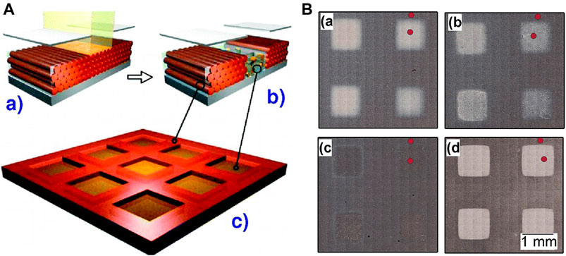
FIGURE 1. On the left (A), scheme of the preparation of mesoporous and mesostructured patterns in silica films. (a) the mesostructured films are irradiated with UV light through a mask. (b) The area irradiated loses the order and becomes mesoporous. (c) Mesotrusctured and mesoporous areas are generated. Reprinted with permission from Innocenzi et al. (2008). Copyright © 2008 American Chemical Society. On the right (B), optical images of mesostructured mesoporous films prepared by masked deep-UV exposure (a). The films were developed 10, 85 and 3,600 s in NaOH solution (b and c,d). The red dots mark the spots at which the films were characterized by FTIR spectroscopy and image ellipsometry. Reprinted with permission from Dattelbaum et al. (2003). Copyright © 2003 American Chemical Society.
Despite advantages of UV patterning for full-inorganic layers, this process requires long exposition times, over 120 min. Therefore, it is not unexpected that most of the publications based on direct UV sol-gel patterning involve hybrid organic-inorganic materials such as ORMOSILs (Janotta et al., 2003b) and ORMOCERs (Schmidt and Popall, 1990) with polymerizable functional groups. This approach was develop simultaneously to UV processing of all-inorganic layers by Schmidt´s and Minami´s groups as an alternative able to increase thickness of the layers and to increase their condensation rate (Tohge et al., 1988; Schmidt and Popall, 1990). This strategy was repeated in the following years by several groups. Innocenzi et al. introduced 3-glycidoxypropyltrimethoxysilane to substitute the more widely use 3-methacrloxypropyltrimethoxysilane (Brusatin et al., 2006). Characterization of such layers includes comparison of UV polymerization to thermal polymerization and the evolution of mechanical properties after photopolymerization (Soppera et al., 2005). Transition metal oxide precursors were incorporated to silica-based hybrid sols several times to tune the refractive index of the layers. In this regard, Yamada et al. worked with inorganic–organic hybrids including titanium oxide precursors, where the hybrid films have been synthesized from diethoxydimethylsilane and titanium ethoxide modified with ethyl acetoacetate (Yamada et al., 1999). Ayras et al. developed an alternative based on doped 3-methacryloxypropyl trimethoxysilane with zirconia precursor while Kang et al. based their strategy on the analogous titania precursor (Äyräs et al., 1999; Kang et al., 2013). Transmission and absorption of light in these ORMOCERs layers were studied first by Saavedra and later by Innocenzi (Yang et al., 1994; Costacurta et al., 2007). Due to the promising performance of such layers in the VIS-NIR, low losses, and easy processing, this material has been recommended and tested for photonic applications (Righini and Pelli, 1997; Costacurta et al., 2007).
Further improvement in terms of cost, time and pattern resolution was reached with laser writing processes. The direct laser technique applied to hybrid sol–gel films has the advantage of being mask-less, allowing rapid and simple prototyping comparable with mask-less photolithographic techniques. In addition, the direct laser writing can be tuned by adjusting independently the focus conditions, the laser irradiation, the writing beam power, and the scan speed, enabling microfabrication of various devices for optics and photonics (Righini and Pelli, 1997; Yamada et al., 1999; Costacurta et al., 2007).
Patterning With High Energy Radiation
Alternatively to the use of hybrid sol-gel layers, the exposure to higher energy sources such as soft X-ray (λ <1 nm), hard X-ray (λ < 0.5 nm), and electron beam (λ < 0.1 nm) proved itself convenient to reduce patterning times of all inorganic layers without additional resist, photoinitiator, or any chemical modification. Synchrotron X-ray or e-beam lithography decreased significantly the processing time and simultaneously provided higher resolution and reduced the side wall roughness. These advantages overcome most of UV pattering restrictions on all inorganic layers, limiting the use of UV irradiation patterning to hybrid inorganic-organic materials or ORMOSILs. The chemical reactions involved in the consolidation process induced by higher energy sources remain similar to the one described for UV radiation; a higher formation of free radicals increase condensation and complete hydrolysis of the unreacted alkoxides precursors, therefore encouraging densification on a very short time scale.
Different light sources may differ in the penetration depth of the beam, the exposure time requirements, the achieved aspect ratio, resolution, and focusing power (Levy and Zayat, 2015). Electron beam nanolithography patterning features have been reported down to sub-10 nm with an aspect ratio of 4 (Figure 2A) (Della Giustina et al., 2009; Brigo et al., 2012). Proximity X-ray lithography has been performed on hybrid films using a synchrotron source, achieving a resolution below 200 nm (Figure 2B) (Della Giustina et al., 2007). Regarding penetration depth, soft X-Ray does not allow full curing of very thick hybrid layers, which is possible with hard X-rays, but there is the advantage that the films can be written using a very well-focused beam to obtain patterns with high resolution at the nanoscale (Levy and Zayat, 2015).
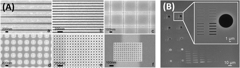
FIGURE 2. (A) phenyl-bridged polysilsesquioxane (ph-PSQ), for use as a new high resolution resist for electron beam lithography. Reprinted from Brigo et al. (2012), Copyright (2012), with permission from Elsevier. (B) Examples of high resolution features (less than 100 nm). Reprinted from Della Giustina et al. (2007), Copyright (2007), with permission from Elsevier.
Additionally to the extent of condensation, decomposition of organic molecules upon radiation needs to be accounted for (Innocenzi et al., 2012). Radiation damage either modifies the functional groups or removes the organic species depending on the radiation source, the intensity, and the exposure time (Werst and Vinokur, 2001). In the case of templated or hybrid films, hard X-ray exposures have been used to produce the decomposition of organic functional groups through the formation of radical species (Innocenzi et al., 2014).
In most of the cases discussed so far, sol-gel layers resemble a negative resist due to higher condensation rates and polymerization (Rantala et al., 1999; Visovsky et al., 2002). However, selective decomposition of organic material may enable these layers to behave as a positive resist, depending on their composition and structure (Grenci et al., 2011). Exposed regions may become fragile, hydrophilic and/or susceptible to silica etching agents.
Printing and Imprint Lithography
Besides photolithography and electron beam lithography, several additional techniques, not available to pattern hard layers, become available by taking advantage of the soft nature of sol-gel layers at the initial steps. These techniques include scanning probe lithography [micro-pen lithography and dip-pen lithography Figure 3A and Figure 4C (Su et al., 2002)] and imprint lithography [Gravure printing Figure 3B (Herzog et al., 2019), micro melding, micro contact printing (Jeon et al., 1995; Äyräs et al., 1999), stamper (Tohge et al., 1988), or inkjet printing Figure 4A and Figure 4B (Mougenot et al., 2006; Fousseret et al., 2010)]. Although most of them were developed for some specific materials, the possibility to use sol-gel solutions as an ink (Duoss et al., 2007) opens sol-gel chemistry the door to a wide variety of processes, which provide several advantages such as lower cost, suitability for applications in biotechnology and plastics, and compatibility with large or nonplanar (non-flat) surfaces. These techniques cover a wide range of pattern sizes from tens of nanometers to micrometers and present different limitations or benefits. The main limitation of soft lithography is the slow processing time, which can be overcome by micro-pen lithography or ink-jet printing. The former is suitable to produce patterned macroscopic arrays of discrete structures, while the latter is better adapted to write continuous patterns.
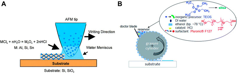
FIGURE 3. Schematics for dip-pen nanolithography (A) and gravure printing (B) based on sol-gel inks. Reprinted with permission from Su et al. (2002), copyright © 2002 American Chemical Society. Permission from Herzog et al. (2019) was granted, published by The Royal Society of Chemistry.
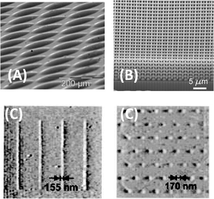
FIGURE 4. (A) SEM images of 25-layer inkjet printed microdot arrays realized from a sol aged 48hs and in situ functionalized with 5 mol% MPTES and 5 mol% TFTS. Reprinted with permission from Fousseret et al. (2010). Copyright © 2010 American Chemical Society. (B) Focused ion beam (FIB)-milled cross-section of direct ink writing 3D calcined TiO2 structure heated to 715°C. Reproduced with permission from Duoss et al. (2007). Copyright © 2007 WILEY-VCH Verlag GmbH and Co. KGaA, Weinheim. (C) Topographic AFM image of composite tin oxide/P-123 nanostructures on silicon oxide, dot array of aluminum oxide/P-123 composite nanostructures formed on silicon. Reprinted with permission from Su et al. (2002), copyright © 2002 American Chemical Society.
Sol-Gel Claddings for Sensing in Photonic Devices
Parallel to the development of sol-gel layers as a constituent material for the fabrication of waveguides or dot arrays, sol-gel layers were engineered as claddings for sensing purposes. The possibility to develop appropriate molecular recognition layers serving as solid-phase enrichment matrix for analyte molecules, while simultaneously excluding undesirable molecules, i.e., sources of interference, has been a strategy adopted in a large number of chemical sensing devices (opto-chemical, electro-chemical, plasmonic) (Boulart et al., 2008; Brassard et al., 2012; Mateescu et al., 2012; Bliem et al., 2018). In particular, molecular recognition layers became of utmost importance for highly sensitive transducers with low selectivity and specificity such as refractive index based waveguide sensors (Dullo et al., 2015; Beneitez et al., 2016). In this regard, polymers have been the first material of choice due to their easy processing and their behavior as extraction materials, with the enrichment properties mainly dependent on their polarity, pore size, and pore distribution (Stach et al., 2015). Nevertheless, these materials present thermal, mechanical and chemical limitations. They are thermally labile, many of them with glass transition temperatures below 100°C, and their Young modulus is measured in megapascals meaning that they are susceptible to structure modifications under small temperature and pressure variations. Polymers deteriorate upon exposure to high energy radiation and many of them can´t sustain acid or alkaline media as well as oxidative chemicals.
Sol-gels as alternatives to organic polymers are equally capable of providing specificity to custom analytical tasks, while they exhibit advantageous optical, dielectric, thermal, and acoustic properties (Scott et al., 2001; Bhatia et al., 2005; Lionello et al., 2017; Zelcer et al., 2019). Sol-gel materials withstand high temperatures and rigorous chemical conditions, making them highly suitable as sensor recognition elements operating under harsh environmental conditions (Fuertes and Soler-Illia, 2006; Alberti et al., 2019). A major advantage of sol-gel technology is in its tunable chemical properties, its control over polarity, porous volume and pore size (Soler-Illia et al., 2003). Furthermore, the introduction of organically modified silanes through co-condensation or post-grafting modification allows for incorporation of reactive functional groups into the sol-gel claddings enabling specific recognition sites and addressable partition coefficients (Otal et al., 2006).
Claddings on ATR Crystals
The sol-gel claddings found their first practical example on Attenuated Total Reflection (ATR) for CO detection in 1992 (Dulebohn et al., 1992). ATR can be seen as the first generation of evanescence wave spectroscopy and the predecessor of nowadays fiber optics and on-chip waveguide spectroscopy. Being widely distributed and used for the characterization of materials and samples as a routine technique, ATR crystal configuration is very attractive to test enrichment layers for sensing purposes. Some years after the first demonstration, hydrophobic sol-gel claddings were deposited on ATR crystals for spectroscopy sensing of low concentration of benzene in water (Lu et al., 1996). In this work, no templating agent was used and a post grafting procedure was employed to further functionalize the thin film. An average pore size was estimated to be 29 Å, and the porosity was estimated to be 30%. Compared to sensors prepared using organic polymer films, the porous sol-gel coated sensors have much lower diffusion resistance and improved the sensor response time to less than 6 s. This approach simultaneously kept water away from interacting with the evanescent field, and, therefore, reduced one of the main interferences in MIR spectroscopy. A similar strategy was followed by Mizaikoff’s group taking advantage of sol-gel hybrid thin layer preconcentration capability and hydrophobicity to develop a cladding for the detection of organophosphate pesticides in water samples on ATR (Janotta et al., 2003b). This approach proved itself appropriate for preconcentration of the analyte of interest, improved the figures of merit and facilitated the limit of detection down to sub-ppm levels. The layers didn’t exhibit any changes in their performance within repeated trials in two consecutive days. Interestingly, porosity was not evaluated and higher sensor response time, between 24 and 200 min, was needed to achieve the claimed sensitivity (Figures 5A,B). Surprisingly, this approach was not further investigated until recently by Baumgartner et al. (Baumgartner et al., 2018). The group deposited a mesoporous silica coating on an ATR crystal for the determination of benzonitrile and valeronitrile from a water matrix (Figure 6A). Hydrophobicity was attained by simultaneous template removal and functionalization in acetone. A similar approach was used for the determination of toluene, p-xylene and trimethylbenzene from water vapor two years later by the same group (Baumgartner et al., 2020b) (Figures 5C,D). In this case, samples were calcinated to 400°C and a postgrafting step was done in toluene. The group has worked intensively in recent years on silica mesoporous coatings to increase it applicability to new target molecules. Templated silica thin layers were calcinated and subsequently functionalized with a cationic silane to increase the amount of nitrate on the layer and therefore decrease the detection limit (Baumgartner et al., 2020a), A decrease in the enrichment capacity of the layer was noted withing two week period and attributed to instability of the films and leaching of the silane without further experiments. Although functionalized mesoporous silica samples, as reported elsewhere (Fontecave et al., 2012), showed increased stability in aqueous environments in comparison to bare mesoporous silica, the stability of mesoporous silica has been proven to be susceptible to degradation, particularly under biological conditions as it has been reviewed recently (Alberti et al., 2019). Therefore, this issue should be kept in mind for future applications.
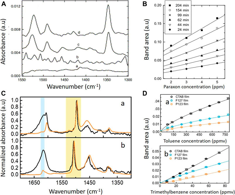
FIGURE 5. A) Response produced after 60 min by ZnSe waveguide sensors mounted in a flow-through cell to the organophosphate parathion.: (a) uncoated waveguide purged with 2.5 ppm parathion; (b) a Teflon AF coated waveguide purged with 2.5 ppm parathion; (c) uncoated waveguide purged with 40 ppm parathion; (d) sol–gel coated waveguide purged with 2.5 ppm parathion. (B) Calibration curve of paraoxon over the concentration range of 2–5 ppm evaluated at different times during the absorption process. Reprinted from Janotta et al. (2003b), Copyright (2003), with permission from Elsevier. (C) FTIR spectra (normalized to a peak absorbance of 1 of toluene (a), and 1,2,4-trimethylbenzene (b) obtained after enrichment into the mesoporous silica film synthesized using CTAB (black curves) and for the pure substance on a commercial ATR unit (orange spectra). Bands of adsorbed water are highlighted in blue and the spectral region of interest with skeletal ring vibrations of toluene at 1,496 cm−1 and 1,2,4-trimethylbenzene at 1,506 cm−1 is highlighted in yellow. (D) Adsorption isotherms of different mesoporous films for (a) toluene, and (b) 1,2,4-trimethylbenzene. Reprinted from Baumgartner et al. (2020b), Copyright (2020), with permission from Elsevier.
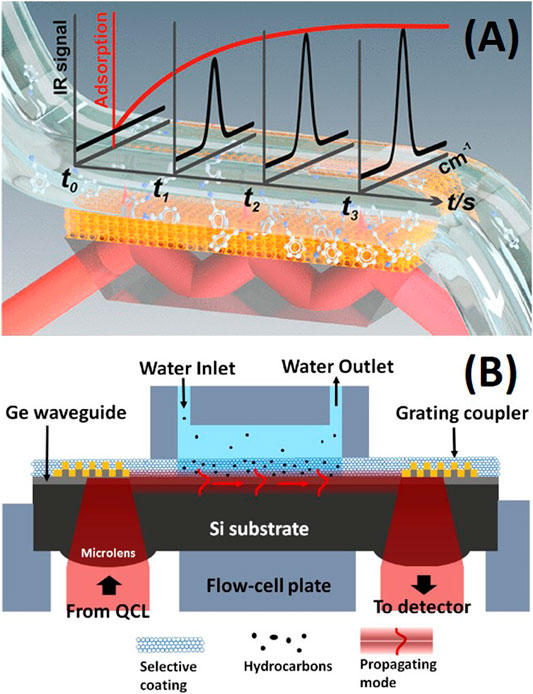
FIGURE 6. (A) Hybrid porous cladding over ATR crystal for benzonitrile sensing. Reprinted with permission from Baumgartner et al. (2018) Copyright © 2018 American Chemical Society. (B) Schematic illustrating the sensing platforms used by Beneitez et al. Hybrid porous cladding on top a single mode waveguide. Reproduces with the authors permission from Benéitez et al. (2020).
Claddings on Fiber Optics
The extended use of ATR configuration for testing enrichment coatings finds its explanation in its simplicity, stability, availability and ideal compatibility to probe both liquid and vapors, even under flow. The low volume of interaction between the sample and the evanescence field helps to avoid saturation of the signal by the matrix and therefore enables the use of non-transparent liquid samples and coatings. Nevertheless, this advantage has become the main limitation to sensitivity, hindering applications when the analyte molecules are scarce, e.g. in gas sensing. To boost sensitivity, the interaction volume can be improved substantially by the use of fiber optics and integrated waveguides, considered respectively as the second and third generation of evanescence wave spectroscopy (Jeronimo et al., 2007). Additionally, the use of fiber optics opened the possibility for the design of refractive index based sensors, a strategy that would be later applied to on-chip devices (Kozma et al., 2014). Although we will not go deep into the topic of fiber sensing, its development has been in close relation with the development of sol-gel claddings and it is worth to be mentioned as most of the sol-gel coatings applied to fibers have their corresponding analog over ATR and have been recently applied to on-chip systems. To exemplify this point we can describe briefly the work done by Mizaikoff’s, Pang’s and Fangs’s groups. The former tested the same sol-gel silica based coating on both fibers and ATR crystals in 2003 (Janotta et al., 2003a). In this case, organically modified sol-gels as recognition membranes were demonstrated for in situ detection of nitro-based aromatic compounds in aqueous media. In a similar way, a sol-gel hybrid layer has been deposited on fiber gratings and on ring resonators for the development of ethanol vapor sensing the same year by Gu and Xu, and Pang´s groups respectively (Gu and Xu, 2007; Pang et al., 2007). Since the introduction of sol-gel claddings on optical fibers originally by MacCraith for pH sensing and for oxygen detection, numerous amount of work has been published in the field soon after (Maccraith et al., 1991; MacCraith et al., 1993). Details on optical fibers for sensing applications can be found in several reviews e.g., by Marazuela, Mizaikoff, and Orellana (Marazuela and Moreno-Bondi, 2002; Mizaikoff, 2003; Orellana and Haigh, 2008).
Claddings on Integrated Waveguides
The use of sol gel claddings over integrated waveguides came as the third generation of evanesce wave sensing and was also implemented as a strategy in refractive index sensitive devices such as directional couplers, interferometers, or ring resonators. As opposed to classical ATR configuration, in waveguides the light-matter interaction takes place along the whole waveguide length that is in contact with the analyte and not only at discrete locations. This leads to higher effective path-lengths and thus to higher sensitivity. This approach can only be applied to waveguides with extended water background suppression, which facilitates the detection of analyte molecules due to increased discrimination capability against interfering backgrounds.
In 1995, Yang and Saavedra reported a sol-gel cladding deposited on a multimode planar waveguide as the first logical step toward the use of single mode waveguides that came to light more than 20 years later. The Pb2+ and pH sensor that was the subject of this work was based on immobilized xylenolorange and bromocresol purple in a sol-gel indicator layer, respectively. These layers were placed as a cladding over a silica-titania sol-gel-based waveguide layer. The authors claim this cladding layer remains porous to the analyte and defined this material as “undensified glass” with low refractive index of 1.414 (Yang and Saavedra, 1995). Saavedra’s group worked intensively with ORMOSIL layers and reported the detection of gaseous iodine one year later (Yang et al., 1996). The sensing principle in this case was based on light absorption at 488 nm, characteristic for a charge transfer complex formed between the iodine and phenyl groups that have been covalently incorporated into the sol-gel hybrid indicator film. In another work, MacCraith developed a fluorescent sol-gel coating over a planar waveguide able to capture the fluorescence (Gouin et al., 1998). They used this platform for oxygen sensing based on fluorescence quenching.
Sol-gel-based layers over single mode waveguides for spectroscopy were only published in the last couple of years. Inspired by previous reports on ATR crystals, similar coatings have been recently tested on single mode waveguides for Raman and absorption spectroscopy. Haolan Zhao et al. reported a VOC sensing chip based on silicon nitride waveguides for Raman spectroscopy (Zhao et al., 2020). Here, they followed the same coating protocol applied on ATR crystals for determination of benzonitrile and valeronitrile from a water matrix as in (Baumgartner et al., 2018) (Baumgartner et al., 2020b). An even more recent report described an hydrophobic mesoporous silica coating spin-coated on germanium waveguide structures for measuring toluene in water following the same idea proposed by Lopez and Brinker in 1996 on ATR crystals (Figure 6B) (Benéitez et al., 2020).
As for refractive index sensors, Pang and co-workers develop a ring resonator with a sol gel cladding sensitive to ethanol (Pang et al., 2007). The authors expected the inherent microporosity of the synthesized layer to absorb vapor molecules, in particular ethanol due to the presence of alkoxides in the synthesis procedure. Yebo et al. used platinum (Pt)-doped sol-gel tungsten oxide coating as a hydrogen-sensitive element over a ring resonator (Yebo et al., 2009). The catalyst boosts hydrogen oxidation rate selectively with the corresponding release of heat, which produces a change in the refractive index that is sensed by the ring resonator. A sol-gel layer was also used as an upper cladding of a micro ring resonator for water vapor sensing, based on the increase of the refractive index of the cladding upon water absorption (Bhola et al., 2009). The use of microring resonators with a selective coating was again used by Yebo three years later. In this new work, a nano-porous aluminosilicate coating for ammonia sensing was reported, which results in a reversible response to NH3 with selectivity relative to CO2 (Yebo et al., 2012). Also taking advantage of refractive index change, Baets’ group and Steenberge´s group used another two alternative approaches. The former one designed a Mach-Zehnder interferometer having one sol-gel coated arm exposed to gas vapors. They were able to retrieve a limit of detection of 65 ppb, 247 ppb, and 1.6 ppb for acetone, isopropyl alcohol, and ethanol, respectively (Antonacci et al., 2020). The latter, implemented a Bragg grating covered with a commercially available hybrid material and was used for developing a temperature sensor (Beneitez et al., 2016).
Sol-Gel Waveguides
Planar Sol-Gel Waveguides
Simultaneously with the development of sol-gel-based claddings as recognition layers to increase sensitivity, the sol-gel chemistry found its use in the processing of planar waveguide core layers, as an alternative to CVD, PVD, PCVD, or sputtering. The motivation was once again its low cost, versatility (i.e. tuneable refractive index), and simplicity of deposition (i.e. spin coating, dip coating). Originally, these layers were engineered to guide light and not to provide for enrichment, therefore all-inorganic non-porous layers were targeted due to their higher refractive index. The firsts reports using sol-gel layers as planar waveguides can be traced back to the 70′ and 80´ (Ulrich and Weber, 1972; Herrmann and Wildmann, 1983; Hewak and Lit., 1988). Nevertheless, sol-gel thin film planar waveguides for specific sensing applications started to be tested widely only at the beginning of 90′s. The original material used for this purpose was a mix-inorganic oxide between silica and titania introduced in 1983. Titanium oxide firstly and zirconium dioxide later were used as dopants to increase the refractive index of silica and therefore work as planar waveguides over silica substrates. Titanium dioxide as a dopant was further described in 1988 and rediscovered in 2013 (Boudrioua, 2013), while zirconium oxide properties for integrated optics were described early this century by Flory´s group (Elalamy et al., 2004). These materials were used continuously in the following years, and became commercially available for optical waveguide spectroscopy applications by Zeptosens and Microvacuum Ltd. Over time, additional oxides such as wolframium oxide and tin oxide were incorporated to the companies’ catalog. These materials presented very low losses down to 0.3 dB/cm in the visible range. Grandin and co-workers have used these layers to develop a new tool known as waveguide excitation fluorescence microscopy. This technique can provide images with high spatial resolution combined with dynamic sensing of biomolecular interactions (Grandin et al., 2006). A very interesting work done by Martinelli’s group, uses pure inorganic layers of both titanium oxide and zirconium oxide for evanescent wave excitation of microarrays for bio sensing and potential application in fluorescence microscopy (Bedu et al., 2010).
The possibility to dope sol-gel-based thin films has not only allowed to tune the refractive index by modifying the ratio between different inorganic oxides, but has additionally enabled the fabrication of composite materials or sophisticated doped inorganic layers with outstanding properties not easily accessible by other means. One major strategy is the inclusion of fluorescent compounds in the core of waveguide sensing devices. Edmiston and Saavedra used uranium oxide as a photo-bleaching resistant fluorescent dopant for sensing horse heart cytochrome c (Edmiston and Saavedra, 1997). Sol-gel materials doped with rare-earth elements such as Eu, Er, Nb were studied by Biwas’ group and Orignac’s group for potential applications in integrated lasers and amplifiers (Orignac et al., 1996; Biswas et al., 2000). The second example is based on doping the sol with rare-earth elements aimed for the fabrication of thin layers for up-conversion purposes (Bahtat et al., 1996).
However, the use of pure inorganic layers limits the dopants to high temperature resistant moieties, ruling out the possibility to implement this approach for organic molecules. This inconvenience has been circumvented by the use of low temperature sol-gel processes based on organically modified sol-gel layers. In this case, the precursors are not fully inorganic, but also have some organic components that make the gel network more flexible and less prone to cracking during sintering. These planar waveguides have appeared as an intermediate option between inorganic sol-gel materials and polymer planar waveguides. Among other precursors, methyltrietoxysilane or Poly-dimethylsiloxane were used as partial or total substitution of tetraethyl orthosilicate (TEOS) in the starting solution frequently doped with ZrO2 or TiO2 (Yang et al., 1994). Alternatively, polymerizable molecules such as γ-glycidyloxypropyl trimethoxysilane (GPTMS)/γ-methacryloxypropyl trimethoxysilane (MPTMS) have been reported by Schmidt, Sorek, Innocenzi and many others (Schmidt and Popall, 1990; Sorek et al., 1993; Costacurta et al., 2007). Zirconia-based ORMOSIL planar waveguides with different ZrO2 content were produced by a low temperature sol-gel process by Giorgetti et al. (Giorgetti et al., 1999). Propagation losses as low as 0.5 dB/cm or less were found at 488 nm for films with low ZrO2 content and the feasibility of organic dye doping of the films for active waveguides was also demonstrated. Nevertheless, most of these active layers have still been used as coating layers over traditional materials (Maccraith and Mcdonagh, 2002) and not directly as waveguides themselves. The stability of the signal and the performance of such layers over time has been mostly overlooked in the recent publications and stability of the films should be tracked down to detailed condensation and aging analysis of the layers done in previous reports: The effect of X-ray dose and UV-radiation have been described by Innocenzi group for TEOS-methyltrietoxysilane (MTES) and TEOS-MPTMS respectively (Costacurta et al., 2007; Jiang et al., 2016); Phenyltrimethoxysilane-Tetramethoxysilane curing process has been monitored through FTIR measurements by Mizaikoff’s group (Janotta et al., 2003a). The composition and the polymerization methods followed will be determinant on the final characteristics and long-term performance of the layers.
Single-Mode Sol-Gel Waveguides
The development of lithography processes to pattern directly and indirectly sol-gel thin films built up the foundation for fabrication of single mode sol-gel based waveguides. In comparison to planar structures, single mode waveguides improve the signal to noise ratio by increasing transmitted signal levels and avoiding multimode interference. They also enable the fabrication of longer pathlengths on smaller footprints. Although, as discussed previously, sol-gel-based materials provide a wide palette of patterning options to select from, most of reports use ORMOSIL and UV lithography due to its accessibility, low cost, and its ease and swiftness of fabrication. The first low-loss single mode integrated optical device published in 1995 (Li et al., 1995) was based on an organic modified sol-gel silica glass. The group proposed a directional coupler as an example of the first fabrication of a silica glass integrated optic device by simple UV-light imprinting. Channel waveguides (surface, ridge, and buried waveguides) and gratings on hybrid materials were reported in the last years of 90′s decade by Najafi et al. The group reported waveguides with a width as small as 2 μm and losses of 0.1 dB/cm for 1.55 μm wavelength (Najafi et al., 1998). Exposure of the sol-gel to the UV-light sensitizes the vinyl monomer substituent to polymerization, filling voids in the glass and raising the refractive index in the region defined by the mask. A similar strategy was used by Coudray et al. (Coudray et al., 1996) for a power splitter and the fabrication of waveguides to study the losses of the material at 1.55 μm (Coudray, 1997). Enami et al. (Enami et al., 2007) designed a Mach-Zehnder modulator, in which both the cladding and the core consist of a widely used precursor for hybrid materials, methacryloyloxy propyltrimethoxysilane (MAPTMS) and an index modifier, zirconium propoxide. All-inorganic directional couplers were fabricated through conventional photoresist and ammonia fluoride wet chemical etching of a sol–gel derived silica–titania (SiO2:TiO2) layer several years later by Cuma Tyszkiewicz et al. (Tyszkiewicz et al., 2016).
The versatilile sol–gel derived silica–titania (SiO2:TiO2) material developed through years become the material of choice for manufacturing 3D structures such as 3D ring resonator with the highest Q factor reported so far for UV-curable integrated micro-ring resonators (Figure 7) (Bar-on et al., 2018). The process is based on a novel dual-step soft nanoimprint lithography for producing devices with smooth surfaces, combined with fast sol-gel technology providing highly transparent materials.
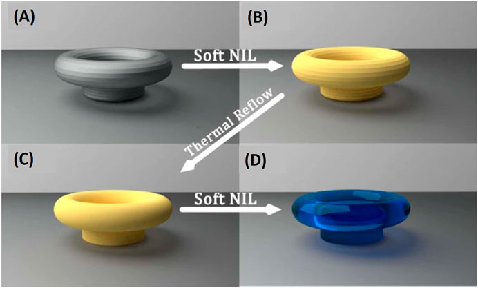
FIGURE 7. Dual-step soft nanolithography. (A) Master device fabricated using DLW made of cross linked SU-8 (gray). (B) First soft NIL step -Replication of the master device into non-crosslinked SU-8 (yellow). (C) Reflow replica from non-crosslinked SU-8 (Yellow). (D) Second soft NIL step–replication of the reflowed resonator into sol-gel (blue). Reproduces from Bar-on et al. (2018), open access article distributed under the terms of the Creative Commons CC BY license.
Although waveguide design based on sol-gel materials is moving forward constantly, only a few examples of sol-gel single-mode waveguides applied to sensing applications have been published. Lingyun Jia group have utilized a sol−gel system to fabricate micro ring resonator biosensors (Ren et al., 2013). This study presents a sol−gel material system based on three precursors, phenyl trimethoxysilane, methyl trimethoxysilane and 3-(methacryloxy) propyl trimethoxysilane. The fabricated ring resonators play the role of both optical transducers and carriers for receptor proteins, which were adsorbed to the sol-gel material without any physical or chemical modification. Bearman et al. submitted a patent (Bearman and Cohen, 2006) for the fabrication of a biosensor based on research performed by Yamanaka et al. (Yamanaka et al., 1992). The biosensor includes a ring interferometer representing the sensing volume, a laser for supplying light to the ring interferometer, and a photodetector. The sensing volume is characterized by having an array of pores sized for immobilizing bio-receptors, which bind the targeted analyte. The binding process changes the index of refraction of the sensing volume. Unfortunately, no experimental information is provided. Another patent application from Sensorhut ltd. from 2015 (Hutter, 2015) mentioning sol-gel layers encourages the use of porous materials for the use in spectroscopy, however, this group worked exclusively with porous silicon.
These above works suggest an increased interest in the topic, but ignore several challenges that need to be addressed to allow for practical applications. In this regard, a recent report by the authors describes an all-inorganic mesoporous sol-gel single mode rib-waveguide for gas sensing by laser absorption spectroscopy. The pore network allows the diffusion of molecules promptly into the core material enabling the interaction of the electric field with the targeted molecule directly in the waveguide core and without the need for a cladding (Datta et al., 2021). Despite the encouraging result, absorption and interference with water present in the pore network is compromising the specificity and the detection limit.
Outlook and Future Perspectives
Current trends in waveguide-based sensors take advantage of waveguides as active transducers, generating the actual analytical signal by ensuring reproducible interaction between the light and the analyte (i.e., conversion of chemical, biochemical, or biological processes or recognition events into changes of optical properties). The use of sol-gel chemistry for the realization of such sensors has developed simultaneously in two different dimensions: as a constituent material for planar and single mode waveguides for traditional applications without any recognition or preconcentration properties, and as functional claddings. The former aimed toward the fabrication of low loss waveguides with very little attention paid to its application in sensing. The latter, on the contrary, developed consciously and systematically toward increasing analyte concentration (enrichment), specific recognition of analytes, and suppression of interferences.
All-inorganic sol-gel materials were first developed as a constituent material for photonic applications in planar waveguides and successfully developed into commercially available products for sensing. The use of all-inorganic sol-gel layers, however, has been in many cases replaced due to the availability of alternative deposition techniques such as sputtering, CVD or PCVD. The impact of sol-gel chemistry has been leveraged in the latest years by the use of hybrid inorganic-organic layers. These materials can exhibit microporosity defined by a non-compact polymeric network and a high versatility in doping and functionalization, without the need for high temperature treatment. Additionally, these hybrid layers have been engineered to be directly patternable without the use of additional photoresist in a matter of minutes under exposure to UV light. The importance of these new materials and processes has been exemplified on recently fabricated sol-gel single mode waveguides and 3D ring resonators with record-low losses and outstanding optical properties. The combination of micrometer scale structures arising from the top down techniques with the versatility of functionalization, doping, and nanostructuring of these materials arising from bottom up techniques, gives sol-gel waveguides a great perspective for the future. The field has grown and matured steadily in the last decades and continuous collaboration between analytical chemistry, photonics, and the (bio)sensing community will be the key to steer the future development of sol-gel nanophotonic devices toward real-world applications.
Author Contributions
SA reviewed the literature and composed the manuscript. JJ contributed to the writing, provided critical feedback and helped to organize the manuscript.
Funding
This work was supported by the European Research Council (ERC) Staring Grant no. 758973.
Conflict of Interest
The authors declare that the research was conducted in the absence of any commercial or financial relationships that could be construed as a potential conflict of interest.
References
Alberti, S., Soler-Illia, G. J. A. A., and Azzaroni, O. (2015). Gated supramolecular chemistry in hybrid mesoporous silica nanoarchitectures: controlled delivery and molecular transport in response to chemical, physical and biological stimuli. Chem. Commun. 51, 6050–6075. doi:10.1039/C4CC10414E
Alberti, S., Steinberg, P. Y., Giménez, G., Amenitsch, H., Ybarra, G., Azzaroni, O., et al. (2019). Chemical stability of mesoporous oxide thin film electrodes under electrochemical cycling: from dissolution to stabilization. Langmuir 35, 6279–6287. doi:10.1021/acs.langmuir.9b00224
Antonacci, G., Goyvaerts, J., Zhao, H., Baumgartner, B., Lendl, B., and Baets, R. (2020). Ultra-sensitive refractive index gas sensor with functionalized silicon nitride photonic circuits. APL Photonics 5, 081301. doi:10.1063/5.0013577
Äyräs, P., Rantala, J. T., Honkanen, S., Mendes, S. B., and Peyghambarian, N. (1999). Diffraction gratings in sol-gel films by direct contact printing using a UV-mercury lamp. Optic Commun. 162, 215–218. doi:10.1016/S0030-4018(99)00108-X
Bahtat, A., Bouazaoui, M., Bahtat, M., Garapon, C., Jacquier, B., and Mugnier, J. (1996). Up-conversion fluorescence spectroscopy in Er3+: TiO2 planar waveguides prepared by a sol-gel process. J. Non-Cryst. Solids 202, 16–22. doi:10.1016/0022-3093(96)00172-X
Bar-on, O., Brenner, P., Siegle, T., Gvishi, R., Kalt, H., and Lemmer, U. (2018). High quality 3D photonics using nano imprint lithography of fast sol-gel materials. Sci. Rep. 8, 1–7. doi:10.1038/s41598-018-26261-3
Baudet, E., Gutierrez-Arroyo, A., Baillieul, M., Charrier, J., Němec, P., Bodiou, L., et al. (2017). Development of an evanescent optical integrated sensor in the mid-infrared for detection of pollution in groundwater or seawater. Adv. Device Mater. 3, 23–29. doi:10.1080/20550308.2017.1338211
Baumgartner, B., Freitag, S., Gasser, C., and Lendl, B. (2020a). A pocket-sized 3D-printed attenuated total reflection-infrared filtometer combined with functionalized silica films for nitrate sensing in water. Sensor. Actuator. B Chem. 310, 127847. doi:10.1016/j.snb.2020.127847
Baumgartner, B., Hayden, J., and Lendl, B. (2020b). Chemical Mesoporous silica films for sensing volatile organic compounds using attenuated total reflection spectroscopy. Sensor. Actuator. B Chem. 302, 127194. doi:10.1016/j.snb.2019.127194
Baumgartner, B., Hayden, J., Schwaighofer, A., and Lendl, B. (2018). In Situ IR spectroscopy of mesoporous silica films for monitoring adsorption processes and trace analysis. ACS Appl. Nano Mater. 1, 7083–7091. doi:10.1021/acsanm.8b01876
Bearman, G., and Cohen, D. (2006). Ring-interferometric sol-gel bio-sensor. California Institute Of Technology, California, United States Patent No. US7019847B1 7 (019), 8.
Bedu, M., Sagarzazu, G., Gacoin, T., Audebert, P., Weisbuch, C., and Martinelli, L. (2010). Sol-gel planar waveguides for improved fluorescence microarrays. Thin Solid Films 518, 4450–4457. doi:10.1016/j.tsf.2010.02.026
Benéitez, N. T., Baumgartner, B., Missinne, J., Radosavljevic, S., Wacht, D., Hugger, S., et al. (2020). Mid-IR sensing platform for trace analysis in aqueous solutions based on a germanium-on-silicon waveguide chip with a mesoporous silica coating for analyte enrichment. Opt. Express 28, 27013. doi:10.1364/OE.399646
Beneitez, N. T., Missinne, J., Shi, Y., Chiesura, G., Luyckx, G., Degrieck, J., et al. (2016). Highly sensitive waveguide Bragg grating temperature sensor using hybrid polymers. IEEE Photon. Technol. Lett. 28, 1150–1153. doi:10.1109/LPT.2016.2533020
Bhatia, S. K., Jepps, O. G., and Nicholson, D. (2005). Adsorbate transport in nanopores. Adsorption 11, 443–447. doi:10.1007/s10450-005-5965-9
Bhola, B., Nosovitskiy, P., Mahalingam, H., and Steier, W. H. (2009). Sol-gel-based integrated optical microring resonator humidity sensor. IEEE Sensor. J. 9, 740–747. doi:10.1109/JSEN.2009.2020113
Biswas, A., Friend, C. S., MacIel, G. S., and Prasad, P. N. (2000). Optical properties of Europium doped gels during densification. J. Non-Cryst. Solids 261, 9–14. doi:10.1016/S0022-3093(99)00653-5
Bliem, C., Piccinini, E., Knoll, W., and Azzaroni, O. (2018). Enzyme multilayers on graphene-based FETs for biosensing applications. Meth. Enzymol. 609, 23–46. doi:10.1016/bs.mie.2018.06.001
Bohannan, E. W., Gao, X., Gaston, K. R., Doss, C. D., Sotiriou-leventis, C., and Leventis, N. (2002). Photolithographic patterning and doping of silica xerogel films. J. Sol. Gel Sci. Technol. 23, 235–245. doi:10.1023/A:1013974915198
Boudrioua, O. B. A. F. A. (2013). Low optical loss nano-structured TiO2 planar waveguides by sol - gel route for photonic crystal applications. doi:10.1007/s11082-013-9692-2
Boulart, C., Mowlem, M. C., Connelly, D. P., Dutasta, J., and German, C. R. (2008). A novel, low-cost, high performance dissolved methane sensor for aqueous environments. Opt. Express 16, 12607. doi:10.1364/OE.16.012607
Brassard, J.-D., Sarkar, D. K., and Perron, J. (2012). Fluorine based superhydrophobic coatings. Appl. Sci. 2, 453–464. doi:10.3390/app2020453
Briano, F. O., Errando-herranz, C., and Gylfason, K. B. (2020). On-chip dispersion spectroscopy of CO2 using a mid-infrared microring resonator,” in CLEO: Science and Innovations 2020, Washington, United States, May 10–15, 2020, 1–2.
Briche, S., Tebby, Z., Riassetto, D., Messaoud, M., Gamet, E., Pernot, E., et al. (2011). New insights in photo-patterned sol-gel-derived TiO2 films. J. Mater. Sci. 46, 1474–1486. doi:10.1007/s10853-010-4949-7
Brigo, L., Auzelyte, V., Lister, K. A., Brugger, J., and Brusatin, G. (2012). Phenyl-bridged polysilsesquioxane positive and negative resist for electron beam lithography. Nanotechnology 23, 325302. doi:10.1088/0957-4484/23/32/325302
Brinker, C. J., and Scherer, G. W. (2013). Sol-gel science: the physics and chemistry of sol-gel processing. Cambridge, MA: Academic Press.
Brusatin, G., Della Giustina, G., Guglielmi, M., and Innocenzi, P. (2006). Photocurable glycidoxypropyltrimethoxysilane based sol-gel hybrid materials. Prog. Solid State Chem. 34, 223–229. doi:10.1016/j.progsolidstchem.2005.11.005
Costacurta, S., Malfatti, L., Falcaro, P., and Innocenzi, P. (2007). Photocurable silica hybrid organic-inorganic films for photonic applications. J. Sol. Gel Sci. Technol. 44, 59–64. doi:10.1007/s10971-007-1594-y
Coudray, P., Chisham, J., Malek-Tabrizi, A., Li, C.-Y., Andrews, M. P., Peyghambarian, N., et al. (1996). Ultraviolet light imprinted sol-gel silica glass waveguide devices on silicon. Optic Commun. 128, 19–22. doi:10.1016/0030-4018(96)00101-0
Coudray, P. (1997). Ultraviolet light imprinted sol-gel silica glass low-loss waveguides for use at 1.55 μm. Opt. Eng. 36, 1234. doi:10.1117/1.601243
Datta, A., Alberti, S., Vlk, M., and Jágerská, J. (2021). “Sol-gel mesoporous layers for sensing applications,” in Conference on Lasers and Electro-Optics Europe & European Quantum Electronics Conference (CLEO/Europe-EQEC), Munich, Germany, June 20–24, 2021.
Dattelbaum, A. M., Amweg, M. L., Ruiz, J. D., Ecke, L. E., Shreve, A. P., and Parikh, A. N. (2005). Surfactant removal and silica condensation during the photochemical calcination of thin film silica mesophases. J. Phys. Chem. B 109, 14551–14556. doi:10.1021/jp051401+
Dattelbaum, A. M., Amweg, M. L., Ecke, L. E., Yee, C. K., Shreve, A. P., and Parikh, A. N. (2003). Photochemical pattern transfer and enhancement of thin film silica mesophases. Nano Lett. 3, 719–722. doi:10.1021/nl0341279
Della Giustina, G., Brusatin, G., Guglielmi, M., and Romanato, F. (2007). Direct nanopattern of hybrid sol-gel films. Mater. Sci. Eng. C 27, 1382–1385. doi:10.1016/j.msec.2006.09.032
Della Giustina, G., Prasciolu, M., Brusatin, G., Guglielmi, M., and Romanato, F. (2009). Electron beam lithography of hybrid sol-gel negative resist. Microelectron. Eng. 86, 745–748. doi:10.1016/j.mee.2008.12.044
Densmore, A., Xu, D.-X., Janz, S., Waldron, P., Lapointe, J., Mischki, T., et al. (2008). Sensitive label-free biomolecular detection using thin silicon waveguides. Adv. Opt. Technol. 2008, 1–9. doi:10.1155/2008/725967
Doshi, D. A., Huesing, N. K., Lu, M., Fan, H., Lu, Y., Simmons-Potter, K., et al. (2000). Optically defined multifunctional patterning of photosensitive thin-film silica mesophases. Science 290, 107–111. doi:10.1126/science.290.5489.107
Dulebohn, J. I., Haefner, S. C., Berglund, K. A., and Dunbar, K. R. (1992). Reversible carbon monoxide addition to sol-gel derived composite films containing a cationic rhodium(I) complex: towards the development of a new class of molecule-based carbon monoxide sensors. Chem. Mater. 4, 506–508. doi:10.1021/cm00021a006
Dullo, F. T., Lindecrantz, S., Jágerská, J., Hansen, J. H., Engqvist, M., Solbø, S. A., et al. (2015). Sensitive on-chip methane detection with a cryptophane-A cladded Mach-Zehnder interferometer. Opt. Express 23, 31564. doi:10.1364/OE.23.031564
Duoss, E. B., Twardowski, M., and Lewis, J. A. (2007). Sol-gel inks for direct-write assembly of functional oxides. Adv. Mater. 19, 3485–3489. doi:10.1002/adma.200701372
Edmiston, P. L., and Saavedra, S. S. (1997). Fabrication and characterization of uranium oxide doped Sol−Gel planar waveguides for attenuated total reflectance spectrometry. Chem. Mater. 9, 2599–2603. doi:10.1021/cm970429y
Elalamy, Z., Drouard, E., Govern, T. M., Escoubas, L., Simon, J.-J., and Flory, F. (2004). Thermo-optical coefficients of sol-gel ZrO2 thin films. Optic Commun. 235, 365–372. doi:10.1016/j.optcom.2004.02.043
Enami, Y., Derose, C. T., Mathine, D., Loychik, C., Greenlee, C., Norwood, R. A., et al. (2007). Hybrid polymer/sol–gel waveguide modulators with exceptionally large electro–optic coefficients. Nat. Photon. 1, 180–185. doi:10.1038/nphoton.2007.25
Fontecave, T., Sanchez, C., Azaïs, T., and Boissiére, C. (2012). Chemical modification as a versatile tool for tuning stability of silica based mesoporous carriers in biologically relevant conditions. Chem. Mater. 24, 4326–4336. doi:10.1021/cm302142k
Fousseret, B., Mougenot, M., Rossignol, F., Baumard, J.-F., Soulestin, B., Boissière, C., et al. (2010). Inkjet-printing-engineered functional microdot arrays made of mesoporous hybrid organosilicas. Chem. Mater. 22, 3875–3883. doi:10.1021/cm903713q
Fuertes, M. C., and Soler-Illia, G. J. A. A. (2006). Processing of macroporous titania thin films: from multiscale functional porosity to nanocrystalline macroporous TiO2. Chem. Mater. 18, 2109–2117. doi:10.1021/cm0527064
Giorgetti, E., Margheri, G., Sottini, S., Casalboni, M., Senesi, R., Scarselli, M., et al. (1999). Dye-doped zirconia-based Ormosil planar waveguides: optical properties and surface morphology. J. Non-Cryst. Solids 255, 193–198. doi:10.1016/S0022-3093(99)00365-8
Gouin, J.-F., Doyle, A., and MacCraith, B. D. (1998). Fluorescence capture by planar waveguide as platform for optical sensors. Electron. Lett. 34, 1685–1687. doi:10.1049/el:19981124
Grandin, H. M., Städler, B., Textor, M., and Vörös, J. (2006). Waveguide excitation fluorescence microscopy: a new tool for sensing and imaging the biointerface. Biosens. Bioelectron. 21, 1476–1482. doi:10.1016/j.bios.2005.06.011
Grenci, G., Della, G., Pozzato, A., Brusatin, G., and Tormen, M. (2011). Microelectronic Engineering Boehmite filled hybrid sol—gel system as directly writable hard etching mask for pattern transfer. Microelectron. Eng. 88, 1964–1967. doi:10.1016/j.mee.2011.01.012
Gu, Z., and Xu, Y. (2007). Design optimization of a long-period fiber grating with sol-gel coating for a gas sensor. Meas. Sci. Technol. 18, 3530–3536. doi:10.1088/0957-0233/18/11/037
Herrmann, P., and Wildmann, D. (1983). Fabrication of planar dielectric waveguides with high optical damage threshold. IEEE J. Quant. Electron. 19, 1735–1738. doi:10.1109/JQE.1983.1071814
Herzog, N., Brilmayer, R., Stanzel, M., Kalyta, A., Spiehl, D., Dörsam, E., et al. (2019). Gravure printing for mesoporous film preparation. RSC Adv. 9, 23570–23578. doi:10.1039/C9RA04266K
Hewak, D. W., and Lit, J. W. Y. (1988). Standardization and control of a dip-coating procedure for optical thin films prepared from solution. Can. J. Phys. 66, 861–867. doi:10.1139/p88-142
Heylman, K. D., Thakkar, N., Horak, E. H., Quillin, S. C., Cherqui, C., Knapper, K. A., et al. (2016). Optical microresonators as single-particle absorption spectrometers. Nat. Photon. 10, 788–795. doi:10.1038/nphoton.2016.217
Imai, H., Awazu, K., Yasumori, M., Onuki, H., and Hirashima, H. (1997). Densification of sol-gel thin films by ultraviolet and vacuum ultraviolet irradiations. J. Sol. Gel Sci. Technol. 8, 365–369. doi:10.1007/BF02436866
Imai, H., Hirashima, H., and Awazu, K. (1999). Alternative modification methods for sol-gel coatings of silica, titania and silica-titania using ultraviolet irradiation and water vapor. Thin Solid Films 351, 91–94. doi:10.1016/S0040-6090(98)01784-2
Innocenzi, P., Kidchob, T., Falcaro, P., and Takahashi, M. (2008). Patterning techniques for mesostructured films†. Chem. Mater. 20, 607–614. doi:10.1021/cm071784j
Innocenzi, P., Malfatti, L., and Falcaro, P. (2012). Hard X-rays meet soft matter: when bottom-up and top-down get along well. Soft Matter 8, 3722. doi:10.1039/c2sm07028f
Innocenzi, P., Malfatti, L., Marmiroli, B., and Falcaro, P. (2014). Hard X-rays and soft-matter: processing of sol-gel films from a top down route. J. Sol-Gel Sci. Technol. 70, 236–244. doi:10.1007/s10971-013-3227-y
Janotta, M. A., Katzir, A., and Mizaikoff, B. (2003a). Sol-gel-coated mid-infrared fiber-optic sensors. Appl. Spectrosc. 57, 823–828. doi:10.1366/000370203322102915
Janotta, M., Karlowatz, M., Vogt, F., and Mizaikoff, B. (2003b). Sol-gel based mid-infrared evanescent wave sensors for detection of organophosphate pesticides in aqueous solution. Anal. Chim. Acta 496, 339–348. doi:10.1016/S0003-2670(03)01011-0
Jeon, N. L., Clem, P. G., Nuzzo, R. G., and Payne, D. A. (1995). Patterning of dielectric oxide thin layers by microcontact printing of self-assembled monolayers. J. Mater. Res. 10, 2996–2999. doi:10.1557/JMR.1995.2996
Jerónimo, P., Araújo, A., and Conceição B S M Montenegro, M. (2007). Optical sensors and biosensors based on sol-gel films. Talanta 72, 13–27. doi:10.1016/j.talanta.2006.09.029
Jiang, Y., Carboni, D., Pinna, A., Marmiroli, B., Malfatti, L., Innocenzi, P., et al. (2016). Hard X-rays for processing hybrid organic-inorganic thick films, J. Synchrotron Radiat. 23. 267–273. doi:10.1107/S1600577515018597
Kang, D. J., Park, G. U., Lee, H. H., Park, H. Y., and Park, J.-U. (2013). Photopatternable and refractive-index-tunable sol-gel-derived silica-titania nanohybrid materials. Curr. Appl. Phys. 13, 1732–1737. doi:10.1016/j.cap.2013.07.005
Kanta, A., Sedev, R., and Ralston, J. (2005). Thermally- and photoinduced changes in the water wettability of low-surface-area silica and titania. Langmuir 21, 2400–2407. doi:10.1021/la047721m
Kozma, P., Kehl, F., Ehrentreich-Förster, E., Stamm, C., and Bier, F. F. (2014). Integrated planar optical waveguide interferometer biosensors: a comparative review. Biosens. Bioelectron. 58, 287–307. doi:10.1016/j.bios.2014.02.049
Levy, D., and Zayat, M. (2015). The sol-gel handbook. Editors D. Levy, and M. Zayat (Weinheim, Germany: Wiley-VCH Verlag GmbH & Co. KGaA).
Li, C.-Y., Chisham, J., Andrews, M., Najafi, S. I., Mackenzie, J. D., and Peyghambarian, N. (1995). Sol-gel integrated optical coupler by ultraviolet light imprinting. Electron. Lett. 31, 4–5. doi:10.1049/el:19950165
Lionello, D. F., Steinberg, P. Y., Zalduendo, M. M., Soler-Illia, G. J. A. A., Angelomé, P. C., and Fuertes, M. C. (2017). Structural and mechanical evolution of mesoporous films with thermal treatment: the case of brij 58 templated titania. J. Phys. Chem. C 121, 22576–22586. doi:10.1021/acs.jpcc.7b09054
Lu, Y., Han, L., Brinker, C. J., Niemczyk, T. M., and Lopez, G. P. (1996). Chemical sensors based on hydrophobic porous sol-gel films and ATR-FTIR spectroscopy. Sensor. Actuator. B Chem. 36, 517–521. doi:10.1016/S0925-4005(97)80122-0
Ma, H., Jen, A. K.-Y., and Dalton, L. R. (2002). Polymer-based optical waveguides: materials, processing, and devices. Adv. Mater. 14, 1339–1365. doi:10.1002/1521-4095(20021002)14:19<1339::AID-ADMA1339>3.0.CO;2-O
Maccraith, B. D., and Mcdonagh, C. (2002). Enhanced fluorescence sensing using sol-gel materials. J. Fluoresc. 12, 333. doi:10.1023/A:1021301723885
MacCraith, B. D., McDonagh, C. M., O’Keeffe, G., Keyes, E. T., Vos, J. G., O’Kelly, B., et al. (1993). Fibre optic oxygen sensor based on fluorescence quenching of evanescent-wave excited ruthenium complexes in sol-gel derived porous coatings. Analyst 118, 385–388. doi:10.1039/AN9931800385
Maccraith, B. D., Ruddy, V., Potter, C., O’kelly, B., and Mcgilp, J. F. (1991). Optical waveguide sensor using evanescent wave excitation of fluorescent dye in sol-gel glass. Electron. Lett. 27, 1247–1248. doi:10.1049/el:19910781
Maekawa, S., Okude, K., and Ohishi, T. (1994). Synthesis, properties, and molecular structure analysis of Sio2 thin films prepared by Sol-Gel method. Electron. Comm. Jpn. 77, 86–92. doi:10.1002/ecjb.4420770509
Marazuela, D., and Moreno-Bondi, M. C. (2002). Fiber-optic biosensors--an overview. Anal. Bioanal. Chem. 372, 664–682. doi:10.1007/s00216-002-1235-9
Martínez-Máñez, R., Sancenón, F., Biyikal, M., Hecht, M., and Rurack, K. (2011). Mimicking tricks from nature with sensory organic-inorganic hybrid materials. J. Mater. Chem. 21, 12588. doi:10.1039/c1jm11210d
Mateescu, A., Wang, Y., Dostalek, J., and Jonas, U. (2012). Thin hydrogel films for optical biosensor applications. Membranes 2, 40–69. doi:10.3390/membranes2010040
Mougenot, M., Lejeune, M., Baumard, J. F., Boissiere, C., Ribot, F., Grosso, D., et al. (2006). Ink jet printing of microdot arrays of mesostructured silica. J. Am. Ceram. Soc. 89, 1876–1882. doi:10.1111/j.1551-2916.2006.01048.x
Ohishi, T., Maekawa, S., and Katoh, A. (1992). Synthesis and properties of tantalum oxide films prepared by the sol-gel method using photo-irradiation. J. Non Cryst. Solids 147–148, 493–498. doi:10.1016/S0022-3093(05)80665-9
Okusaki, S., and Ohishi, T. (2003). The effect of photo-irradiation in hydrolysis and condensation of silicon alkoxide. J. Non Cryst. Solids 319, 311–313. doi:10.1016/S0022-3093(02)02054-9
Ono, S., and Hirano, S.-i. (2005). Patterning of lithium niobate thin films derived from aqueous solution. J. Am. Ceram. Soc. 80, 2533–2540. doi:10.1111/j.1151-2916.1997.tb03155.x
Orellana, G., and Haigh, D. (2008). New trends in fiber-optic chemical and biological sensors. Curr. Anal. Chem. 4, 273–295. doi:10.2174/157341108785914871
Orignac, X., Barbier, D., Du, X. M., and Almeida, R. M. (1996). Fabrication and characterization of sol‐gel planar waveguides doped with rare‐earth ions. Appl. Phys. Lett. 69, 895–897. doi:10.1063/1.117980
Otal, E. H., Angelomé, P. C., Bilmes, S. a., and Soler-Illia, G. J. A. A. (2006). Functionalized mesoporous hybrid thin films as selective membranes. Adv. Mater. 18, 934–938. doi:10.1002/adma.200502215
Ottonello-Briano, F., Errando-Herranz, C., Rödjegård, H., Martin, H., Sohlström, H., and Gylfason, K. B. (2020). Carbon dioxide absorption spectroscopy with a mid-infrared silicon photonic waveguide. Opt. Lett. 45, 109. doi:10.1364/OL.45.000109
Pang, F., Han, X., Chu, F., Geng, J., Cai, H., Qu, R., et al. (2007). Sensitivity to alcohols of a planar waveguide ring resonator fabricated by a sol-gel method. Sensor. Actuator. B Chem. 120, 610–614. doi:10.1016/j.snb.2006.03.031
Pejcic, B., Boyd, L., Myers, M., Ross, A., Raichlin, Y., Katzir, A., et al. (2013). Direct quantification of aromatic hydrocarbons in geochemical fluids with a mid-infrared attenuated total reflection sensor. Org. Geochem. 55, 63–71. doi:10.1016/j.orggeochem.2012.11.011
Pinna, A., Malfatti, L., Piccinini, M., Falcaro, P., and Innocenzi, P. (2012). Hybrid materials with an increased resistance to hard X-rays using fullerenes as radical sponges. J. Synchrotron Radiat. 19, 586–590. doi:10.1107/S0909049512012848
Ranacher, C., Consani, C., Vollert, N., Tortschanoff, A., Bergmeister, M., Grille, T., et al. (2018). Characterization of evanescent field gas sensor structures based on silicon photonics. IEEE Photonics J. 10, 1–14. doi:10.1109/JPHOT.2018.2866628
Rantala, J. T., Penner, R. S., Honkanen, S., Vähäkangas, J., Fallahi, M., and Peyghambarian, N. (1999). Negative tone hybrid sol-gel material for electron-beam lithography. Thin Solid Films 345, 185–187. doi:10.1016/S0040-6090(98)01365-0
Ren, J., Wang, L., Han, X., Cheng, J., Lv, H., Wang, J., et al. (2013). Organic silicone sol-gel polymer as a noncovalent carrier of receptor proteins for label-free optical biosensor application. ACS Appl. Mater. Interfaces 5, 386–394. doi:10.1021/am3024355
Righini, G. C., and Pelli, S. (1997). Sol-gel glass waveguides. J. Sol. Gel Sci. Technol. 8, 991–997. doi:10.1007/BF02436973
Rodríguez-Fernández, D., Angelomé, P. C., Soler-Illia, G. J. A. A., and Liz-Marzán, L. M. (2017). Multilayered materials comprising mesoporous thin films and metal nanoparticles. Part. Part. Syst. Char. 34, 1600428. doi:10.1002/ppsc.201600428
Najafi, S. I., Touam, T., Sara, R., Andrews, M. P., and Fardad, M. A. (1998). Sol-gel glass waveguide and grating on silicon. J. Lightwave Technol. 16, 1640–1646. doi:10.1109/50.712247
Schmidt, H. K., and Popall, M. (1990). “Inorganic/organic composites for optical application,” in Sol-gel optics. Editors J. D. Mackenzie, and D. R. Ulrich, 249.
Schmidt, H. K., Seiferling, B., Philipp, G., and Deichmann, K. (1988). Development of organic-inorganic hard coatings by the sol-gel process,” in Ultrastructure processing of advanced ceramics.
Scott, B. J., Wirnsberger, G., and Stucky, G. D. (2001). Mesoporous and mesostructured materials for optical applications. Chem. Mater. 13, 3140–3150. doi:10.1021/cm0110730
Soppera, O., Feuillade, M., Croutxé-Barghorn, C., and Carré, C. (2005). Mechanical properties of UV-photopolymerizable hybrid sol-gel films investigated by AFM in Pulsed Force Mode. Prog. Solid State Chem. 33, 233–242. doi:10.1016/j.progsolidstchem.2005.11.044
Sorek, Y., Reisfeld, R., Finkelstein, I., and Ruschin, S. (1993). Sol‐gel glass waveguides prepared at low temperature. Appl. Phys. Lett. 63, 3256–3258. doi:10.1063/1.110166
Stach, R., Pejcic, B., Crooke, E., Myers, M., and Mizaikoff, B. (2015). Mid-infrared spectroscopic method for the identification and quantification of dissolved oil components in marine environments. Anal. Chem. 87, 12306–12312. doi:10.1021/acs.analchem.5b03624
Soler-Illia, G. J. d. A. A., Crepaldi, E. L., Grosso, D., and Sanchez, C. (2003). Block copolymer-templated mesoporous oxides. Curr. Opin. Colloid Interface Sci. 8, 109–126. doi:10.1016/S1359-0294(03)00002-5
Su, M., Liu, X., Li, S., Dravid, V. P., and Mirkin, C. A. (2002). Moving beyond molecules: patterning solid-state features via dip-pen nanolithography with sol-based inks. J. Am. Chem. Soc. 124, 1560–1561. doi:10.1021/ja012502y
Sulabh, S., Lalit, S., and Jain, S. (2019). Optical slot waveguide with grating-loaded cladding of silicon and titanium dioxide for label-free bio-sensing. IEEE Sensor. J. 19, 6126–6133. doi:10.1109/JSEN.2019.2910278
Tinguely, J. C., Helle, Ø. I., and Ahluwalia, B. S. (2017). Silicon nitride waveguide platform for fluorescence microscopy of living cells. Opt. Express 25, 27678. doi:10.1364/OE.25.027678
Tohge, N., Matsuda, A., Minami, T., Matsuno, Y., Katayama, S., and Ikeda, Y. (1988). Fine-patterning on glass substrates by the sol-gel method. J. Non-Cryst. Solids 100, 501–505. doi:10.1016/0022-3093(88)90071-3
Tohge, N., Shinmou, K., and Minami, T. (1994). Effects of UV-irradiation on the formation of oxide thin films from chemically modified metal-alkoxides. J. Sol. Gel Sci. Technol. 2, 581–585. doi:10.1007/BF00486313
Tyszkiewicz, C., Karasiński, P., and Rogoziński, R. (2016). Directional couplers fabricated via a sol-gel route and conventional optical lithography. Opt. Quant. Electron. 48, 19. doi:10.1007/s11082-015-0283-2
Ulrich, R., and Weber, H. P. (1972). Solution-deposited thin films as passive and active light-guides. Appl. Optic. 11, 428. doi:10.1364/ao.11.000428
Van de Leest, R. E. (1995). UV photo-annealing of thin sol-gel films. Appl. Surf. Sci. 86, 278–285. doi:10.1016/0169-4332(94)00398-X
Violi, I. L., Perez, M. D., Fuertes, M. C., and Soler-Illia, G. J. (2012). Highly ordered, accessible and nanocrystalline mesoporous TiO₂ thin films on transparent conductive substrates. ACS Appl. Mater. Interfaces 4, 4320–4330. doi:10.1021/am300990p
Visovsky, N. J., Ukrainczyk, L., and Dawes, S. B. (2002). Fabrication of micrometer and nanometer scale structures in silica sol-gel films using electron beam writing methods. J. Vac. Sci. Technol. B 20, 932. doi:10.1116/1.1476095
Vlk, M., Datta, A., Alberti, S., Yallew, H. D., Mittal, V., Murugan, G. S., et al. (2021). Extraordinary evanescent field confinement waveguide sensor for mid-infrared trace gas spectroscopy. Light Sci. Appl. 10, 26. doi:10.1038/s41377-021-00470-4
Werst, D. W., and Vinokur, E. I. (2001). Radiation damage of alkoxy and siloxy ligands bonded to silica. J. Phys. Chem. B 105, 1587–1593. doi:10.1021/jp003806u
Yamada, N., Yoshinaga, I., and Katayama, S. (1999). Processing and optical properties of patternable inorganic-organic hybrid films. J. Appl. Phys. 85, 2423–2427. doi:10.1063/1.369560
Yamanaka, S. A., Nishida, F., Ellerby, L. M., Nishida, C. R., Dunn, B., Valentine, J. S., et al. (1992). Enzymatic activity of glucose oxidase encapsulated in transparent glass by the sol-gel method. Chem. Mater. 4, 495–497. doi:10.1021/cm00021a001
Yang, F., Shen, J., Sun, Q., Zhou, B., Wu, G., and Mugnier, J. (2006). “Effect of UV-irradiation on sol-gel optical films,” in Yuanzineng kexue jishu/atomic energy science and technology. Editors J. Breckinridge, and Y. Wang, 603410.
Yang, L., Saavedra, S. S., Armstrong, N. R., and Hayes, J. (1994). Fabrication and characterization of low-loss, sol-gel planar waveguides. Anal. Chem. 66, 1254–1263. doi:10.1021/ac00080a010
Yang, L., Saavedra, S. S., and Armstrong, N. R. (1996). Sol−Gel-Based, planar waveguide sensor for gaseous iodine. Anal. Chem. 68, 1834–1841. doi:10.1021/ac960033q
Yang, L., and Saavedra, S. S. (1995). Chemical sensing using sol-gel derived planar waveguides and indicator phases. Anal. Chem. 67, 1307–1314. doi:10.1021/ac00104a002
Yebo, N. A., Sree, S. P., Levrau, E., Detavernier, C., Hens, Z., Martens, J. A., et al. (2012). Selective and reversible ammonia gas detection with nanoporous film functionalized silicon photonic micro-ring resonator. Opt. Express 20, 11855. doi:10.1364/oe.20.011855
Yebo, N. A., Taillaert, D., Roels, J., Lahem, D., Debliquy, M., Van Thourhout, D., et al. (2009). Silicon-on-Insulator (SOI) ring resonator-based integrated optical hydrogen sensor. IEEE Photon. Technol. Lett. 21, 960–962. doi:10.1109/LPT.2009.2021073
Yogo, T., Takeichi, Y., Kikuta, K., and Hirano, S.-i. (1995). Ultraviolet patterning of alkoxy-derived lithium niobate film. J. Am. Ceram. Soc. 78, 1649–1652. doi:10.1111/j.1151-2916.1995.tb08864.x
Zelcer, A., Saleh Medina, L. M., Hoijemberg, P. A., and Fuertes, M. C. (2019). Optical quality mesoporous alumina thin films. Microporous Mesoporous Mater. 287, 211–219. doi:10.1016/j.micromeso.2019.05.006
Keywords: sol-gel processing, sol-gel claddings, integrated sensors, waveguides, spectroscopy
Citation: Alberti S and Jágerská J (2021) Sol-Gel Thin Film Processing for Integrated Waveguide Sensors. Front. Mater. 8:629822. doi: 10.3389/fmats.2021.629822
Received: 16 November 2020; Accepted: 18 January 2021;
Published: 05 March 2021.
Edited by:
Benedetta Marmiroli, Graz University of Technology, AustriaReviewed by:
Paweł Karasiński, Silesian University of Technology, PolandYasufumi Enami, Nagasaki University, Japan
Copyright © 2021 Alberti and Jágerská. This is an open-access article distributed under the terms of the Creative Commons Attribution License (CC BY). The use, distribution or reproduction in other forums is permitted, provided the original author(s) and the copyright owner(s) are credited and that the original publication in this journal is cited, in accordance with accepted academic practice. No use, distribution or reproduction is permitted which does not comply with these terms.
*Correspondence: Sebastián Alberti, c2ViYXN0aWFuLmFsYmVydGlAdWl0Lm5v