 Liang Zhang1,2*
 Su-Juan Zhong1
- 1Zhengzhou Research Institute of Mechanical Engineering Co., Ltd., Zhengzhou, China
- 2School of Mechatronic Engineering, Jiangsu Normal University, Xuzhou, China
In this article, the 3D integration with Ni/Sn/Ni joints was conducted using transient liquid phase (TLP) bonding (250°C, 0.2 N) with different bonding time. After TLP bonding, plane-type Ni3Sn4 intermetallic compound (IMC) was observed, and when the bonding time is 180 min, complete Ni3Sn4 was found. The diffusion coefficient D was determined to be 32.4 μm2/min. Based on the finite element (FE) simulation, the results demonstrated that the shear stress and equivalent creep strain increased obviously with an increase in the IMC thickness; the results calculated show that the IMC thickness impacts the fatigue life of solder joints significantly, and the fatigue life decreases notably with an increase in the Ni3Sn4 thickness.
Introduction
With the development of chip technology, three-dimensional (3D) integrated circuits (IC) technology overcomes the limits of Moore’s law to ensure the chip (or wafer) vertical stacking (Zhang et al., 2018; Zhang and Liu, 2020); due to the advantages of relatively low temperature bonding and high temperature service, transient liquid phase (TLP) bonding has gradually become an attractive bonding technology in 3D chips stacking with complete intermetallic compound (IMC). The formation and growth of IMCs of solder joints play an important role in the electronic devices (Xiong and Zhang, 2019). In order to obtain IMC solder joints, Cu/Sn, Cu/In, and Ni/Sn, i.e., have all been considered in 3D chips stacking with TLP bonding. For Cu/Sn TLP bonding (Chen and Duh, 2017), studied the microstructures evolution of Cu/Sn-3.5Ag/Cu-xZn using TLP bonding; it can be found that the addition of 15% Zn into Cu substrate can availably maintain the IMCs multi-orientation structure and restrain the growth of Cu3Sn layer during aging. For Cu/In bonding, Cu11In9 and Cu2In, two IMCs, layers can be observed simultaneously during isothermal storage (Panchenko et al., 2018). In this article, we have studied the formation of Ni3Sn4 IMC with different bonding time using TLP bonding; moreover, the finite element code was utilized to calculate the stress–strain distribution to predict the effect of IMC thickness on the fatigue life of solder joints.
Experimental And Fem Analysis
Sn paste was applied on the surface of Ni substrate to form Ni/Sn/Ni joints to simulate 3D integration, which was performed using TLP bonding (250°C, 0.2 N) with different bonding time. The Ni/Sn/Ni specimens were prepared with resin inlay and polished after bonding, and etched with a mixture of 95% methanol and 5% nitric acid for 20 s; the microstructures of Ni/Sn/Ni joints were observed by scanning electron microscopy (SEM). Meanwhile, due to the geometric symmetry of the 3D IC, a quarter finite element model of the 3D structure was established to simulate the stress–strain distribution of IMC solder joints with different thicknesses. In the model SOLID186, a 20-node hexahedral element was selected to simulate the 3D structure, and a sweep mesh method was utilized in modeling. Thermal cyclic loading (218 K to 398 K) was loaded onto the 3D structure to assess the reliability of Ni/Sn/Ni joints.
Results and Discussion
Due to the high Sn in the solder joints, the Ni3Sn4 phase can be formed at the Sn/Ni interface after TLP bonding with different bonding time according to the Ni-Sn phase diagram. After 10 min bonding, the nucleation of Ni3Sn4 phase was observed for the formation of Ni3Sn4 IMC layer. The average thickness of Ni3Sn4 at the interfacial layer is approximately 18 μm. Figure 1a shows the microstructure of Ni/Sn/Ni joint. In an electronic device, during soldering, the molten Sn-based solder was spread on Cu substrate to form Cu-Sn IMC; the scallop-type Cu6Sn5 phases were detected at the interfacial microstructure, and for Ni/Sn/Ni structure, the plane-type Ni3Sn4 IMC was demonstrated. With the variation of bonding time from 10 to 180 min as shown in Figure 1, the IMC thickness of Ni3Sn4 increases markedly (Figures 1b,c). When the bonding time is 180 min, complete Ni3Sn4 was found as shown in Figure 1d. Ghosh (2000) proposed that at a certain temperature during soldering, the Sn content can determine the thickness of the remainder Cu/Ni/Pd metallization during Ni-Sn reaction; higher Sn content can induce a faster reaction rate, so pure Sn was selected as the interconnect material for 3D chip stacking. Higher Sn content can improve the formation of completed IMC joints. In the investigation of IMC growth, the IMC growth rate is directly proportional to the square root of heating time, with the consideration of IMC growth controlled by volume diffusion (Zhang and Gao, 2015). Equation represents the relationship between IMC thickness and the time; the diffusion coefficient D was determined to be 32.4 μm2/min, which demonstrates that the diffusion coefficient is higher obviously under liquid-state reaction than that under solid-state reaction.
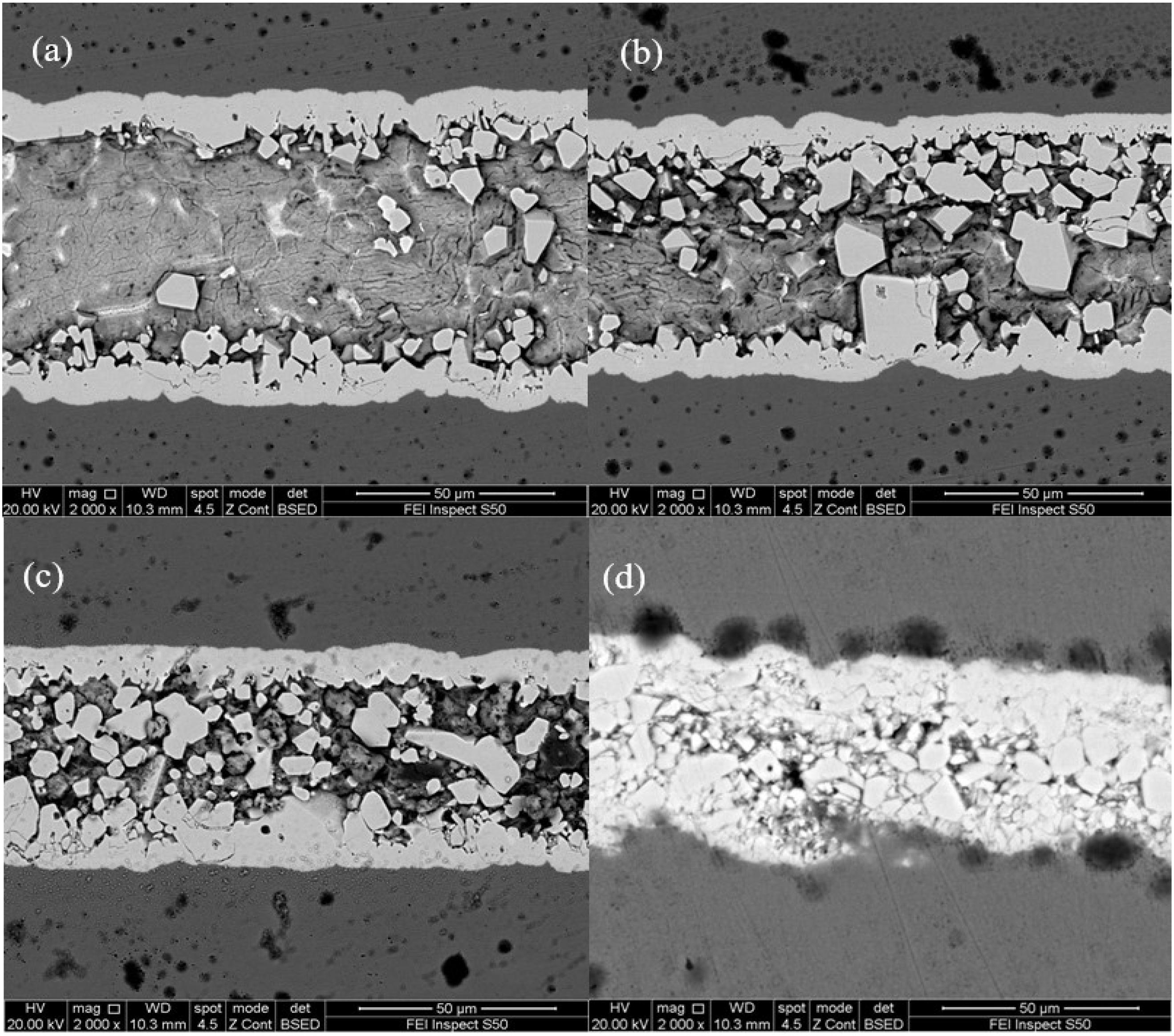
Figure 1. Solder joints with different bonding time: (a) 10 min, (b) 15 min, (c) 40 min, and (d) 180 min.
In order to further study the Ni3Sn4 joints in 3D structure, finite element code was selected to calculate the stress–strain distribution. Three-dimensional finite element model can be established with a SOLID186 element; the solder joint has a diameter of 150 μm and a height of 70 μm; the size of the Cu substrate is 150 μm × 150 μm. For the finite element simulation, Garofalo-Arrhenius creep model (Xiong Ming et al., 2020) can be utilized to describe the creep and stress–strain of the solder joints during thermal cycle loading; the properties of Cu substrate do not change much with the temperature, so it is assumed that the material is a linear elastic material, as shown in our previous work (Xiong Ming et al., 2020; Zhang et al., 2020b). In addition, for the post-processing, the maximum stress–strain in the critical node of solder joints was used to evaluate the stress–strain response. Figure 2a shows the shear stress in the Ni3Sn4 solder joints; the results indicate the shear stress distribution in the three-dimensional 3D structure with different colors, and the maximum shear stress with red color was observed in the middle of Ni3Sn4 IMC. In lead-free soldering, the Cu-Sn IMCs were the stress concentration locations (Ghosh et al., 2017; Li et al., 2018; Zhang et al., 2020a). Therefore, this area along the Ni3Sn4 IMC layer was demonstrated to be the critical location, which may be the failure zone in service. The CTE mismatch among Ni3Sn4, Ni, and chip can induce the phenomenon. Moreover, the Ni3Sn4 is a brittle phase, and combining the stress concentration, the cracks can be produced and propagated in the Ni3Sn4 IMC. Figure 2b displays the cracks along the Ni3Sn4 IMC in the experiment (Liu et al., 2016). Figures 2a,b confirm that the stress concentration area is the area where cracks appear, and the experimental results agree well with the finite element simulation results. Figure 2c plots the shear stress history of the stress concentration location in the solder joints with different IMC thickness; it was found that with the increase in IMC thickness, the shear stress increased obviously under three thermal cyclic loading, and the shear stress induced the IMCs to break away from the interface in service (Teo and Sun, 2008). Figure 2d plots the equivalent creep strain time history of IMCs joints with different IMC thickness. It was demonstrated that an increase in the IMC thickness can dramatically cause an increase of equivalent creep strain; the IMC joints are the key part of the 3D assembly, and the largest creep strain was observed in the IMC joints. Moreover, the fatigue life of solder joints was predicted with the fatigue life prediction model (Nf = (0.0405εacc)−1) based on the largest equivalent creep strain. The fatigue life of solder joints with different IMC thickness was calculated as shown in Figure 2e. It was observed that the IMC thickness can impact the fatigue life of solder joints significantly. An increase in the Ni3Sn4 thickness induced an increase in the fatigue life markedly, and a similar phenomenon was found in both Sn3.9Ag0.6Cu solder joints (Choudhury and Ladani, 2015) and Sn3.8Ag0.7Cu solder joints in 3D packaging (Zhang et al., 2017). From Figure 2e, the solder joints with 90% IMC thickness reduced the fatigue life predicted to about 23% compared to the case with 5% IMC thickness. Moreover, the experimental results agreed well with the calculation results. Therefore, in 3D chip stacking, an increase in the IMC thickness to carry out high-temperature service may decrease the fatigue life, and how to enhance the fatigue life of IMC joints may be an important topic in 3D chip stacking.
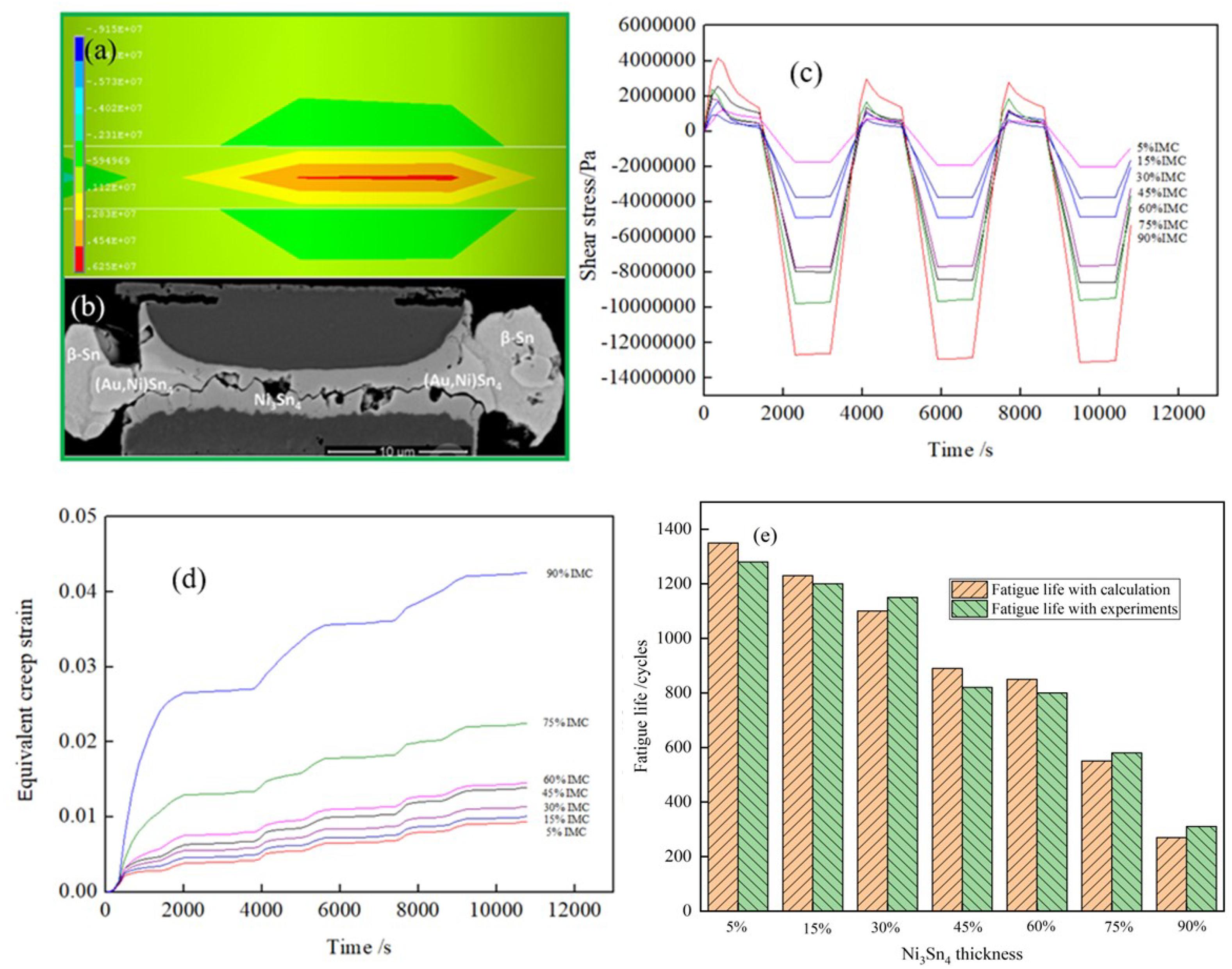
Figure 2. Reliability of solder joints: (a) Shear stress distribution, (b) Failure of solder joints (Liu et al., 2016), (c) Shear stress history of solder joints, (d) Equivalent creep strain, and (e) Fatigue life of solder joints.
Conclusion
The formation of Ni3Sn4 IMC with different bonding time using TLP bonding was studied. An increase in the bonding time can cause an increase in the Ni3Sn4 thickness dramatically. When the bonding time is 180 min, complete Ni3Sn4 was formed. Moreover, the maximum shear stress was observed in the middle of Ni3Sn4 IMC joints in the 3D structure; with the increase in the Ni3Sn4 thickness, the fatigue life of solder joints was reduced markedly.
Data Availability Statement
The original contributions presented in the study are included in the article/supplementary material, further inquiries can be directed to the corresponding author.
Author Contributions
LZ analyzed and interpreted the patient data and was a major contributor in writing the manuscript. S-JZ was responsible for revising the grammar of the manuscript. Both authors read and approved the final manuscript.
Funding
This work was carried out with the support of the State Key Laboratory of Advanced Welding and Joining, Harbin Institute of Technology (AWJ-19Z04), Major State R&D Program of China (2019YFF0217400), and the Central Plains Science and Technology Innovation Leading Talents Program (ZYQR20180030).
Conflict of Interest
LZ and S-JZ were employed by Zhengzhou Research Institute of Mechanical Engineering Co., Ltd.
References
Chen, W. Y., and Duh, J. G. (2017). Suppression of Cu3Sn layer and formation of multi-orientation IMCs during thermal aging in Cu/Sn-3.5Ag/Cu-15Zn transient liquid-phase bonding in novel 3D-IC technologies. Mater. Lett. 186, 279–282. doi: 10.1016/j.matlet.2016.10.006
Choudhury, S. F., and Ladani, L. (2015). Effect of intermetallic compounds on the thermomechanical fatigue life of three-dimensional integrated circuit package microsolder bumps: finite element analysis and study. J. Electron. Packag. 137:041003.
Ghosh, G. (2000). Coarsening kinetics of Ni3Sn4 scallops during interfacial reaction between liquid eutectic solders and Cu/Ni/Pd metallization. J. Appl. Phys. 88, 6887–6896. doi: 10.1063/1.1321791
Ghosh, R., Kanjial, A., and Kumar, P. (2017). Effect of type of thermo-mechanical excursion on growth of interfacial intermetallic compounds in Cu/Sn-Ag-Cu solder joints. Microelectron. Reliab. 74, 44–51. doi: 10.1016/j.microrel.2017.05.011
Li, W. Y., Zhang, X. P., Qin, H. B., and Mai, Y. W. (2018). Joule heating dominated fracture behavior change in micro-scale Cu/Sn-3.0Ag-0.5Cu/Cu(Ni) joints under electro-thermal couples loads. Microelectron. Reliab. 82, 224–227. doi: 10.1016/j.microrel.2017.10.031
Liu, Y. X., Chen, Y. T., Gu, S., Kim, D. W., and Tu, K. N. (2016). Fracture reliability concern of (Au, Ni)Sn4 phase in 3D integrated circuit microbumps using Ni/Au surface finishing. Scr. Mater. 119, 9–12. doi: 10.1016/j.scriptamat.2016.02.025
Panchenko, I., Bickel, S., Meyer, J., Mueller, M., and Wolf, J. M. (2018). Characterization of low temperature Cu/In bonding for fine-pitch interconnects in three-dimensional integration. Jap. J. Appl. Phys. 57:02BC05. doi: 10.7567/jjap.57.02bc05
Teo, J. W. R., and Sun, Y. F. (2008). Spalling behavior of interfacial intermetallic compounds in Pb-free solder joints subjected to temperature cycling loading. Acta Mater. 56, 242–249. doi: 10.1016/j.actamat.2007.09.026
Xiong, M. Y., and Zhang, L. (2019). Interface reaction and intermetallic compound growth behavior of Sn-Ag-Cu lead-free solder joints on different substrates in electronic packaging. J. Mater. Sci. 54, 1741–1768. doi: 10.1007/s10853-018-2907-y
Xiong Ming, Y., Zhang, L., He, P., and Long, W. M. (2020). Stress analysis and structural optimization of 3D IC package based on the Taguchi method. Soldering Surface Mount Technol. 32, 42–47. doi: 10.1108/ssmt-04-2019-0016
Zhang, L., and Gao, L. L. (2015). Interfacial compounds growth of SnAgCu (nano La2O3)/Cu solder joints based on experiments and FEM. J. Alloys Compd. 635, 55–60. doi: 10.1016/j.jallcom.2015.02.110
Zhang, L., Jiang, N., He, P., and Zhong, S. J. (2020a). Properties and microstructure evolution of Sn-Cu-Ni/Cu joints bearing carbon nanotubes and grapheme nanosheets for solar cell. J. Mater. Sci. 31, 21758–21766. doi: 10.1007/s10854-020-04688-7
Zhang, L., Long, W. M., He, P., Guo, Y. H., Sun, L., and Jiang, N. (2020b). Effect of Ti nanoparticles on the microstructures and properties of Sn interconnect materials for 3D packaging. Rare Met. Mater. Eng. 49, 4336–4340.
Zhang, L., and Liu, Z. Q. (2020). Inhibition of intermetallic compounds growth at Sn-58Bi/Cu interface bearing CuZnAl memory particles (2-6μm). J. Mater. Sci. 31, 2466–2480. doi: 10.1007/s10854-019-02784-x
Zhang, L., Liu, Z. Q., Chen, S. W., Wang, Y. D., Long, W. M., Guo, Y. H., et al. (2018). Materials, processing and reliability of low temperature bonding in 3D chip stacking. J. Alloys Compd. 750, 980–995. doi: 10.1016/j.jallcom.2018.04.040
Keywords: 3D IC, TLP bonding, IMC thickness, fatigue life, solder joints
Citation: Zhang L and Zhong S-J (2021) Effect of Ni3Sn4 on the Thermo-Mechanical Fatigue Life of Solder Joints in 3D IC. Front. Mater. 8:645782. doi: 10.3389/fmats.2021.645782
Received: 24 December 2020; Accepted: 15 April 2021;
Published: 13 May 2021.
Edited by:
Marco Salerno, Italian Institute of Technology (IIT), ItalyReviewed by:
Wojciech Jerzy Stêpniowski, Military University of Technology in Warsaw, PolandSudagar J, VIT-AP University, India
Abhijit Dasgupta, University of Maryland, College Park, United States
Copyright © 2021 Zhang and Zhong. This is an open-access article distributed under the terms of the Creative Commons Attribution License (CC BY). The use, distribution or reproduction in other forums is permitted, provided the original author(s) and the copyright owner(s) are credited and that the original publication in this journal is cited, in accordance with accepted academic practice. No use, distribution or reproduction is permitted which does not comply with these terms.
*Correspondence: Liang Zhang, emhhbmdsaWFuZ0Bqc251LmVkdS5jbg==