 Manwen Liu
 Zheng Li
 Zhi Deng4
- 1Institute of Microelectronics, Chinese Academy of Sciences, Beijing, China
- 2School of Physics and Optoelectronic Engineering, Ludong University, Yantai, China
- 3Hunan Zhengxin Micro Detectors Limited, Beijing, China
- 4Department of Engineering Physics, Tsinghua University, Beijing, China
- 5Nuctech Company Limited, of Detector ASIC Laboratory, Beijing, China
An X-ray pulsar is a remnant of massive star evolution, collapse, and supernova explosions. It has an extremely stable spin cycle and is known as the most accurate astronomical clock in the natural world. It presents high-precision navigational information, such as the location, speed, time, and attitude, which are used in deep space exploration and interstellar flight, such as the X-ray pulsar navigation (XPNAV). However, the energy of the X-ray from the pulsar is very low and its signal is very weak; this X-ray is known as the soft X-ray. In the low and medium energy radiation spectroscopy, the semiconductor detectors, especially the silicon drift detectors (SDD), achieve the best energy resolution. In this study, a 314 mm2 and a 600 mm2 double-sided spiral hexagonal silicon drift detector (DSSH-SDD) single cell for the pulsar soft X-ray detection is analyzed based on ultra-pure high-resistance silicon. The DSSH-SDD device is fabricated using ultra-pure high-resistivity silicon substrates patterned with ion-implanted electrodes. This study proposes a model capable of reaching a large area of 314 mm2 or 600 mm2 single cell and maintaining an optimal drift electric field. The design, modeling, 3D simulation, and the fabrication of the model are performed to analyze the physical performance of the DSSH-SDD. The electrical characteristics of the as-processed SDD chips, including leakage current, anode capacitance, and the spiral resistor current under the positive and negative biases are measured, and the energy resolution test is performed at the Tsinghua University. The energy resolution is an important indicator of the detector and is often expressed by full width at half maximum (FWHM). The results obtained in this study can be applied in the future for novel, flexible, large-area, high-resolution ionizing radiation detection systems capable of providing quantitative and real-time information of the relative position of spacecraft and pulsars through the pulsar X-ray radiation.
Introduction
Pulsars are rotating neutron stars formed owing to the collapse and the supernova explosion created when the life of a massive star ends (Burrows, 2000). The mass of neutron stars is larger than that of the Sun, and they are only approximately 25 km in diameter; they are primarily composed of neutron-rich matter near and above nuclear densities. The pulsars rotate at extremely high speeds, with the observed spin periods ranging from 1.4 ms to more than 1 s (Hessels et al., 2006). These rotation periods are very stable and can achieve the precision of atomic clocks. An array of these distant high-precision clocks is currently being used in a global effort to detect the gravitational waves from super-massive black holes at cosmic distances (Ho et al., 2015).
The X-ray pulsar navigation involves the use of an X-ray detector installed in the spacecraft, which detects the pulsar radiation of X-ray photons, measures the pulse arrival time, and extracts the pulsar image information. The autonomous high-precision orbit of the spacecraft is determined using the corresponding signal and data processing, and the navigation parameters such as the time and posture are realized. X-ray pulsars provide independent external space–time benchmarks for navigation through constellations, without the overall rotation problem of the constellation. It primarily requires autonomous navigation and operational control for an extended period of time. Furthermore, the X-ray pulsar navigation technology (XPNAV) is fully applicable in deep space exploration and interstellar flight missions, as well as surface cruisers for planets without a dense atmosphere. Therefore, the X-ray pulsar navigation is a new and effective method to realize high-precision and seamless autonomous navigation of spacecraft (Witze, 2018).
The energy of the pulsar (such as the Crab system) X-ray, known as the soft X-ray, is very low, mostly ranging from 0.1–10 keV (Rho et al, 2003); these X-rays are very difficult to detect (Chauvin et al., 2017). However, the pulsar X-rays can be widely applied in various fields. For example, X-ray pulsar provides a new idea and realization way for autonomous navigation of navigation satellites (Shuai and Li, 2017). For deep space exploration and interplanetary missions, X-ray pulsar navigation has its advantages over the GPS system and ground-based deep space network (Mitchell and Keith, 2017). It promotes the development of modern astronomy, space physics, astrometry, and other disciplines and is conducive to the integration of disciplines and interdisciplinary research (Liu et al, 2015). Their detection can help in understanding the beginning and the development of the stars, as well as the rules of outer space. Additionally, the detection of the thermal radiation of a neutron star is extremely important in the analysis of the neutron star matter, the neutron star structure, and the polar magnetospheres (Helfand et al., 1980).
Extensive research has been conducted in the detection of X-rays and other sources of pulsars (Fritz et al., 1969; Kulkarni et al., 1992; Archibald et al., 2009; Hermsen et al., 2013). For example, the X-ray flares from the post-merger millisecond pulsars (Dai et al., 2006), the features in the X-ray spectrum of an ordinary radio pulsar (Kargaltsev et al., 2012), and the ultraluminous X-ray sources have been analyzed to determine the presence of neutron stars (Israel et al., 2017). This study proposes the development of a physical model for the nonthermal emission of pulsars. The spectra of the X-ray pulsars are fit across seven orders of magnitude in energy with only four physical parameters (Torres, 2018).
Several studies have been conducted on the detection of X-rays, such as X-ray photo detectors (Büchele et al., 2015) and the detection of X-ray photons by using solution-processed detectors (Yakunin et al., 2015). However, the X-rays obtained from the pulsars are mainly soft X-rays, and it is challenging to separate the pulsar X-rays from other background X-rays, which requires a detector capable of good efficiency and high energy resolution. Silicon detectors are widely used in X-ray and high-energy particle detection owing to their numerous advantages, such as high energy resolution, the advanced fabrication and processing technology, and the integrated electronic readout circuit technology (Kern et al., 2013). They have been used to detect the existence of particles, such as the Higgs boson particle at the Large Hadron Collider (Stapnes, 2007; Della Negra et al., 2012). The collection efficiency is responded to the transient current and the transient/response time of the electrons and holes. As we studied before, though the transient/response time of the SDD is less than 1 ns(Zhang et al., 2020), the charge collection can be in the level of 103–104 e due to that the transient current is in the level of a few amperes (Ding et al., 2015). In the application of ALICE and NA45-CERES of CERN’s LHC and LEP (Guazzoni, 2013), the silicon drift detector and its array have been worked for a few years, which verified the stability of the detector. In addition, the SDD system is usually accompanied by a temperature-controlled package to enhance its temperature stability. The silicon drift detector (SDD) is a special type of silicon detector, which is capable of low capacitance and high-energy resolution (Rehak et al., 1989; Rehak et al., 2010; Li, 2013; Li and Chen, 2016). However, the detectors are generally focused on a small area unit cell (Zampa et al., 2009). This study focuses on a large area double-sided spiral hexagonal silicon drift detector (DSSH-SDD) fabricated with ultra-pure high-resistance silicon for the pulsar soft X-ray detection. The spiral cathode electrode is set as an automatic voltage distribution mechanism. As the spiral p+ cathode is formed by ion implantation, it is a continuous resistance chain, and the resistance distribution is related to the spiral gap, width, and ion implanted concentration according to the calculations and the proposed design.
The effective parallel noise ENCpar and the effective serial noise ENCseries can be calculated by using the following equations:
where Ileak is the leakage current of the detector, Ct is the input capacitance of the detector, and tpeak is the peak response time of the output signal (Rehak et al., 1989). From Eq. 1, ENCseries is observed to be proportional to the square of the input capacitance. Therefore, it is important to decrease the input capacitance while limiting the noise in the detector and improving the energy resolution. Additionally, the silicon drift detector is superior when compared to the traditional detector due to its extremely small input capacitance, which is independent of the effective sensitive area of the detector.
The SDD is currently applied in high-resolution, high-count rate pulsar X-ray spectroscopy analysis and is determined to be one of the best detectors for pulsar X-ray detection. The modern SDDs are based on a unique design that enables them to achieve much higher performance than the lithium drift detectors or the other types of silicon detectors. Specifically, they are far less susceptible to electronic noise, which can be especially observed for larger detector areas and low X-ray energies.
However, the intensity or light flux of the pulsar X-rays is extremely low, requiring one or two square meters of SDD to detect the signals as navigation information in outer space. The resolution-based formation method of silicon drift detectors presented in previous studies is unsuitable for the formation of a detector array in the size of the square meter level required for XPNAV owing to their small single cell size (<100 mm2), high cost, and extremely large dead area. The size of a single SDD cell must therefore be significantly increased. In this study, a double-sided spiral hexagonal SDD is fabricated with a single cell size over 3 cm2, which will be increased to a square meter size array in the future for the XPNAV. Specifically, the spiral SDD does not require a voltage divider because it can be used as an automatic voltage distribution mechanism, which avoids many design and process complexities.
In Su et al. (2020), the author has summarized various parameters of the silicon material and other materials of X-ray direct detectors. In this work, some parameters of SDD and perovskites X-ray direct detectors have been listed in Table 1.
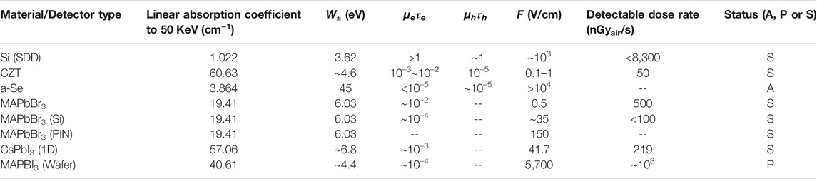
TABLE 1. Performances and parameters of Si and a perovskite X-ray direct detector. W± is the generation of carriers (EHP) creation energy. The central parameter is the product of carrier mobility and mean carrier lifetime (μτ), which is normally called the range of the carrier. The F parameter is the largest electric field. In the “status” column, A is amorphous, S is single-crystal, and P is polycrystalline.
Design, Modeling, and Simulation of the 314 mm2 Hexagonal Double-Sided Spiral Silicon Drift Detector
An ultra-pure high-resistance silicon substrate (≥6,000 Ω-cm, lifetime ≥1 ms, and n-type doping of 1 × 1012 cm3 phosphorus) is used in the proposed design of a 314 mm2 double-sided spiral hexagonal silicon drift detector for the pulsar soft X-ray detection. As shown in Figure 1 (in this figure, we have simplified the graph of the device so that it can be seen more clearly), the device has two kinds of electrodes: anode (n+) and cathode (p+). The anode electrode is a small area, which is subjected to n-type doping of 1×10¹⁹/cm3 phosphorus. The side including the anode electrode is defined as the front side and the collecting plane, and the other side is defined as the back side and the incident plane. The front and the back sides are covered in a spiral shape by the cathode electrodes (p-type doping of 1×10¹⁹/cm3 boron) cover. The designed SDD cell is therefore called the double-sided spiral hexagonal silicon drift detector (DSSH-SDD) cell. The spiral cathode rings are the drift rings. When the bias voltages are applied on the anode electrode and on the different rings of the cathode electrode, a drift channel is formed in the inner depleted region of the SDD to transport the electrons, which are generated by the illumination of the X-rays, to the back side of the SDD, that is, to the anode electrode, forming a current signal. This signal is amplified and treated by a readout electronic chip, such as an ASIC, to produce an SDD charge signal. This section explains the design and the modeling of a spiral SDD.
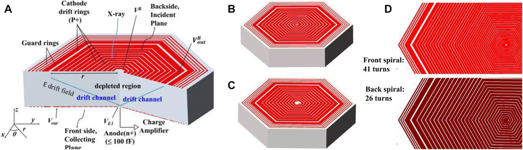
FIGURE 1. Schematic of the 314 mm2 DSSH-SDD. (A) The figure with all the parameters; (B) the front side and (C) the back side of the hexagonal double-sided spiral SDD; and (D) cut planes of the structure.
To ensure the shortest drift time and drift channel, the drift channel must be maintained as a straight line in the body of the detector substrate. There is no θ dependence on the negative electric potential, owing to the cylindrical symmetry, which is given by the following:
In an SDD, the width of the cathode electrode ring is denoted by W(r), and the distance from the anode electrode center to the cathode rings, that is, the radius, is denoted by r. For a large-area SDD, the size in the r direction is much larger than that in the z direction, which results in the following approximation for the negative electric potential:
where z is the axis along the detector thickness, r is the coordinate along the radius of the detector, and θ is the angular coordinate. Φ(r) and Ψ(r) are the surface potentials of the front (z = 0) and the back (z = d, where d is the detector thickness) side, respectively, which are given by the following:
where Φ(r) and Ψ(r) are the boundary conditions of the SDD, whose forms are determined by the calculus of the variation method to produce the best drift electrical field in the SDD (Li and Chen, 2016). In the design of the 314 mm2 hexagonal double-sided spiral silicon drift detector for the XPNAV, potential distribution of the back side is considered to be proportional to that of the front side as follows:
Furthermore, the results of the calculus of variation produce the best electric field along the drift path as a constant drift electric field, Edr,r.
In this study, the following relationship between the SDD cathode spiral ring width W(r) and pitch p(r) on the front surface is considered as follows:
where β is a proportionality constant. To generate the design of a spiral SDD, as shown in Figure 1A, the relationship between p(r) and radius, r, is determined through calculation as follows:
where p1 is the pitch of the first ring and r1 is the radius of the first ring. Here,
The first spiral pitch can be determined by the SDD geometry and by the boundary conditions as follows:
where ρs is the square resistance of the spiral-shaped cathode ion-implanted layer, I is the total current of the spiral-shaped cathode, and α is a parameter dependent on the geometric shape of the spiral cathode, which gives a ring circumference, α·r. The hexagonal shape of the spiral SDD is the most suitable because it is the shape closest to a circle but can form a compact SDD array. For a regular hexagon, α = 6. R in Eq. 9 is the radius of the SDD (radius of the last ring), and r1 is the radius of the first ring. Furthermore, VE1 and Vout are the absolute values of the bias voltages on the first and the last rings of the spirals of the SDD (front side), respectively.
The front surface potential of the spiral SDD can be determined by the following equation:
The electric field along the front surface of the detector is as follows:
The average drift electric field inside the detector is as follows:
where Vfd = qNDd2/2ε0ε is the fully depleted voltage of the SDD. In this instance, the spiral cathode on the front surface of the SDD can be determined as follows:
Here, θ is the angle of the continuous increase in the spiral rotation. The 3D schematic of the 314 mm2 DSSH-SDD can be obtained through calculation and parameter design, as shown in Figure 2 (in this figure, the design details are clearly shown, including the size of the hexagonal cell and the electrodes). The hexagonal design is advantageous as it fits the array and presents an excellent electric field distribution in the unit cell.
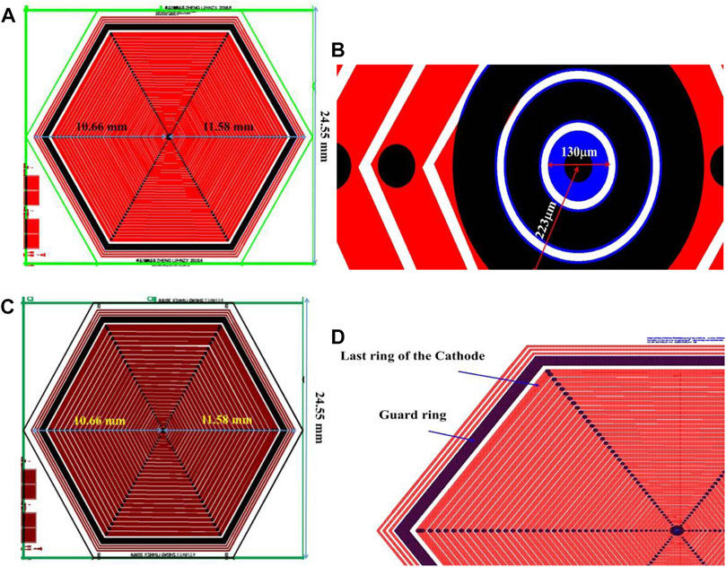
FIGURE 2. Design details of the 314 mm2 DSSH-SDD. (A) The detail and the sizes of the front side; (B) the detail and the sizes of the back side; (C) the sizes of the front anode electrode and the front first cathode electrode; and (D) the last ring of the front cathode and the cathode guard rings.
The current of the spiral cathode is determined by the largest bias voltage and resistance of the spiral cathode. The drift electric field is generally between 100 and 500 V/cm. The total resistance of the spiral cathode depends on its total length, width, ion concentration dose, and depth. For a spiral cathode current of 50 mA, the total power consumed by the spiral is less than 25 mW and the total power consumption is reduced for a smaller current. However, the function of the spiral cathode as a voltage divider is diminished. Therefore, the power consumption and the voltage divider function of the spiral cathode must be balanced to achieve an optimum design. Consequently, an SDD with a radius of R = 1 cm is designed in this study, as shown in Figure 2. The current of the spiral cathode is 20 mA, Vout = 250 V, and VB = Vfd = 72 V.
The spiral pattern of the back side can be matched with that of the front side with the definition of the backside surface potential, as given in Eq. 5. The front side cathode electrode has 41 rings and the backside spiral cathode electrode has 26 rings. The electric potential and electric field profiles of the SDD are plotted, as shown in Figure 3. The simulations are carried out by Silvaco and Sentaurus TACD software. From Figures 3A,B, it can be observed that the potentials of the back and the front sides are not constant and exhibit gradient variations. Additionally, the electric field along the drift channel is observed to be nearly constant, and the value is approximately 180 V/cm. In practical applications, only an approximate electric field value in the drift channel is sufficient, which is close to a constant value. The electron drift time in the drift channel is determined to be proportional to the radius of the SDD through calculations, and the maximum drift time is in the order of microns.
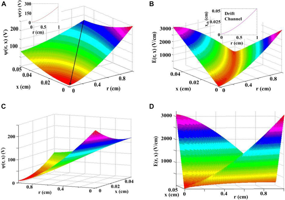
FIGURE 3. 3D simulations of electric potential distribution and electric field distribution of DSSH-SDD. (A) and (C) are the 3D electric potentials of the silicon drift detector at different viewing angles; (B) and (D) are the 3D electric field distributions of the SDD, and the drift channel is within the SDD body, pointing towards the anode electrode.
As shown in Figure 3A,B the smallest bias voltage is set near the front side anode electrode, and the largest bias voltage is set in the outer ring of the front side spiral cathode electrode. This results in the formation of a “potential net” due to the potential gradient. The electrons are accumulated by the anode after they are transported through the potential net to the lowest potential point. The 3D distribution of the total electric field can be obtained by differentiating the electric potential. The calculation and the presentation of the 3D electric field profile in an SDD is the novelty of this study. As shown in Figures 3B,D, the drift channels are more clearly visible in the mapping of the electric field distributions, and they directly point to the collecting anode. A uniform electric field (close to a constant, as indicated by the same color in the mapping) is clearly observed in the drift channel, which is obtained because of the proposed design. However, the incorrect application of bias voltages results can have adverse consequences. When the voltage applied to the last ring of the front cathode electrode is too high, the drift channel is extended out of the SDD. When the voltage applied to the first ring of the backside cathode is too high, the drift channel does not point to the front anode. If the voltages applied to the last ring of the front cathode and to the first ring of the backside cathode are both too high, it results in a drift channel outside the SDD body and does not point towards the collection anode. In these cases, either the SDD leakage current is high (reach-through effect) or the signal is not collected by the collection anode, or both.
Fabrication of the Hexagonal Double-Sided Spiral Silicon Drift Detector
Figure 4A shows the top view of the front-side design of a 314 mm2 DSSH-SDD. The collection electrode, or the anode, has a very small area, providing minimal input capacitance, which ensures a minimal amount of noise and, therefore, high energy resolution. The detector has a radius of 1 cm, the effective sensitive area is 314 mm2, and the radius of the first ring is 200 mm. The hexagonal SDD can then be designed with a 41 turn spiral on the front side and a 26 turn spiral on the backside. The bias voltage is 10 V in the first ring and 250 V in the last ring of the front side spiral. The average electric field in the drift channel is 173 V/cm.
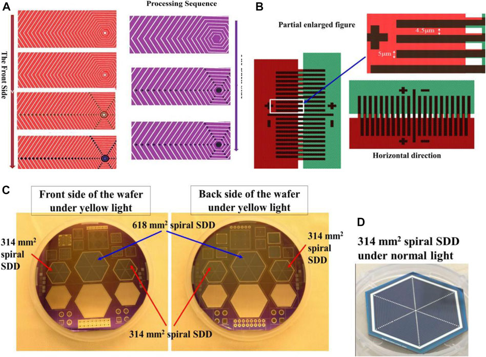
FIGURE 4. (A) shows the front-side design top-view figure of the 314 and 600 mm2 DSSH-SDD; (B) shows the partially enlarged detail of the mask alignment marks; and (C) is the wafer of the silicon drift detectors. This wafer includes the detector introduced in this article, as well as the 618 mm2 spiral SDD, small-area spiral SDDs, spiral SDD array, and circular hexagonal SDDs; (D) is the 314 mm2 spiral SDD under normal light.
Figure 4B shows the partially enlarged details of the mask alignment marks. Considering the vertical direction as an example, the left scale spacing is 4.5 mm, and the right scale spacing is 5 mm. If there are no errors in the operation, the long scale mark (in the center) on the left coincides exactly with that on the right. Any errors during the operation can be estimated by the deviation of the corresponding scale. Practically, the maximum error made by a human operator is approximately half of the misalignment produced by the first short scale mark (0.25 mm), which is the accuracy of the mask alignment.
The fabrication process is unique and complex owing to the novelty of the proposed large-area DSSH-SDD, which requires a novel processing procedure. This includes special defeat gettering oxidation, special double-sided photo lithography and etching, double-sided ion implantations with specific protection considerations, metallization, annealing, and surface passivation. Each step requires rigorous inspections and has strict requirements for uniformity to maintain the minimum number of defects in each process. All these procedures ensure excellent electrical properties of the SDD unit. The SDD fabrication has been performed in our Class-100 cleanroom at the Hunan Zhengxin Micro Detector Limited Company at a constant temperature (24°C) and constant humidity (40%). Figure 4C shows the photographic images of the as-processed Si wafer (front side and backside) with SDDs. Figure 4D shows the 314 mm2 DSSH-SDD unit cell, and the Al point on the front side can be clearly observed. The SDD will respond to visible light. So it is usually using a thin Al layer or other metal layer to block visible light. The radiation will increase the noise floor, and large enough radiation will affect the resolution of the signal due to large leakage current.
Figure 5 shows a simplified process flow chart in which different colors represent different materials. The actual processing is too complicated to be illustrated here. In Figure 5, the oxidation process has been omitted. As observed in Figure 5A, the double-side photolithography marks can be formed, which can determine the exact position of the photolithography and the following process. The alignment accuracy is less than 0.25 microns owing to our technological innovation. Subsequently, the photolithography can be formed on each side for ion implantation based on the double-sided marks. Figure 5B shows the front side cathode P+ photo lithography and ion implantation. After the front-side photolithography and etching are performed, the back side is covered by a layer of photoresist before the ion implantation process to protect it from ions and other impurities. Figure 5C shows the backside cathode P+ photolithography and ion implantation. In this process, the area of the anode does not need to be retained. Figure 5D shows the front side cathode N+ photo lithography and ion implantation with the protection of the back side. Figure 5E shows the process of annealing and deoxidation. Figure 5F shows the metallization and surface passivation. A microscopic examination must be conducted after every etching step. When all the processes are completed, the chip must be sealed and stored in an environment with constant temperature and humidity. The guard rings are not shown in Figure 5.
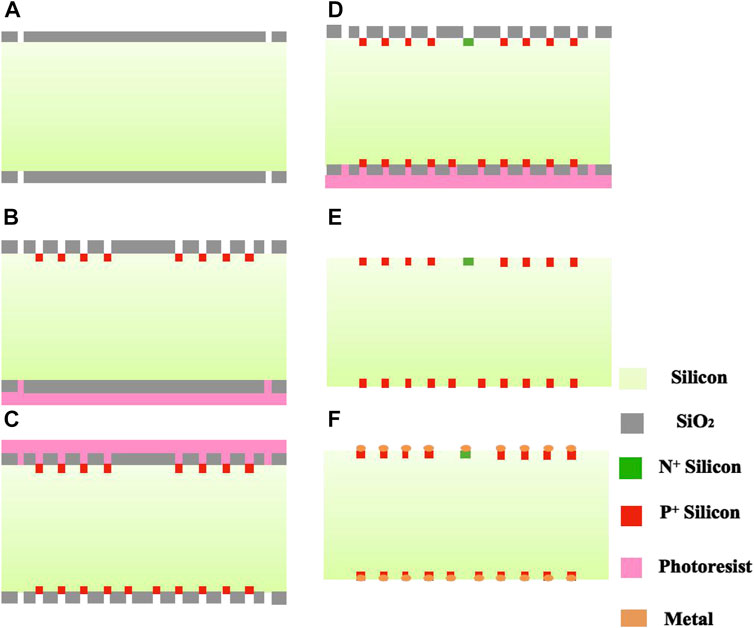
FIGURE 5. Simplified process flow chart. (A) Formation of the double-sided photo lithography marks; (B) the front side photo lithography and P+ ion implantation with protection of the back side; (C) the back side photo lithography and P+ ion implantation; (D) the front side photo lithography and N+ ion implantation with protection of the back side; (E) annealing and deoxidation; and (F) metallization and surface passivation.
Current–Voltage (I–V) and Capacitance–Voltage (C–V) Characteristics in Room Temperature With Probe Station
The electrical characteristics of the as-processed SDD chips, including leakage current, anode capacitance, and the spiral resistor current under the positive and negative biases, are measured. The measurement equipment used in this study includes a Keysight Technologies B1505a semiconductor device analyzer, Carl Zeiss Microscopy GmbH, and an orthopedic material microscope Axio Lab. The chip is placed at a CL-6 probe station. Figure 6A shows the leakage current and the bias voltage (I–V) characteristics of a 314 mm2 SDD at room temperature. It can be observed from Figure 6A that the leakage current of the 314 mm2 hexagonal double-sided spiral SDD at room temperature is less than 5 nA. This indicates that at the working temperature (assumed as −50°C to −25°C), the leakage current will be low enough to ensure adequate performance. Figure 6B shows the capacitance and the bias voltage (C–V) characteristics. The capacitance is only relevant to the anode electrode area and is fixed when the SDD anode structure is designed. In the proposed design, it should be less than 100 fF according to the designed area of the anode, as shown in the simulation results (dotted line in Figure 6B). Since the system noise in the C–V setup used in the study is 600 fF, the capacitance lower than this value could not be measured. Figure 6C–E show the spiral resistor current under the positive and negative biases for the 314 mm2 hexagonal double-sided spiral SDD at room temperature with the bias voltages of 10, 50, and 100 V. It is nearly linear, and the value is approximately 4 mA at 50 V, which is equal to the design value.
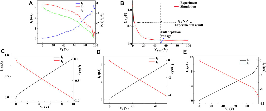
FIGURE 6. Test results of the 314 mm2 DSSH-SDD. (A) Leakage current and bias voltage (I–V) characteristics; (B) capacitance and bias voltage (C–V) characteristics; and (C), (D), and (E) the spiral resistor current under positive and negative biases at room temperature with bias voltages of 10 V, 50 V, and 100 V.
Energy Resolution Measurement at Low Temperature With Pre-amplification Electric Circuit
The energy resolution test was performed at the Tsinghua University. The hardware includes low noise linear power supply: power supply unit of front amplifier circuit, Guwei 60,300 dc power supply, load regulation rate <10 mV, ripple and noise <2 mVrms, voltage accuracy 5 ± 0.25 V; oscilloscope: fluorescence oscilloscope Tektronix DPO4034B, four channels, bandwidth 350 MHz, sampling rate 2.5 gs/s; and high voltage, main amplifier plug-in and NIM case: Canberra 3106D, ±6000 V bias range, 300 uA power supply current, noise and ripple peak <3 mV; Canberra 2026 is used for the main amplifier module. The forming time is adjustable from 0.5–to 12 us, and Gaussian and trapezoidal forming are available, with stacking correction and live time correction. The NIM case is a Wiener UEP 15,5 slot, power 150 W, ±6 V, ±12 V, ± 24 V power supply; multi-channel, energy spectrum acquisition instrument: ortec-easy MCA, 8 K channel, high-speed conversion time (<2 us) provides a dead time correction logic input port. The test software used was MAESTRO. MAESTRO is ORTEC’s basic spectrum acquisition software that recognizes and processes all forms and models of the MCA signals of ORTE. The dose of the X-ray used for the radiation test is very small, in the order of 10 grads. As for SDD, it is radiation soft and cannot take more than 100 grads.
This test mainly involves measuring the leakage current and the energy resolution of the 314 mm2 spiral SDD integrated readout electronics at low temperatures. The energy resolution, which represents the detector’s ability to distinguish similar energy peaks, is an important indicator of the detector and is often expressed by full width at half maximum (FWHM). The resolution of the detector corresponds to the energy required to produce an electron–hole pair, the energy of the incident particle, etc. It is also affected by the leakage current, junction capacitance, temperature, electronic noise, bias voltage, and other factors of the detector material. Under an appropriate bias voltage, the silicon body area of the detector is completely depleted, and a uniform electric field is generated, resulting in the formation of the drift channel. The carrier moves to the collection anode through the drift electric field, is collected, and then amplified and read out by the preamplifier circuit.
The SDD chip test procedures are as follows: 1) Integration and assembly of the SDD and the electronics. The wires connected the anode to the preamplifier circuit. It was necessary to wire the anode of the SDD directly to the input end of the readout electronics to reduce the parasitic parameters and improve the energy resolution. The entire circuit board was welded and electrically tested after the wiring process. When the test was normal, the circuit board, integrated with the SDD detector and the pre-release electronics, was assembled in the vacuum chamber. The setup was then vacuumed and placed in liquid nitrogen. 2) Leakage-current test. The leakage current test was initiated when the internal temperature of the vacuum device in a low-temperature environment had been stabilized. The test instruments used included a high-voltage device and an oscilloscope. The reset time was inversely proportional to the leakage current of the detector because the preamplifier electronics used the reset mode of pulse feedback. The feedback capacitance was known, and the leakage current of the SDD detector could be obtained by measuring the reset time. Therefore, the measurement step involved first using the high-voltage module on the NIM chassis to set the bias voltage. When the bias voltage reached the working voltage, the reset time of the reset sawtooth signal was observed and measured using an oscilloscope. 3) Energy-resolution test. The energy resolution was determined after measuring the leakage current of the detector within the normal range. The radioactive source used in the tests was Fe55. The SDD bias voltage was first applied to the normal working voltage through the high-voltage plug-in on the NIM chassis, the output signal of the front amplifier was connected to the main amplifier plug-in, and the gain and forming time of the main amplifier were adjusted. The signal was then sent to multiple channels for energy spectrum acquisition after the main amplifier forming.
Figures 7–9 illustrate the details of the energy resolution measurement process, which has been explained above. Figure 7 shows the preamplifier electronics. Figure 8A shows the noise component test results, and Figure 8B shows the noise capacitance slope of the preamplifier electronics. The test results demonstrate that the preamplifier performance meets the detector test index. Figure 9 shows the test result of the SDD leakage current in the oscilloscope. The high-voltage module is used to bias the SDD to the working voltage; the reset time is greater than 1 s, and the feedback capacitance is 200 fF, which results in the detector leakage current less than 10 pA. Figure 10 shows the energy spectrum of the Fe55 radioactive sources measured under different bias pressures. The oscilloscope channel signal is shown in Figure 10A. The main amplifier gain is set to 500 times. Figure 10B shows the energy spectrum measured after the bias voltage is adjusted to −300 V, and the FWHM at 5.9 keV is 150 eV.
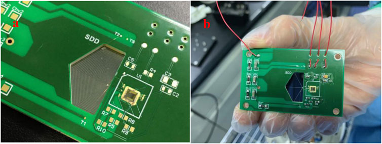
FIGURE 7. (A) DSSH-SDD and electronics integrated assembly and (B) schematic diagram of the preamplifier circuit after wiring.
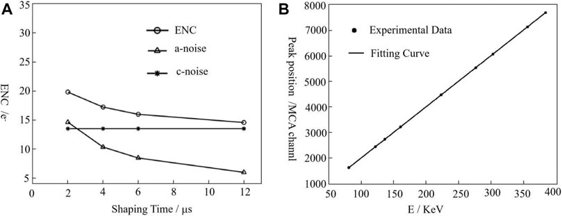
FIGURE 8. Noise analysis of the preamplifier circuit.
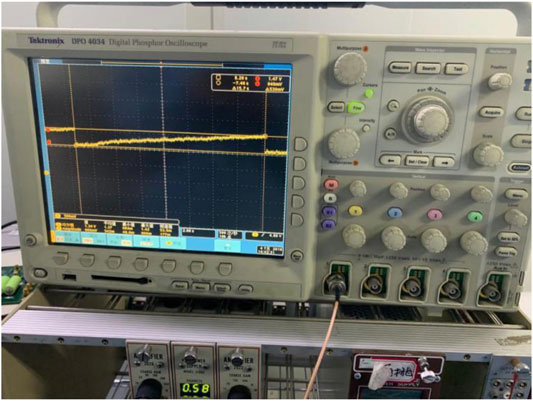
FIGURE 9. Noise capacitance slope of a preamplifier circuit.
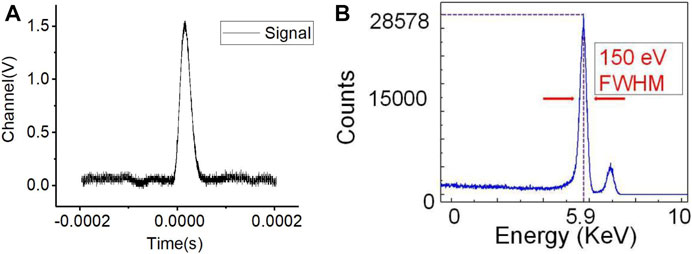
FIGURE 10. (A) an oscilloscope channel signal; (B) SDD energy spectrum with a high voltage of 300 V (absolute value), and the FWHM is 150 eV.
Conclusion
This study presents the application of a novel large-area SDD in the detection of direct soft X-rays. The SDDs designed and fabricated in this study were hexagonal, double-sided, spiral SDDs, with an area of at least 314 mm2. The Current–Voltage (I–V) and Capacitance–Voltage (C–V) characteristics in room temperature with probe station have been presented. The leakage current of the 314 mm2 hexagonal double-sided spiral SDD at room temperature is less than 5 nA. The leakage current and the energy resolution characteristics of the as-fabricated SDD chips were measured at low temperatures. An FWHM of 150 eV was obtained for a 5.9 keV X-ray, which ensures good working performance of the DSSH-SDD. These results can be applied in the future for novel flexible, large-area, high-resolution ionizing radiation detection systems capable of providing quantitative and real-time information of the relative position of spacecraft and pulsars through the pulsar X-ray radiation.
Data Availability Statement
The original contributions presented in the study are included in the article/Supplementary Material, and further inquiries can be directed to the corresponding author.
Author Contributions
ML and ZL conceived the design and optimization of the SDD device structures. ML, ZL, and BX carried out the simulation of the detector. ML, ZL, BX, YL, MF, and LT performed the experiment, analyzed the fabrication processing, and fabricated the devices. ML, MC, ZD, and LH carried out tests and electrical measurements. ML and ZL contributed to the interpretation of the results and writing of the manuscript.
Funding
This work was partly supported by financial support from the Key Project of National Natural Science Foundation of China (Grant No. 11835008), the Youth Science Foundation program of the National Natural Science Foundation of China (Grant No. 12005089), the Yantai Institute for the exchange of driving forces (Grant No. 2019XJDN002), and the Yantai Science and Technology Innovation Development Plan (School-local Cooperation) (Grant No. 2020YT06000324).
Conflict of Interest
Author ZL He was employed by the Nuctech Company Limited of detector ASIC laboratory. Authors BX, YL, MF, LT, and MC were employed by the company Hunan Zhengxin Micro Detectors, Limited.
The remaining author declares that the research was conducted in the absence of any commercial or financial relationships that could be construed as a potential conflict of interest.
Publisher’s Note
All claims expressed in this article are solely those of the authors and do not necessarily represent those of their affiliated organizations, or those of the publisher, the editors and the reviewers. Any product that may be evaluated in this article, or claim that may be made by its manufacturer, is not guaranteed or endorsed by the publisher.
References
Archibald, A. M., Stairs, I. H., Ingrid, S. M., Kaspi, V. M., Scott, V. I., Lorimer, D. R., et al. (2009). A Radio Pulsar/X-ray Binary Link. Science 324, 1411–1414. doi:10.1126/science.1172740
Büchele, P., Richter, M., Tedde, S. F., Matt, G. J., Ankah, G. N., Fischer, R., et al. (2015). X-ray Imaging with Scintillator-Sensitized Hybrid Organic Photodetectors. Nat. Photon 9, 843–848. doi:10.1038/nphoton.2015.216
Chauvin, M., Florén, H.-G., Friis, M., Jackson, M., Kamae, T., Kataoka, J., et al. (2017). Shedding New Light on the Crab with Polarized X-Rays. Sci. Rep. 7, 7816. doi:10.1038/s41598-017-07390-7
Dai, Z. G., Wang, X. Y., Wu, X. F., and Zhang, B. (2006). X-ray Flares from Postmerger Millisecond Pulsars. Science 311, 1127–1129. doi:10.1126/science.1123606
Della Negra, M., Jenni, P., and Virdee, T. S. (2012). Journey in the Search for the Higgs Boson: The ATLAS and CMS Experiments at the Large Hadron Collider. Science 338, 1560–1568. doi:10.1126/science.1230827
Ding, H., Chen, J., Li, Z., and Yan, S. (2015). Modeling and Simulation of Charge Collection Properties for 3D-Trench Electrode Detector. Nucl. Instr. Methods Phys. Res. Section A: Acc. Spectrometers, Detectors Associated Equipment 796, 29–33. doi:10.1016/j.nima.2015.04.065
Fritz, G., Henry, R. C., Meekins, J. F., Chubb, T. A., and Friedman, H. (1969). X-ray Pulsar in the Crab Nebula. Science 164, 709–712. doi:10.1126/science.164.3880.709
Guazzoni, C. (2013). “Development of Silicon Drift Detectors and Recent Applications,” 2013 Workshop of the Technology and Innovation Group of the European Physical Society “Advanced Radiation Detectors for Industrial Use”. Ravenna, Italy.
Helfand, D. J., Chanan, G. A., Novick, R., and Novick, R. (1980). Thermal X-ray Emission from Neutron Stars. Nature 283, 337–343. doi:10.1038/283337a0
Hermsen, W., Hessels, J. W., Kuiper, L., Van Leeuwen, J., Mitra, D., De Plaa, J., et al. (2013). Synchronous X-ray and Radio Mode Switches: A Rapid Global Transformation of the Pulsar Magnetosphere. Science 339, 436–439. doi:10.1126/science.1230960
Hessels, J. W. T., Hessels, M., Ransom, H., Stairs, C., Freire, C., Victoria, M., et al. (2006). A Radio Pulsar Spinning at 716 Hz. Science 311, 1901–1904. doi:10.1126/science.1123430
Ho, W. C. G., Espinoza, C. M. D., Andersson, N., and Andersson, N. (2015). Pinning Down the Superfluid and Measuring Masses Using Pulsar Glitches. Sci. Adv. 1, e1500578. doi:10.1126/sciadv.1500578
Israel, G. L., Belfiore, A., Stella, L., Esposito, P., Casella, P., De Luca, A., et al. (2017). An Accreting Pulsar with Extreme Properties Drives an Ultraluminous X-ray Source in NGC 5907. Science 355, 817–819. doi:10.1126/science.aai8635
Kargaltsev, O., Durant, M., Misanovic, Z., and Pavlov, G. G. (2012). Absorption Features in the X-ray Spectrum of an Ordinary Radio Pulsar. Science 337, 946–949. doi:10.1126/science.1221378
Kern, J., Alonso-Mori, R., Tran, R., Hattne, J., Gildea, R. J., Echols, N., et al. (2013). Simultaneous Femtosecond X-ray Spectroscopy and Diffraction of Photosystem II at Room Temperature. Science 340, 491–495. doi:10.1126/science.1234273
Kulkarni, S. R., Phinney, E. S., Evans, C. R., and Hasinger, G. (1992). X-ray Detection of the Eclipsing Millisecond Pulsar PSR1957 +20. Nature 359, 300–302. doi:10.1038/359300a0
Li, Z., and Chen, W. (2016). Spiral Biasing Adaptor for Use in Si Drift Detector and Si Drift Detector Arrays. US Patent Office, US009383452B2.
Li, Z. (2013). Generalization of the Modeling and Design Considerations of Concentric and Spiral Si Drift Detectors. Nucl. Instr. Methods Phys. Res. Section A: Acc. Spectrometers, Detectors Associated Equipment 730, 73–78. doi:10.1016/j.nima.2013.06.066
Liu, J., Fang, J.-c., Yang, Z.-h., Kang, Z.-w., and Wu, J. (2015). X-ray pulsar/Doppler Difference Integrated Navigation for Deep Space Exploration with Unstable Solar Spectrum. Aerospace Science Tech. 41, 144–150. doi:10.1016/j.ast.2014.11.019
Mitchell, J., and Keith, G. (2017). “X-ray Pulsar Navigation (XNAV) for Deep-Space Autonomous Applications,” 2017 SCaN Navigation Workshop. Washington, DC: NASA/GSFC.
Rehak, P., Carini, G., Chen, W., De Geronimo, G., Fried, J., Li, Z., et al. (2010). Arrays of Silicon Drift Detectors for an Extraterrestrial X-ray Spectrometer. Nucl. Instr. Methods Phys. Res. Section A: Acc. Spectrometers, Detectors Associated Equipment 624, 260–264. doi:10.1016/j.nima.2010.05.058
Rehak, P., Gatti, E., Longoni, A., Sampietro, M., Holl, P., Lutz, G., et al. (1989). Spiral Silicon Drift Detectors. IEEE Trans. Nucl. Sci. 36 (1), 203–209. doi:10.1109/23.34435
Rho, J., Reynolds, S. P., Reach, W. T., Jarrett, T. H., Allen, G. E., and Wilson, J. C. (2003). Near‐Infrared Synchrotron Emission from Cassiopeia A. ApJ 592, 299–310. doi:10.1086/375564
Shuai, P., and Li, M., (2017). A New Approach to Solve Rotation Issue of Autonomous Navigation Constellation. India: The 58th International Astronautical Congress.
Su, Y., Ma, W., Yang, Y., and Yang, Y. M (2020). Perovskite Semiconductors for Direct X-ray Detection and Imaging. J. Semicond. 41, 051204. doi:10.1088/1674-4926/41/5/051204
Torres, D. F. (2018). Order Parameters for the High-Energy Spectra of Pulsars. Nat. Astron. 2, 247–256. doi:10.1038/s41550-018-0384-5
Witze, A. (2018). NASA Test Proves Pulsars Can Function as a Celestial GPS. Nature 553, 261–262. doi:10.1038/d41586-018-00478-8
Yakunin, S., Sytnyk, M., Kriegner, D., Shrestha, S., Richter, M., Matt, G. J., et al. (2015). Detection of X-ray Photons by Solution-Processed lead Halide Perovskites. Nat. Photon 9, 444–449. doi:10.1038/nphoton.2015.82
Zampa, G., Rashevsky, A., and Vacchi, A. (2009). The X-Ray Spectroscopic Performance of a Very Large Area Silicon Drift Detector. IEEE Trans. Nucl. Sci. 56 (3), 832–835. doi:10.1109/tns.2008.2007955
Keywords: soft X-ray detection, electrical characteristics, energy resolution, double-sided spiral hexagonal silicon drift detector, leakage current
Citation: Liu M, Li Z, Deng Z, He L, Xiong B, Li Y, Feng M, Tang L and Cheng M (2021) 314 mm2 Hexagonal Double-Sided Spiral Silicon Drift Detector for Soft X-Ray Detection Based on Ultra-Pure High Resistance Silicon. Front. Mater. 8:700137. doi: 10.3389/fmats.2021.700137
Received: 25 April 2021; Accepted: 17 August 2021;
Published: 05 October 2021.
Edited by:
Erik Brücken, Helsinki Institute of Physics, FinlandReviewed by:
Meiyong Liao, National Institute for Materials Science, JapanKB Jinesh, Indian Institute of Space Science and Technology, India
Copyright © 2021 Liu, Li, Deng, He, Xiong, Li, Feng, Tang and Cheng. This is an open-access article distributed under the terms of the Creative Commons Attribution License (CC BY). The use, distribution or reproduction in other forums is permitted, provided the original author(s) and the copyright owner(s) are credited and that the original publication in this journal is cited, in accordance with accepted academic practice. No use, distribution or reproduction is permitted which does not comply with these terms.
*Correspondence: Manwen Liu, bXdsaXUxOTkzQDE2My5jb20=; Zheng Li, MzYzNkBsZHUuZWR1LmNu