 Pingying Jiang1
 Shiping Mao2Zaifang An3Chunlong Fei3Lifei Lou3*Zhaoxi Li3Tianlong Zhao3Shiyi Jiang1*Yintang Yang3
- 1The 26th Institute of China Electronics Technology Group Corporation, Chongqing, China
- 2School of Electronic Science and Engineering, University of Electronic Science and Technology of China, Chengdu, China
- 3School of Microelectronics, Xidian University, Xian, China
Traditional radio frequency filters cannot meet the demands of miniaturization, high frequency operation, integration, and broadband capacity in new-generation communication system owing to their larger volumes. A thin film bulk acoustic resonator (FBAR) is therefore suggested as an optimum solution because of its small volume and a good performance. In this study, the COMSOL multiphysics software was used to build 2 D and 3 D finite element models to analyze the harmonic characteristics of the FBAR. Based on the optimized structural parameters, the FBAR was fabricated with series resonant frequency, parallel resonant frequency, and effective coupling coefficient values of 3.705, and 3.82 GHz, and 7.4%, respectively. Compared with the simulated FBAR results, the effective coupling coefficient of the fabricated FBAR declined by only 0.1%, almost achieving the desired performance.
Introduction
With the rapid advances in cellular phones, satellite navigation, cloud services, and various other forms of wireless data communication in recent times, filters have become essential to prevent interference between various forms of communication. Such filters are required to have excellent power tolerance, temperature stability, and chip integrability. Typically, several resonators are electrically connected in an appropriate manner to achieve the desired filter characteristics (Hagelauer et al., 2018).
Traditional cavity or dielectric filters usually require a large portion of the space in the circuit (Kirby et al., 2003; Voiculescu and Nordin, 2012; Zhang and Chen, 2013) and are usually the devices with the largest height on a printed circuit board. This is not suitable for the design of microsized on-chip integrated devices. The mechanical resonance frequency of a surface acoustic wave (SAW) resonator is determined by the widths of and spacing between the interdigital electrodes (Mamishev et al., 2004; Kimura et al., 2019). When the resonance frequency is higher than that of the 2G communication band, the sizes of the interdigital electrodes are too small to achieve high process accuracy, which in turn increases the ohmic loss of the device (Bhadauria et al., 2018). A thin film bulk acoustic resonator (FBAR) is a device that is realized by the acoustic resonance of a piezoelectric film in the thickness direction; the FBAR can easily achieve gigahertz or even higher frequency owing to its structural advantages. At the same time, the device is made of silicon, which enables compatibility with semiconductor technology and easy to realize device integration. In addition, for a given device, the FBAR filter has a higher quality factor and lower loss (Warder and Link, 2015; Lee and Mortazawi, 2016; ZHAO et al., 2019), which is the optimal solution for 5G communications and operation in higher frequency bands (Hara et al., 2018).
The core element of the FBAR is a piezoelectric material, materials such as aluminum nitride (AlN), piezoelectric ceramics (PZT), and zinc oxide (ZnO) are widely used to realize resonators operating at high frequencies. (Schreiter et al., 2004; Huang et al., 2005; Joseph et al., 2018). Among them, AlN has the following advantages: low acoustic attenuation and stable chemical properties; very high velocity and appropriate technology; a fabrication process that is compatible with existing complementary metal-oxide semiconductor (CMOS) processes (Gong et al., 2018; Joseph et al., 2018).
In this study, a 3.7 GHz FBAR based on AlN was designed and fabricated. Its topology consists of an AlN layer as the piezoelectric layer, Mo as the material of the electrodes, a seed layer and a protective layer using AlN, along with Si as the substrate. This resonator is perfectly compatible with currently available semiconductor technologies, which enables easy device integration.
Design and Fabrication of Film Bulk Acoustic Resonator
The inverse piezoelectric effect of the piezoelectric material can transform the electrical signals at the electrodes into mechanical resonance. Conversely, mechanical resonance can also be transformed into electric signals based on the positive piezoelectric effect. This ability of a piezoelectric material is the basis of FBAR operation to achieve conversion between acoustics and electrical signals. The FBAR can achieve resonance when an AC electrical signal is applied to the electrodes. A time-varying electric field is generated within the piezoelectric film along the thickness direction that motivates a longitudinal acoustic wave in the film to propagate along the direction of the electric field. The wave established in the piezoelectric film is reflected back and forth at the interface with a large reflection coefficient. Assuming that the acoustic velocity of the piezoelectric material is v, the mechanical resonance condition of the system can be written as follows:
where v, 2d, and ω are the velocity, thickness, and angular frequency of the FBAR, respectively. For FBAR devices, we usually consider the fundamental frequency.
The effective coupling coefficient (
where
Optimization Design of Film Bulk Acoustic Resonator
In this study, the COMSOL multiphysics software was used to build a 2D finite element model of the FBAR. A schematic of the model is shown in Figure 1 along with material and electrical boundary conditions. The material specifications of the FBAR is listed in Table 1 (Lakin et al., 2001; Bhugra and Piazza, 2017; Nguyen et al., 2019).
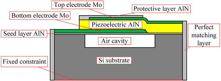
FIGURE 1. 2D model of the FBAR.
TABLE 1. Simulation parameters for the film of the FBAR.
Figure 2 shows the influence of the FBAR structure size on
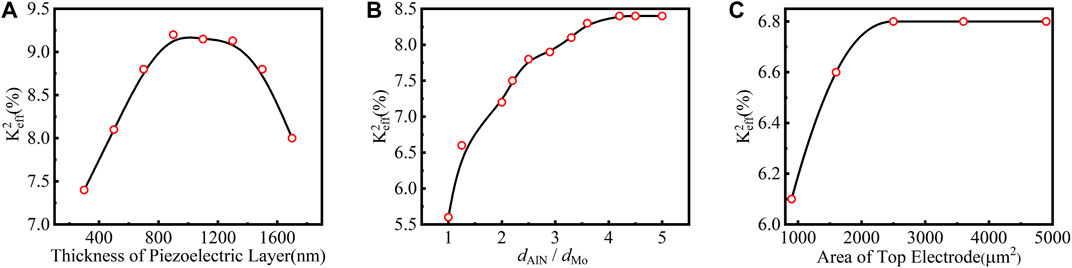
FIGURE 2. (A)
A 3D finite element model was established to analyze the effects of the apodization electrode on the spurious resonance of the FBAR are shown in Figure 3. The material and structural details of this model are the same as those of the 2D model.
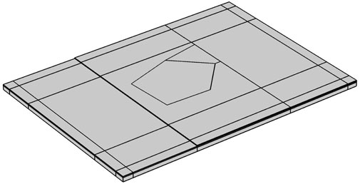
FIGURE 3. 3D finite element model of the FBAR.
The Smith chart is most often used to evaluate the impedance matching and designs of matched networks. Herein, the Smith plot also depicts the unwanted resonances or spurious modes by smaller loops. The influence of different electrode shapes on the spurious resonance of the FBAR was analyzed when the structural parameters were constant, as shown in Figure 4. Compared with rectangular electrodes, the triangular, apodized quadrilateral, circular, and apodized pentagonal electrodes significantly weaken the spurious resonances. This is because the apodized electrodes increases the propagation distance of the transverse Lamb wave to reduce the probability of forming spurious resonance formation by changing the direction of reflection of the transverse Lamb wave. The effects of the apodized pentagonal electrode on spurious resonance suppression was maximal in the simulated structures.
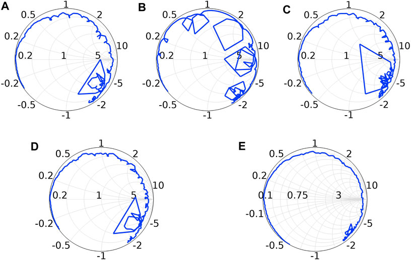
FIGURE 4. Spurious resonances seen in the impedance Smith chart for different shapes of the top electrode: (A) triangle; (B) rectangle; (C) apodized quadrilateral; (D) circle; (E) apodized pentagon.
Table 2 shows the structural optimization parameters of the FBAR. The thickness of the Mo layer of the top electrode is 130 nm and that of the piezoelectric AlN layer is 540 nm. The lattice orientation of the bottom Mo electrode directly affects the quality of the sputtered AlN piezoelectric film. To ensure that the bottom Mo electrode has good sputtered quality, its thickness is selected as 180 nm. The protective and seed layers are 120 and 50 nm thick, respectively. The shape of the top electrode of the FBAR is an apodized pentagon whose area is 3,600 μm2.
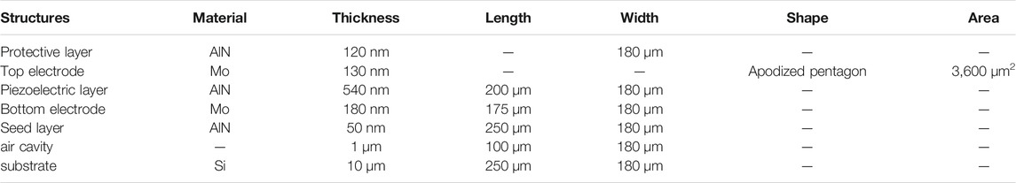
TABLE 2. Structural optimization parameters of the FBAR.
The frequency response of the optimized FBAR is shown in Figure 5. The impedance and phase are observed to vary with frequency, and only small spurious resonances are seen near the parallel resonance point.
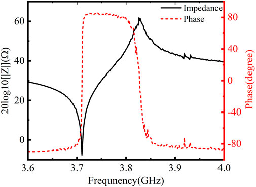
FIGURE 5. Amplitude and phase of Z plotted for the optimized FBAR.
Experimental Fabrication
A prototype FBAR was fabricated using the optimized structural parameters. The fabrication process starts with etching the resonator cavity on a silicon substrate. Thermally oxidized silicon dioxide (SiO2) can protect the substrate when the sacrificial layer is released. Polysilicon is then deposited using PECVD to fill the resonant cavity, next, the seed layer (50 nm) and bottom electrode (180 nm) are sputtered. The former is used to induce the lattice arrangement of the upper film, and the latter is etched to form electrode patterns by ICP-RIE. The piezoelectric layer and top electrode are constructed by sputtering AlN (540 nm) and Mo (130 nm), respectively. The piezoelectric layer should meet the requirements of the c-axis orientation and have high uniformity. Then, the protective layer (120 nm) is sputtered, and the pad layer is deposited by a lift-off process. Finally, the release holes are etched using ICP-RIE, and are distributed around the resonator transducer to release gas into the resonator cavity. Figure 6 shows the fabrication process for a single FBAR.

FIGURE 6. Schematic of the fabrication process of FBAR.
A photograph of the fabricated wafer of the FBAR is shown in Figure 7A. The scanning electron microscope (SEM) image of the cross-section of a single FBAR is shown in Figure 7B. The film quality of each structural layer is observed to meet the requirements, and the sacrificial material in the resonator cavity is completely released.
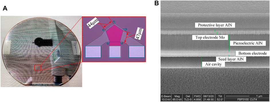
FIGURE 7. Photographs of the fabricated FBAR: (A) wafer; (B) cross section as seen under a SEM.
A microwave probe platform was used to test the fabricated FBAR. Figure 8 shows the performance curve of FBAR. The
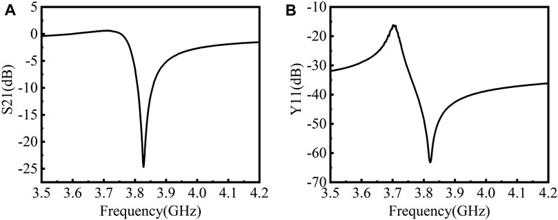
FIGURE 8. Test results of the fabricated FBAR: (A) Transmission coefficient S21; (B) Input admittance Y11.
Comparison and Discussion
A performance comparison between the experimental and simulated FBARs is shown in Table 3. The results of the microwave probe test show that small drifts are observed for the series and parallel resonant frequencies of the FBAR. The
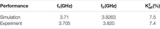
TABLE 3. Performance comparison between experimental and simulated results of the FBAR.
Figure 9 shows the frequency response comparison between the simulated and test data of the FBAR. Compared with the simulation results, there were some small defects near the series resonance point in the test data. However, the simulated results were consistent with the trends of the test data. The main causes of the discrepancies are as follows:
1) The electrode may be oxidized during the fabtrication of the FBAR, thereby increasing its resistivity.
2) During the patterned etching of the electrode, the amount of etching may be too high and may cause defects.
3) Electromagnetic interference during the performance test of the FBAR may cause the observed discrepancies.
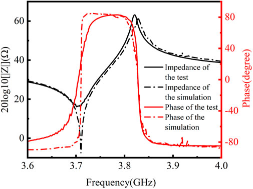
FIGURE 9. Comparison of the test data and simulated data.
The improvement schemes for the above defects may be considered as follows:
1) Optimizing the thin-film sputtering process of the FBAR to prevent oxidation of the electrode during the fabrication process.
2) To reduce or even eliminate the electrode etching defects, the electrode etching process of FBAR may be optimized to improve the accuracy of electrode patterning.
3) The test process may be calibrated and corrected for errors to achieve de-embedding to overcome the influence of the external environment during the measurement process.
Conclusion
In this study, an FBAR was designed and fabricated. Based on 2D and 3D models, the effects of various factors on the performance of FBAR were studied, including the piezoelectric layer thickness, electrode layer thickness, and top electrode area. Using apodization technology, the spurious resonance in the frequency response curve of the FBAR is effectively suppressed. Based on the designed process flow, the FBAR was fabricated, and the SEM image of its cross section exhibited sufficient molded effect. Compared with the simulated results of the FBAR, the frequency response curve was roughly consistent with the trend of the test data, almost achieving the desired performance. Thus, a single FBAR was fabricated with a
Data Availability Statement
The original contributions presented in the study are included in the article/Supplementary Material, further inquiries can be directed to the corresponding authors.
Author Contributions
Conceptualization, CF; methodology, PJ, SM, and ZA; software, ZA, PJ, SM, and ZL; validation, CF, PJ, SJ, LL, TZ, and SM; investigation, PJ, SM, and ZA; resources, CF, SJ, and YY; data curation, SM, PJ, and CF; writing—original draft preparation, PJ and ZA; writing—review and editing, CF, SJ, SM, and LL; fabrication PJ, SM, and SJ; supervision, CF, SJ, and LL; project administration, LL and TZ; funding acquisition, CF, SJ, and YY. All authors have read and agreed to the published version of the manuscript.
Funding
This work was supported by the Key Projects of National Defense Basic Research Program of National Defense Science and Industry Administration (No: JCKY2019210B003) and the Fundamental Research Funds for the Central Universities (No: XJS211105, JBF211103).
Conflict of Interest
Author PJ is employed by the 26th Institute of China Electronics Technology Group Corporation.
The remaining authors declare that the research was conducted in the absence of any commercial or financial relationships that could be construed as a potential conflict of interest.
Publisher’s Note
All claims expressed in this article are solely those of the authors and do not necessarily represent those of their affiliated organizations, or those of the publisher, the editors and the reviewers. Any product that may be evaluated in this article, or claim that may be made by its manufacturer, is not guaranteed or endorsed by the publisher.
References
Bhadauria, A., Panchal, B., and Varghese, S. (2018). “RF Bandpass Filters Using FBAR with Fractal Electrodes,” in 2018 IEEE MTT-S International Microwave and RF Conference (Kolkata, India: IMaRC), 1–3. doi:10.1109/IMaRC.2018.8877300
Bhugra, H., and Piazza, G. (2017). Piezoelectric MEMS Resonators. Berlin, Germany: Springer International Publishing. doi:10.1007/978-3-319-28688-4
Gong, D., Cai, H., Xia, Y., Ma, S., Liu, H., Chiu, Y., and Jin, Y. (2018). “Fabrication and Characterization of AlN Based Piezoelectric Micromachined Ultrasonic Transducer for Contact Sensing,” in 2018 19th International Conference on Electronic Packaging Technology (ICEPT), 1442–1447. doi:10.1109/ICEPT.2018.8480577
Hagelauer, A., Fattinger, G., Ruppel, C. C. W., Ueda, M., Hashimoto, K.-y., and Tag, A. (2018). Microwave Acoustic Wave Devices: Recent Advances on Architectures, Modeling, Materials, and Packaging. IEEE Trans. Microwave Theor. Techn. 66 (10), 4548–4562. doi:10.1109/TMTT.2018.2854160
Hara, M., Yano, Y., Ito, H., Toda, M., Ono, T., Kajita, M., Hara, S., Kasamatsu, A., and Ido, T. (2018). “FBAR Oscillator Stabilized by Rb Atomic Resonator for SHF/EHF-band Wireless Devices,” in 2018 IEEE International Ultrasonics Symposium (Kobe, Japan: IUS), 1–9. doi:10.1109/ULTSYM.2018.8579685
Huang, C. L., Tay, K. W., and Wu, L. (2005). Fabrication and Performance Analysis of Film Bulk Acoustic Wave Resonators. Mater. Lett. 59 (8-9), 1012–1016. doi:10.1016/j.matlet.2004.11.047
Joseph, J., Singh, S. G., and Vanjari, S. R. K. (2018). Piezoelectric Micromachined Ultrasonic Transducer Using Silk Piezoelectric Thin Film. IEEE Electron. Device Lett. 39 (5), 749–752. doi:10.1109/LED.2018.2816646
Kimura, T., Omura, M., Kishimoto, Y., and Hashimoto, K. (2019). Comparative Study of Acoustic Wave Devices Using Thin Piezoelectric Plates in the 3-5-GHz Range. IEEE Trans. Microwave Theor. Techn. 67 (3), 915–921. doi:10.1109/TMTT.2018.2890661
Kirby, P. B., Potter, M. D. G., Williams, C. P., and Lim, M. Y. (2003). Thin Film Piezoelectric Property Considerations for Surface Acoustic Wave and Thin Film Bulk Acoustic Resonators. J. Eur. Ceram. Soc. 23 (14), 2689–2692. doi:10.1016/S0955-2219(03)00147-X
Lakin, K. M., Belsick, J., McDonald, J. F., and McCarron, K. T. (2001). “Improved Bulk Wave Resonator Coupling Coefficient for Wide Bandwidth Filters,” in 2001 IEEE Ultrasonics Symposium. Proceedings. An International Symposium (Cat. No.01CH37263) (Atlanta, GA, USA: IEEE), 827–831. doi:10.1109/ULTSYM.2001.991848
Lee, S., and Mortazawi, A. (2016). “BAW Filter Design Method Based on Intrinsically Switchable Ferroelectric BST FBARs,” in 2016 IEEE MTT-S International Microwave Symposium (San Francisco, CA, USA: IMS), 1–4. doi:10.1109/MWSYM.2016.7540105
Mamishev, A. V., Sundara-Rajan, K., Yang, F., Du, Y., and Zahn, M. (2004). Interdigital Sensors and Transducers. Proc. IEEE 92 (5), 808–845. doi:10.1109/JPROC.2004.826603
Nguyen, N., Johannessen, A., Rooth, S., and Hanke, U. (2019). The Impact of Area on BAW Resonator Performance and an Approach to Device Miniaturization. Ultrasonics 94, 92–101. doi:10.1016/j.ultras.2018.11.014
Schreiter, M., Gabl, R., Pitzer, D., Primig, R., and Wersing, W. (2004). Electro-acoustic Hysteresis Behavior of PZT Thin Film Bulk Acoustic Resonators. J. Eur. Ceram. Soc. 24, 1589. doi:10.1016/S0955-2219(03)00406-0
Stoeckel, C., Meinel, K., Melzer, M., and Otto, T. (2018). “Thin Film Piezoelectric Aluminum Nitride for Piezoelectric Micromachined Ultrasonic Transducers,” in 2018 IEEE SENSORS (New Delhi, India: IEEE), 1–4. doi:10.1109/ICSENS.2018.8589845
Voiculescu, I., and Nordin, A. N. (2012). Acoustic Wave Based MEMS Devices for Biosensing Applications. Biosens. Bioelectron. 33 (1), 1–9. doi:10.1016/j.bios.2011.12.041
Warder, P., and Link, A. (2015). Golden Age for Filter Design: Innovative and Proven Approaches for Acoustic Filter, Duplexer, and Multiplexer Design. IEEE Microwave 16 (7), 60–72. doi:10.1109/MMM.2015.2431236
Zhang, Y., and Chen, D. (2013). Multilayer Integrated Film Bulk Acoustic Resonators. Berlin: Springer.
Zhao, X.-l., Zhao, Z.-n., and Qian, Z.-h. (2019). “Structural Optimization for Uniform Displacement Variations in ZnO FBAR Mass Sensor Using Rectangular Frame-like Driving Electrodes,” in 2019 14th Symposium on Piezoelectricity, Acoustic Waves and Device Applications (Shijiazhuang, China: SPAWDA), 1–4. doi:10.1109/SPAWDA48812.2019.9019224
Keywords: FBAR, effective electromechanical coupling coefficient, AlN thin film, apodization, spurious resonance
Citation: Jiang P, Mao S, An Z, Fei C, Lou L, Li Z, Zhao T, Jiang S and Yang Y (2021) Structure-Size Optimization and Fabrication of 3.7 GHz Film Bulk Acoustic Resonator Based on AlN Thin Film. Front. Mater. 8:731611. doi: 10.3389/fmats.2021.731611
Received: 27 June 2021; Accepted: 05 August 2021;
Published: 20 October 2021.
Edited by:
Jianguo Ma, Beihang University, ChinaReviewed by:
Zhenghua Qian, Nanjing University of Aeronautics and Astronautics, ChinaBo Hou, Soochow University, China
Copyright © 2021 Jiang, Mao, An, Fei, Lou, Li, Zhao, Jiang and Yang. This is an open-access article distributed under the terms of the Creative Commons Attribution License (CC BY). The use, distribution or reproduction in other forums is permitted, provided the original author(s) and the copyright owner(s) are credited and that the original publication in this journal is cited, in accordance with accepted academic practice. No use, distribution or reproduction is permitted which does not comply with these terms.
*Correspondence: Lifei Lou, bG91bGlmZWlAbWFpbC54aWRpYW4uZWR1LmNu; Shiyi Jiang, Mzg1MTc1NjBAcXEuY29t