 Na Li
Na Li Yanwei Tian
 Jianqiang Bao
- Key Laboratory of Electronic Equipment Structure Design, Ministry of Education, Xidian University, Xi’an, China
Compared with the traditional solar cells, the nano-optical antenna breaks through the band-gap limitation of semiconductor materials, and provides a new scheme for solar energy collection. In order to solve the problems of complex structure, low efficiency and narrow bandwidth of nano-optical antenna, a novel nano-ring-cylinder based on metamaterials is proposed in this paper. The antenna has an average absorption efficiency of 96.93% in the wide-band absorption range of visible and near-infrared light. First of all, the basic design theory of the antenna was given based on the surface plasma theory. Then, the antenna structure design scheme was determined, the overall structure consists of two layers of metal and an insulating layer formed by Al2O3. Finally, on the basis of the established antenna model, the absorption characteristics were analyzed by simulation. The analysis result shows that the super-absorption ability of the antenna is independent of the polarization of the incident light, and the average absorption ability can be maintained at about 91% when the incident angle is ±60°. The absorption capability of the antenna is mainly due to the synergistic effect of Fabry-Perot resonance and localized surface plasmon resonance enhancement. The conclusion can provide a theoretical guidance for the structural design of nano-optical antenna.
1 Introduction
Solar energy is one of the most abundant and least polluting renewable resources, so the development of efficient broadband solar absorption device is essential (Hong et al., 2014). At present, solar energy is collected mainly by using solar cells, which work on a photovoltaic effect basis. Because of the limited band gaps of the semiconductor materials, it is difficult to improve the absorption efficiency of solar cells any further. Based on the wave-particle two-phase characteristic of sunlight, some researchers have begun to design nano-scale antennas to receive sunlight which can be considered as a high-frequency electromagnetic wave. Such as nano-dipole (Baldassarre et al., 2015), Slot Yagi nano-antenna (Li M et al., 2019), U shaped nano-antenna (Hubert et al., 2005), bow-tie (Ding et al., 2010), triangular (Xiao et al., 2016) and nano-hole arrays (Du et al., 2011; Jérusalem et al., 2012; Najiminaini et al., 2012).
These nano-optical antenna theoretically has higher absorption efficiency and wider absorbable solar spectral range than solar cells. With the development of material field, the design of nano-optical antenna has more and more broad space. Due to its unique electromagnetic characteristics, the metamaterial has been widely used in the design of solar energy collection devices (Xue and Song, 2021; Li M et al., 2019; Gao et al., 2019; Li Y et al., 2019).
Ming hui (Luo et al., 2017) introduced a new metamaterial nano absorber, which was composed of periodic cylindrical array of nickel (Ni) film. Long Ma et al proposed a periodic Yagi–Uda antenna array to improve the divergence and directivity of the laser beam (Ma et al., 2016). It realized the polarization independent absorption with an average absorption rate higher than 90% in the whole visible region (400–700 nm). Li jun shuai’s team from Nanyang Technological University in Singapore studied the application of the structure of Si nano column plated on Si film in solar energy absorption. Its high absorptivity is concentrated in the shorter wavelength band scope from 300 nm to 400 nm (Li et al., 2009). The University of Chinese Academy of Sciences reported the broadband and efficient light absorption characteristics of a metamaterial sub wavelength nano ring array in the visible region, and the average absorption rate is 97% (Cao et al., 2014). Furthermore, Cao et al. proposed a nano column array based on a complex two-dimensional metamaterial (Cao et al., 2013), with an average absorption rate of 95% in the visible band. However, above studies have mainly focused on the visible or infrared light, and most have complex structures (Yang et al., 2016; Tian and Li, 2016; Yoshikawa et al., 2017; Li and Valentine, 2014). In summary, the introduction of metamaterials provides an effective new solution for the design of nano-optical antennas. Due to the limitation of the current micro-and nano-scale fabrication technology, the antenna structure is too complex to be fabricated. The theoretical study of this nano-optical antenna is much more advanced than the experimental study. The simplification of the structure and the improvement of the performance are the only way to make the nano-optical antenna more practical.
Based on the theory of Surface Plasmon Polaritons (SPS), a kind of feasible nano-ring-cylinder array antenna is designed, in which tungsten is used as the metal layer and alumina is used as the insulating layer. The average absorption rate of the system is up to 96.93%, and it is insensitive to the polarization state of the light.
2 Basic theory of antenna structure design
At present, the Metal-insulator-metal (MIM) metamaterial structures is chosen to absorb the sunlight (Li et al., 2009; Cao et al., 2014; Cao et al., 2013). When the frequency of the incident wave changes, the free electrons in the metal will oscillate collectively, and when the frequency reaches a certain value, the amplitude will reach a peak, which is called surface plasmon effect (Barnes et al., 2003). Surface Plasmon is a kind of electromagnetic wave excited at the junction of medium and metal. It is only affected by the incident wave propagating in the vertical direction. Based on the surface plasmon effect, the wave vector relation between medium and metal is given for transverse magnetic wave TM:
in where
The tangential boundary condition are satisfied as follows:
And
A combination of Formulas (1), (2) and (3)
The surface plasmons dispersion characteristics are related as follows:
in where,
From the above equation, it can be seen that the wave vector of surface plasmon polaritons varies with the metal dielectric constant at different frequencies and has certain dispersion characteristics. Its absorption rate can be calculated as:
where
Based on the above basic theory and the other researchers work (Wang et al., 2017), the highest absorption rate is taken as the design goal, a MIM metamaterial nano-ring-cylinder array antenna with a high dielectric constant imaginary part and refractive index of metallic tungsten was designed. The schematic diagram of the antenna based on micro-metamaterials presented in this paper is shown in Figure 1A. The nano cyclic array is a two-dimensional periodic structure with a 200-nm-thick W/Al2O3 stack on top. The specific structural dimensions are shown in Figure 1. Aluminum oxide has a high refractive index of 1.75 and it is selected as an insulating material. Researchers have found that high refractive index metal (e.g., tungsten) materials are effective in broadening the absorption bandwidth of metamaterial antennas over a range of wavelengths. As seen in the material library of FDTD Solutions, the refractive index of metal W in the 400–1,600 nm band is almost always greater than 2. So this paper chooses tungsten as the metal material of antenna. This MIM nano-ring-cylinder array antenna proposed is fully compatible with standard semiconductor fabrication processes. All layers can be deposited by magnetron sputtering, and then patterned with specific details of the structure by electron beam lithography or focused ion beam.
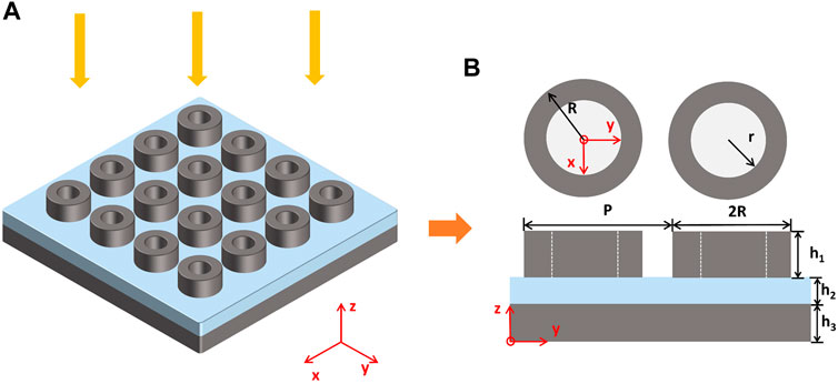
FIGURE 1. (A) Schematic diagram of nano ring array antenna of MIM metamaterial; (B) Cross-sectional view of a single nano ring with W/Al2O3 stack and top view of nano ring.
3 Antenna structure design scheme
The specific structure size of the antenna is determined by the influence of different structure parameters and the absorption efficiency of the antenna. As shown in Figure 2, the paper employs finite-difference time-domain (FDTD) method to analyze the absorption characteristics of MIM nano ring array antenna. Firstly, as shown in Figure 2, the influences of physical dimension to the absorption rate of MIM nano-ring-cylinder array antenna are analyzed in the following study. Figure 2A illustrates the absorptivity against period P of the antenna. The highest average absorptivity is obtained for a 400-nm period. When the period P is larger than 400 nm, the absorptivity becomes worse, which is consistent with previous studies, indicating that the period of the structure is smaller than the wavelength of incident light to avoid scattering. Figure 2B shows the effect of W thickness h1 on the absorptivity. With the increase of h1, the average absorptivity becomes larger. When h1 increases to 160nm, the average absorption rate does not increase significantly. Figure 2C describes the influence of the component of inner radius (r) on absorptivity. Figure 2D shows the effect of the outer radius (R) on the absorptivity. It is found that when r = 80 nm, R = 115 nm the absorptive effect reaches the optimum. When the W layer thickness is close to 130 nm, there is nearly no transmission in the optical regime and light can only be absorbed or reflected by this structure because of the existence of the alternatively layered W thin film. The periodic of the nano-ring pillar array is set to 400 nm. For a single nano ring, its thickness h1 = 160 nm, outer diameter R = 115 nm, inner diameter r = 80 nm, as shown in Figures 1B,C. The substrate is composed of medium Al2O3 and metal W, the thickness of medium h2 = 70 nm, the thickness of metal h3 = 130 nm.
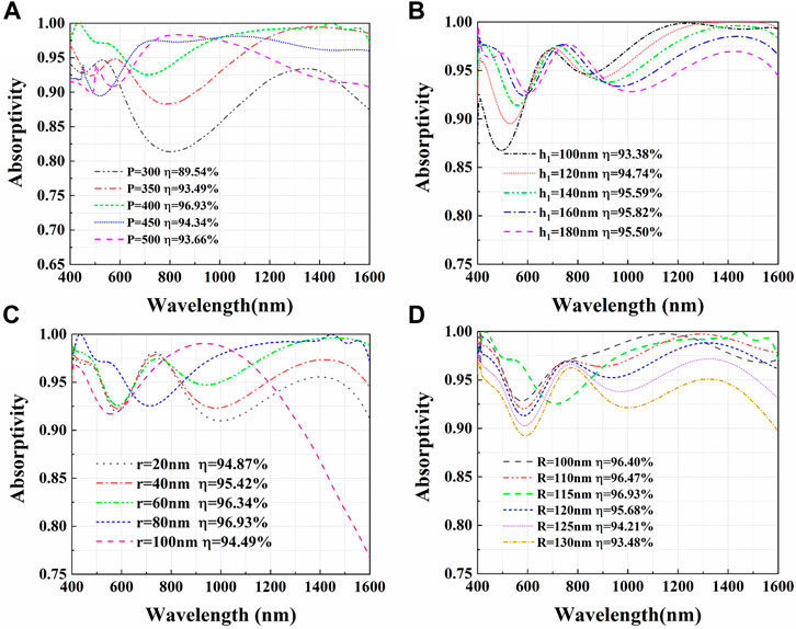
FIGURE 2. Absorption spectra of the MIM nano ring array antenna under normal incident light for various conditions. (A) for different periodicity P when h1 = 160 nm, r = 80 nm, R = 115 nm; (B) for different h1 when P = 400 nm, r = 80 nm, R = 115 nm; (C) for different r when P = 400 nm, h1 = 160 nm, R = 115 nm; (D) for different R when P = 400 nm, h1 = 160 nm, r = 80 nm.
4 Performance improvement method of absorptivity
In order to find an effective method to improve the absorptivity of the nano-ring-cylinder array antenna, effect of the relative factors on the absorptivity is analyzed.
4.1 Relationship between the absorptivity and incident light
In order to fully describe the relationship between the absorptivity of sub nano-ring-cylinder array and incident light, the state and incident angle of incident light are analyzed and calculated. Figures 3A,B show the absorptive spectra at various incident angles for TE and TM wave, respectively. Although the absorptivity decreases at 550 nm wavelength, the average absorptivity retains a value up to 91% over a wide incident angle of ±60° and ±40° for both TE and TM polarization, respectively. Such results show that our nano-ring-cylinder structure is insensitive to the form and angle of incident light.
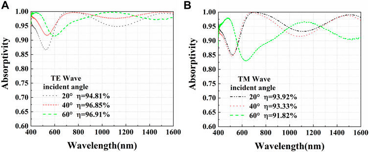
FIGURE 3. Absorption spectra of MIM nano ring array antenna under various conditions. (A) different incident angles of 20°, 40° and 60° for a TE wave; (B) different incident angles of 20°, 40° and 60° for a TM wave.
To gain a better understanding of the absorption mechanism, the electric field in x–z plane at y = 0 distribution |Ex| for different incident wavelengths is calculated and shown in Figure 4. The hotspot of the concentrated electric field is located at the edge of the nano-ring-cylinder. The localized surface plasmon enhancement effect results in the hotspot’s appearance. As can be seen from Figure 4, the electric field intensity at the edge of the nano ring is enhanced. The reason is that the surface plasmon propagates only along the W interface. When the incident wavelength is less than 700 nm, in Figures 4A–C, the hot spots are located at the edges of the nano-ring-cylinder, mainly at the upper and right sides, and the electric field intensity is gradually enhanced at the upper and lower edges of the nano-ring-cylinder with increasing wavelength. This implies that the surface plasmon resonance occurs mainly on the nano-ring-cylinder and the electric field on the structure is enhanced. In contrast, in Figures 4D–F, when the incident wave grows longer than 700 nm, the hot spot of the concentrated electric field is almost at the edge of the contact with Al2O3 and the nano ring almost lose its function. At this time, the surface plasmon resonance occurs mainly at the place where the nano-ring-cylinder are in contact with Al2O3. Especially at the wavelength of 1,600 nm, the electric field is almost entirely concentrated at the contact between the nano-ring-cylinder and Al2O3, and the electric field intensity reaches up to 6 V/m.
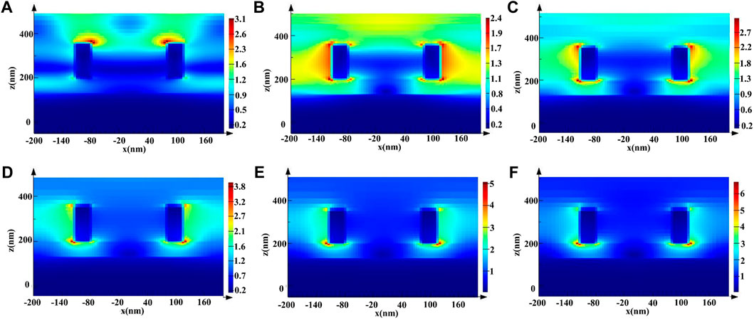
FIGURE 4. Electric field Ex distribution at y=0 plane for different-wavelengths.*(A) λ = 400 nm; (B) λ = 600 nm; (C) = 700 nm; (D) λ = 1000 nm; (E) λ =1300 nm; (F) λ =1600 nm.
4.2 Relationship between the absorptivity and surface plasmon resonance effect
In addition, the electric field in x–y plane at z = 200 nm and z = 360 nm distribution |Ex| for different incident wavelengths is calculated and shown in Figure 5. From Figure 5, it is shown that the hotspots of the concentrated electric field at the bottom of the nano-ring-cylinder is very strong. These hotspots can be attributed to the surface plasmon resonance. The free electrons in the metal material resonate with the incident light, and then the surface plasmon polaritons are generated and propagated along the surface of the metal and medium. Therefore, the electric field intensity is enhanced at the bottom of the nano ring.
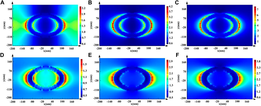
FIGURE 5. Electric field in x-y plane for different wavelengths. (A) z = 200 nm, λ =560 nm, (B) z = 200 nm, λ = 1060 nm, (C) z = 200 nm, λ = 1600 nm, (D) z = 360 nm, λ =560 nm. (E) z = 360 nm, λ =1060 nm, (F) z = 360 nm. λ = 1600 nm.
To further find out the absorbing mechanism from other aspects, we investigate the y-component of the normalized magnetic field distribution |Hy| in the plane of y = 0 at different wavelengths, as shown in Figure 6. With the increase of the wavelength, the magnetic energy flow converges slowly, and the dielectric layer Al2O3 is the strongest distribution position of the magnetic field |Hy|. As shown in Figures 6B,C, strong magnetic fields are confined in the dielectric gap between the top metal disks and the bottom metal film, which are typical magnetic resonances contributing to high absorption. The electromagnetic field is mainly concentrated in the medium between the upper metal film and the lower thick metal layer. There is a parallel reverse current between the two layers. This is because there is a parallel reverse current between the upper metal array and the lower thick metal. Its current can form a displacement current circuit between the upper and lower metals. This displacement current circuit interacts with the incident electromagnetic field to produce magnetic moment. As shown in Figure 6A, at 560 nm wavelength, the strong magnetic field is limited to the interface between the dielectric and the bottom metal film, which indicates that a typical antireflective resonance is generated. When a quarter-wavelength incident light strikes a metal film, the reflected electric field from the surface of the metal exhibits a phase opposite to the incident electric field. Therefore, the two cancel each other in the thin film media, resulting in a sharp decline in reflectivity. It is also proved that the absorption rate decreases at about 550 nm. Moreover, the resonance formed at the wavelength of 1600 nm is further analyzed, the analysis found that the Fabry-Perot (F-P) resonance leads to the occurrence of this phenomenon. The period of the F-P resonance at λ = 1,600 nm was calculated to be 400 nm by FDTD methods, and the effective refractive index of the MIM nano ring antenna array was
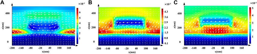
FIGURE 6. The normalized magnetic field distribution Hy in the plane of y = 0 at different wavelengths. (A) λ = 560 nm: (B) λ = 1000 nm: (C) λ = 1600 nm.
5 Conclusion
In this paper, a metal-insulator-metal (MIM) nano-ring-cylinder array absorption antenna based on metamaterial is proposed. The antenna has a simple structure, while achieving a higher absorption rate of 96.93% in the 400–1600 nm band. The simulation results demonstrate that the antenna is insensitive to the light polarization state and retain the average absorptivity of 91% at a very large incident angle of ±60°. Compared with the nano ring column array absorber reported in reference (Cao et al., 2014), the antenna proposed has a significant advantage in high absorptivity in broadband. This high light absorptivity of the MIM nano ring array antenna can be explained as the synergetic effect of Fabry–Perot resonance as well as localized plasmonic resonance enhancement. The proposed MIM nano-ring-cylinder array antenna is fully compatible with standard semiconductor manufacturing processes. With the vast demand for sustainable and green energy, we believe that the structure proposed in this paper will be applied in the fields related to solar energy collection.
Data availability statement
The raw data supporting the conclusions of this article will be made available by the authors, without undue reservation.
Author contributions
Author Contributions: NL: Direction control and article revision. NL and YT: Investigation, Data curation, Writing- Original draft preparation. JB and YW: Software, Validation. CZ: Conceptualization, Methodology, Supervision. YT and CZ: Software, Conceptualization, Methodology, Supervision. NL, JB and YW: Conceptualization, Methodology, Writing- Reviewing and Editing.
Funding
The authors acknowledge the financial supports from the National Natural Science Foundation of China under Grant U1931139.
Conflict of interest
The authors declare that the research was conducted in the absence of any commercial or financial relationships that could be construed as a potential conflict of interest.
Publisher’s note
All claims expressed in this article are solely those of the authors and do not necessarily represent those of their affiliated organizations, or those of the publisher, the editors and the reviewers. Any product that may be evaluated in this article, or claim that may be made by its manufacturer, is not guaranteed or endorsed by the publisher.
References
Baldassarre, L., Sakat, E., Frigerio, J., Samarelli, A., Gallacher, K., Calandrini, E., et al. (2015). Midinfrared plasmon-enhanced spectroscopy with germanium antennas on silicon substrates. Nano Lett. 15, 7225–7231. doi:10.1021/acs.nanolett.5b03247
Barnes, W. L., Dereux, A., and Ebbesen, T. W. (2003). Surface plasmon subwavelength optics. nature 424, 824–830. doi:10.1038/nature01937
Cao, S., Yu, W., Wang, T., Xu, Z., Wang, C., Fu, Y., et al. (2013). Two-dimensional subwavelength meta-nanopillar array for efficient visible light absorption. Appl. Phys. Lett. 102, 161109. doi:10.1063/1.4803046
Cao, S., Yu, W., Zhang, L., Wang, C., Zhang, X., and Fu, Y. (2014). Broadband efficient light absorbing in the visible regime by a metananoring array. Ann. Phys. 526, 112–117. doi:10.1002/andp.201300198
Ding, W., Bachelot, R., Kostcheev, S., Royer, P., and Espiau de Lamaestre, R. (2010). Surface plasmon resonances in silver Bowtie nanoantennas with varied bow angles. J. Appl. Phys. 108, 124314. doi:10.1364/QELS.2011.QTuH1
Du, Q. G., Kam, C. H., Demir, H. V., Yu, H. Y., and Sun, X. W. (2011). Enhanced optical absorption in nanopatterned silicon thin films with a nano-cone-hole structure for photovoltaic applications. Opt. Lett. 36, 1713–1715. doi:10.1364/OL.36.001713
Gao, E., Liu, Z., Li, H., Xu, H., Zhang, Z., Zhang, X., et al. (2019). Dual plasmonically induced transparency and ultra-slow light effect in m-shaped graphene-based terahertz metasurfaces. Appl. Phys. Express 12, 126001. doi:10.7567/1882-0786/ab5602
Hong, L., Wang, X., Zheng, H., He, L., Wang, H., Yu, H., et al. (2014). High efficiency silicon nanohole/organic heterojunction hybrid solar cell. Appl. Phys. Lett. 104, 053104. doi:10.1063/1.4863965
Hubert, C., Rumyantseva, A., Lerondel, G., Grand, J., Kostcheev, S., Billot, L., et al. (2005). Near-field photochemical imaging of noble metal nanostructures. Nano Lett. 5, 615–619. doi:10.1021/nl047956i
Jérusalem, A., Fernández, A., Kunz, A., and Greer, J. R. (2012). Continuum modeling of dislocation starvation and subsequent nucleation in nano-pillar compressions. Scr. Mater. 66, 93–96. doi:10.1016/j.scriptamat.2011.10.009
Li, J., Yu, H., Wong, S. M., Zhang, G., Sun, X., Lo, P. G.-Q., et al. (2009). Si nanopillar array optimization on Si thin films for solar energy harvesting. Appl. Phys. Lett. 95, 033102. doi:10.1063/1.3186046
Li, M., Liang, C., Zhang, Y., Yi, Z., Chen, X., Zhou, Z., et al. (2019). Terahertz wideband perfect absorber based on open loop with cross nested structure. Results Phys. 15, 102603. doi:10.1016/j.rinp.2019.102603
Li, W., and Valentine, J. (2014). Metamaterial perfect absorber based hot electron photodetection. Nano Lett. 14, 3510–3514. doi:10.1021/nl501090w
Li, Y., Liu, Z., Zhang, H., Tang, P., Wu, B., and Liu, G. (2019). Ultra-broadband perfect absorber utilizing refractory materials in metal-insulator composite multilayer stacks. Opt. Express 27, 11809–11818. doi:10.1364/OE.27.011809
Luo, M., Shen, S., Zhou, L., Wu, S., Zhou, Y., and Chen, L. (2017). Broadband, wide-angle, and polarization-independent metamaterial absorber for the visible regime. Opt. Express 25, 16715–16724. doi:10.1364/oe.25.016715
Ma, L., Lin, J., Ma, Y., Liu, B., Tan, J., and Jin, P. (2016). Yagi–Uda optical antenna array collimated laser based on surface plasmons. Opt. Commun. 368, 197–201. doi:10.1016/j.optcom.2016.01.090
Najiminaini, M., Vasefi, F., Kaminska, B., and Carson, J. J. (2012). Effect of surface plasmon energy matching on the sensing capability of metallic nano-hole arrays. Appl. Phys. Lett. 100, 063110. doi:10.1063/1.3683536
Tian, X., and Li, Z.-Y. (2016). Visible-near infrared ultra-broadband polarization-independent metamaterial perfect absorber involving phase-change materials. Photonics Res. 4, 146–152. doi:10.1364/PRJ.4.000146
Wang, W., Qu, Y., Du, K., Bai, S., Tian, J., Pan, M., et al. (2017). Broadband optical absorption based on single-sized metal-dielectric-metal plasmonic nanostructures with high-ε ″metals. Appl. Phys. Lett. 110, 101101. doi:10.1063/1.4977860
Xiao, S., Wang, T., Liu, Y., Xu, C., Han, X., and Yan, X. (2016). Tunable light trapping and absorption enhancement with graphene ring arrays. Phys. Chem. Chem. Phys. 18, 26661–26669. doi:10.1039/C6CP03731C
Xue, Y., and Song, Z. (2021). Nano-efficient photoelectric conversion-based solar photovoltaic system and its usage in green buildings. J. Nanoelectron. Optoelectron. 16, 264–272. doi:10.1166/jno.2021.2956
Yang, C., Ji, C., Shen, W., Lee, K.-T., Zhang, Y., Liu, X., et al. (2016). Compact multilayer film structures for ultrabroadband, omnidirectional, and efficient absorption. Acs Photonics 3, 590–596. doi:10.1021/acsphotonics.5b00689
Keywords: solar energy harvesting, metamaterial, metal-insulator-metal, broadband, surface plasmon resonance
Citation: Li N, Tian Y, Bao J, Wang Y and Zhao C (2022) Design of broadband high efficiency absorption antenna based on metamaterial nano-ring array. Front. Mater. 9:1012936. doi: 10.3389/fmats.2022.1012936
Received: 06 August 2022; Accepted: 23 August 2022;
Published: 19 October 2022.
Edited by:
Zongliang Du, Dalian University of Technology, ChinaReviewed by:
Jiachen Luo, Dalian University of Technology, ChinaXiaopeng Li, Toyota Research Institute of North America, United States
Copyright © 2022 Li, Tian, Bao, Wang and Zhao. This is an open-access article distributed under the terms of the Creative Commons Attribution License (CC BY). The use, distribution or reproduction in other forums is permitted, provided the original author(s) and the copyright owner(s) are credited and that the original publication in this journal is cited, in accordance with accepted academic practice. No use, distribution or reproduction is permitted which does not comply with these terms.
*Correspondence: Na Li, bGluYUBtYWlsLnhpZGlhbi5lZHUuY24=