 Bhanu Priya1Priya Jasrotia1Arun Kumar2Vinamrita Singh3Jehova Jire L. Hmar3Raj Kumar4
 Pawan Kumar Kulriya5
 Tanuj Kumar1*
- 1Department of Nanoscience and Materials, Central University of Jammu, Jammu, India
- 2Department of Physics, J.C. Bose University of Science and Technology, YMCA, Faridabad, India
- 3Department of Physics, Netaji Subhas University of Technology, Delhi, India
- 4Inter University Accelerator Centre, Aruna Asif Ali Marg, New Delhi, India
- 5Department of Physical Sciences, Jawaharlal Nehru University, New Delhi, India
This report investigates the effect of substrate and nitrogen (16 keV N+) ion implantation on the structural, morphological, compositional, and electrical properties of V2O5 thin films which are grown by thermal evaporation on various substrates, including glass, Si, and sapphire (termed V2O5:Gl, V2O5:Si, and V2O5:Sp, respectively). Structural analysis showed the formation of the mixed (α, and β-V2O5) phases on all substrates; however, the β-V2O5 phase is highly dominant in the V2O5:G and V2O5:Si samples. A deformation in the β-phase of V2O5 thin film under ion implantation-induced strain results in a change of crystallite size. Irradiation suppresses XRD peaks in relative intensities, indicating partial amorphization of the film with defect formation. Microstructural analysis confirmed the formation of uniform-sized nanorods for V2O5:Si, whereas isolated crystallites were formed for other types of substrates. Thermal conductivity may influence the size and shapes of V2O5 crystallite forms on different surfaces. Silicon absorbs heat more effectively than sapphire or glass, resulting in nanorod formation. A decrease in optical bandgap and electrical conduction has been observed due to increased oxygen vacancies, induced electron scattering, and trapping centres on N+ implantation. The present study thus offers the unique advantage of simultaneous reduction in optical band-gap and conductance of V2O5 thin films, which is important for optoelectronic applications.
Introduction
In the last few years, studies on the synthesis and modification of the properties of vanadium oxides have gained scientific interest due to their potential applications in electrochemical activity, thermochromics (Wei et al., 2015; Kumar et al., 2017), optics (Lu et al., 2012; Arbab and Mola, 2016), and electronics (Rao, 2013; Majumdar et al., 2019). Out of various phases of vanadium oxide (VO2, V2O3, V2O5, V3O7 etc.), V2O5 is the most stable with a wide band gap energy of Eg = 2.2–2.3 eV in its bulk form (Kenny et al., 1966). Depending on the structural stability of V2O5 under different growth mechanisms, V2O5 can exist in several polymorphs including orthorhombic α-V2O5 (Enjalbert and Galy, 1986), tetragonal or monoclinic β-V2O5 (Volkov et al., 1988; Filonenko et al., 2004), and orthorhombic γ-V2O5 (Cocciantelli et al., 1991). Thin films with high surface-to-volume ratios created by the nanometric scaling of bulk materials have fascinating functional features that differ from their bulk counterparts. Nano- and micro-structures in V2O5 thin film result in an unusual morphology, with materials that physically and chemically differ from bulk materials.
Various physical and chemical routes can synthesize V2O5 thin films, such as physical vapour deposition (PVD), sputtering, hydrothermals, sol-gel, spray-pyrolysis, and spin coating. The structural and morphological properties of thin films critically depend on the process of synthesis and the substrate used. On quartz, Si, and alumina, V2O5 films were deposited using the sol-gel approach, whereas amorphous V2O5 films were created on glass substrates (Khan et al., 2015). Both α-V2O5 and β-V2O5 phases on the films were observed simultaneously using the sol-gel technique on Si and glass substrates, respectively, under the same experimental conditions. Using the sol-gel process for thin film deposition on both quartz glass and silicon substrates also revealed a heterogeneous structure of α and β phases of V2O5 (PrzeVniak-Welenc et al., 2015). Out of these various methods, the physical vapour deposition technique of thermal evaporation is an effective approach for synthesising quality films with good uniformity and porosity (Beke, 2011) over a large surface area when properly controlled.
Numerous V2O5 nanostructures—including nanowires, nanotubes, and nanosheets—have been extensively studied in the last 10 years as possible functional materials for lithium-ion batteries (Kim and Ahn, 2006; Liu et al., 2011). In the literature, the change of thickness and/or doping of V2O5 films with cations (transition metal, boron, etc.) results in the tuning of structural strength, optical band gap, and electrical properties. Different functional properties of V2O5 thin films after metal doping—such as Ag (Hwang et al., 2004), Mo (Jin et al., 2009), Sn (Li et al., 2013), Zr (Zhang et al., 2014), Na (El Desoky et al., 2014), F (RezaBenama et al., 2015), Cu (Yu et al., 2013), and Cr (Zhan et al., 2009)—using various methods are well reported. For instance, the improved electrochemical properties of V2O5 have been observed after Cu doping (Coustier et al., 1999), whereas Ag enhanced the electrical properties (Couster et al., 1997). As per previous studies, doping with transition metals provides the narrowing band gap in wide-band-gap semiconductors (Jovanovic et al., 2018). Negreira and Wilcox (2011) have shown that the surface reactivity of V2O5 (001) is governed by oxygen vacancies by lowering the band gap. Narrowing the bandgap using doping during the synthesis of V2O5 favours increased conductivity and, hence, has the limitation of independent control over bandgap and electrical conduction. These approaches are also limited by incorporating gaseous dopants.
Ion implantation using accelerators offers the doping of V2O5 films with independent control over the tuning of the optical bandgap and electrical conduction. Ion implantation can induce crystalline imperfections and oxygen defects in near-surface of V2O5 films through the preferential sputtering of lighter O atoms. In general, oxygen vacancies and ion implantation (at interstitial or substitution sites) act as trapping or scattered centres for conducting electrons inside the materials. Moreover, oxygen vacancies favour the lowering of the optical bandgap. Here, the experimental work has been designed to simultaneously lower the bandgap of V2O5 and their electrical conduction using N+ ion implantation. To the best of our knowledge, the influence of the substrate on the optical bandgap, phase structure, and electrical properties of V2O5 films as a function of ion implantation has rarely been reported.
Experiment
A standard procedure was used to clean the surfaces of different substrates: glass, n-Si (100), and sapphire using alcohol and acetone. Thence, a uniform V2O5 thin film (t ∼ 500 nm) was grown on the various types of substrates termed V2O5:Gl, V2O5:Si, and V2O5:Sp using a thermal evaporator system with a base pressure of 1 × 10⁻⁶ bar and a rotating target holder. The re-crystallization of V2O5 was performed by heating it at 500°C for 6.5 h. The 16 keV N+ ion implantation at a fluence of 5 × 10¹² and 1 × 10¹⁴ ions/cm2 into crystallised V2O5 thin films was carried out using an indigenously made tabletop accelerator at the Inter-University Accelerator Centre, New Delhi, India. The structural phase analysis of the pristine and implanted samples was carried out with the aid of an X-ray diffractometer Rigaku Miniflex 600 by using a Cu Kα radiation source (λ = 1.5406 Å) operated at 40 kV and 20 mA. The FTIR analysis was carried out using Shimadzu IR infinity in KBR mode in the 400–4000 cm−1 range. A field emission scanning electron microscope (FESEM) was used to characterize the surface morphology of thin films (JSM 7610F Plus, JEOL). The optical characteristics and band gap of the thin films were examined using a UV-VIS-NIR spectrophotometer (Model-Shimadzu 3600i Plus). The electrical conductivity of these samples was assessed using the Keithley source meter 2450 apparatus at the Central University of Jammu, Jammu.
Results and discussion
X-ray diffraction study
Figures 1A–C show the XRD patterns of V2O5 500 nm-thin films deposited on glass, sapphire, and silicon (V2O5:Gl, V2O5:Sp, and V2O5:Si, respectively), followed by thermal annealing at 500°C for 6.5 h and then subsequent implantation with 16 keV N+ at fluence 5 × 10¹² and 1 × 10¹⁴ ions/cm2. All the samples are found to be polycrystalline in nature, and their diffraction peaks seem to be dominated by the β-V2O5 tetragonal phase (Pmmn space group, JCPDS card No.00-045-1074) in V2O5:Gl, V2O5:Si, and α-V2O5 orthorhombic phase (Pmmn space group, JCPDS card No. 01-089-2482) in V2O5:Sp. In the case of the annealed V2O5: Gl thin film, diffraction peaks of β-V2O5 appeared at the 2θ values of ∼12.58°, 18.44°, and 28.53°, which correspond to the (200), (221), and (033) planes, with additional peaks of α-V2O5 at angles 15.28° and 20.25° representing the (200) and (001) crystallographic planes. Thus, a mixture of α-V2O5 and β-V2O5 phases is observed in annealed V2O5:Gl thin films. In the enlarged view of the V2O5:Gl XRD pattern in Figure 1D, it is evident that the 12.5° peak corresponding to β-V2O5 is highly dominant compared with the sapphire and silicon samples. The peak is oriented along the surface, and the relative intensity is found to decrease with an increase in ion fluence from 5 × 10¹² to 1 × 10¹⁴ ions/cm2, respectively, indicating the degradation of its crystalline nature. The enlarged view of V2O5:Sp shows that the 15.3° peak representing α-V2O5 (200) is dominant and its relative intensity decreases ion fluence. In the case of V2O5:Si, peak intensity has been observed at 20.3° belonging to α-V2O5 for the pristine and all irradiated films. The XRD patterns of the V2O5 samples that were irradiated with N+ produced results that were distinct from those of the annealed sample, both in terms of the relative intensities of the peaks and the positions they held. A minor and continuous narrowing of the interplanar gap—the shift of the peak’s position to higher angles—has been observed. Similar gradual shifts are observed for the other peaks as well. The suppression of peak intensity is the maximum for the sample implanted at a higher fluence of 1 × 10¹⁴ ions/cm2. Suppression in peak intensities is due to the deformation of crystal structure by the production of defects (O, V-vacancies) with 16 keV N+ ion implantation, as discussed in the following sections.
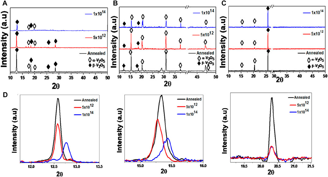
FIGURE 1. XRD pattern of the V2O5 thin film deposited on glass, sapphire, and silicon substrates, respectively, before and after irradiation: (A) V2O5:Gl; (B) V2O5:Sp; (C) V2O5:Si; (D) corresponding zoom images of XRD patterns at respective 2θ values for each substrate.
Analysis of XRD shows variation in grain size with ion fluence. The annealed V2O5:Gl film has a mean grain size of about 62 nm according to the Debye-Scherrer formula, while samples treated with N+ have grain sizes of 64 nm and 51 nm, respectively. The calculated values of the grain size for the V2O5:Sp samples are 54.4 nm, 54 nm, and 52 nm for annealed V2O5 5 × 10¹² and 1 × 10¹⁴ ions/cm2 N+ implanted samples, whereas 45 nm, 56 nm, and 52 nm are the respective grain size values for V2O5:Si after annealing and implantation. Micro-strain is calculated using the WH plot for all three substrates. According to Debye Scherrer’s formula,
where D is the crystallite (grain) size, β is the full width at half maximum (FWHM) of a diffraction peak with θ angle, λ = 1.54056 Å is the X-ray wavelength, and ε is the micro-strain parameter.
The W-H plot—βcosθ against 4sinθ—for V2O5:Gl annealed and also after implantation with N+ at fluencies 5 × 10¹² and 1 × 10¹⁴ ions/cm2 are given in Figure 2. The positive slope of the WH plots shows that the synthesized particles have tensile strains. In Table 1, the values for the intercept and slope following linear fitting of the plots—which define the crystallite size and lattice microstrain, respectively—are shown. As can be seen, crystallite size increases initially with N+ fluence and then exhibits a slight fluctuation as fluence increases. It appears that N+ ions help V2O5 thin films form grains more easily. Using the relation
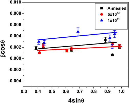
FIGURE 2. W-H plot (βcosθ against 4sinθ) for the V2O5:Gl matrix.
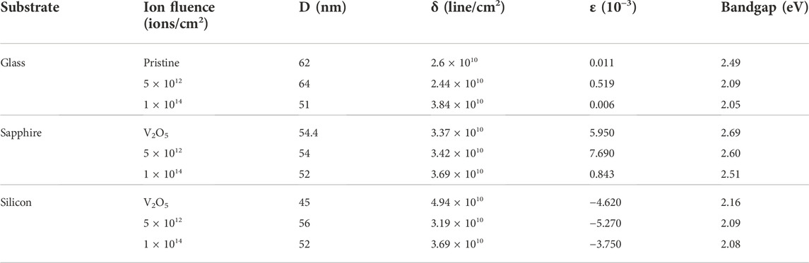
TABLE 1. Crystallite size (D), lattice microstrain (ε), dislocation density (δ), and band gap values (Eg) of V2O5 thin films on glass, sapphire, and silicon substrates.
FTIR analysis
Figure 3 depicts the Fourier-transfer infrared spectra of N + -implanted V2O5:Gl, following heat treatment (500°C for 6.5 h) and at fluences of 5 × 10¹² and 1 × 10¹⁴ ions/cm2. The structural determination of orthorhombic V2O5 is clearly shown by the peak location of the vanadyl mode (vanadium oxygen double bond, V=O) for all samples: 1027 cm−1. The IR band of V=O is often seen around 1017–1021 cm−1 (Legrouri et al., 1993; Metin et al., 2008; Eric Kumi-Barimah et al., 2020) in crystalline V2O5. The bending vibration of the V-O-V bond is represented as a peak at roughly 504 cm−1 in the annealed sample at 500°C (Legrouri et al., 1993; Metin et al., 2008). Additionally, the symmetric (s: V-O-V) and asymmetric (as: V-O-V) stretching bonds are responsible for the other two large peaks at around 760 cm−1 and 867 cm−1, respectively. With the N-O stretch region spanning 1475 to 1550 cm-1, the IR peak of symmetric N-O stretch occurs at 1511 cm−1. The symmetric stretching of V-O-V, whose peaks are seen between 400 and 700 cm−1, moves to the lower wave numbers and combines with the bending V-O-V peak to create a single peak at the lower frequencies. In addition, the strength of V-O-V and V=O bonds in the annealed V2O5:Gl sample is greater than in the N+ implanted sample; this strength decreases with increasing ion fluence, suggesting that the annealed sample is more crystalline. Bond assignments and FT-IR peak positions for the samples are shown in Table 2.
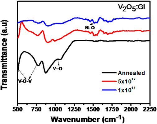
FIGURE 3. FTIR spectra of V2O5:Gl thin films after annealing and ion implantation at different fluences.
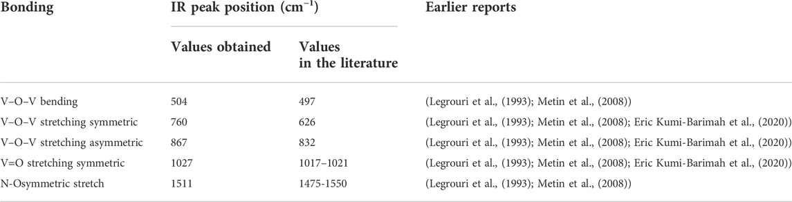
TABLE 2. Infrared peak positions and bond attributions in comparison with earlier reports.
Morphological studies
Figures 4A–G show the FESEM images of annealed and N+ implanted (1 × 10¹⁴ ions/cm2) V2O5 thin films on the glass substrate (V2O5:Gl) and their elemental composition analysis using EDS. For the annealed sample, the development of crystallites of different shapes and sizes can be seen on the smooth and uniform film surface in Figure 4A. The resulting film is non-homogeneous and contains surface agglomerations, while the crystallites of V2O5 are uniformly distributed over the surface of V2O5:Gl ( Figure 4B), demonstrating the presence of crystallites that are less compact and scattered over the surface with surface adhesion. On this film’s surface, there are a few fractures between the spaces of crystallites that may have formed as a result of material shrinkage during the annealing process. A magnified image in Figure 4C shows the crystallite nature of particles in the form of pyramid and dipyramid shapes of orthorhombic and/or tetragonal structures. A higher magnification has been presented in 4 (d), where the crystallites marked as ‘1’ and ‘2’ are dipyramids and the crystallite ‘3’ is a mono-pyramid, which supports the findings of orthorhombic and/or tetragonal structures observed through the XRD study. In Figure 4G, the size distribution of crystallites shows the average diameter of 56.9 nm for N+ implanted V2O5:Gl at a fluence of 1 × 10¹⁴ ions/cm2. Eric Kumi-Barimah et al. (2020) explained that the sample’s whole substrate surface is covered in V2O5 crystallites or grains of various sizes that are randomly distributed and increase in size with an increase in the substrate temperature. In the present work, it is observed that sputtering of the surface and changing surface composition cause the crystallite size to decrease, following irradiation. To map the elemental surface composition, the EDS spectra of corresponding V2O5 thin films of annealed and irradiated 1 × 10¹⁴ ions/cm2 have been recorded and are shown in Figures 4E and F, respectively. The corresponding insets show the colour mapping of the elemental overlay of N, V, and O, which are uniformly distributed, in the thin films before and after irradiation. In EDS spectra, the presence of Lα and Kα is visible for the elements vanadium (V) and oxygen (O). The presence of Ca, Na, and Si correspond to the composition of the glass substrate. Irradiation at 1 × 10¹⁴ ions/cm2 results in an atomic percentage of 4% nitrogen (N) inside the near-surface of the V2O5 thin film. Figure 4G shows the particle size distribution of V2O5 thin film at 1 × 10¹⁴ ions/cm2 fluence on glass substrate.
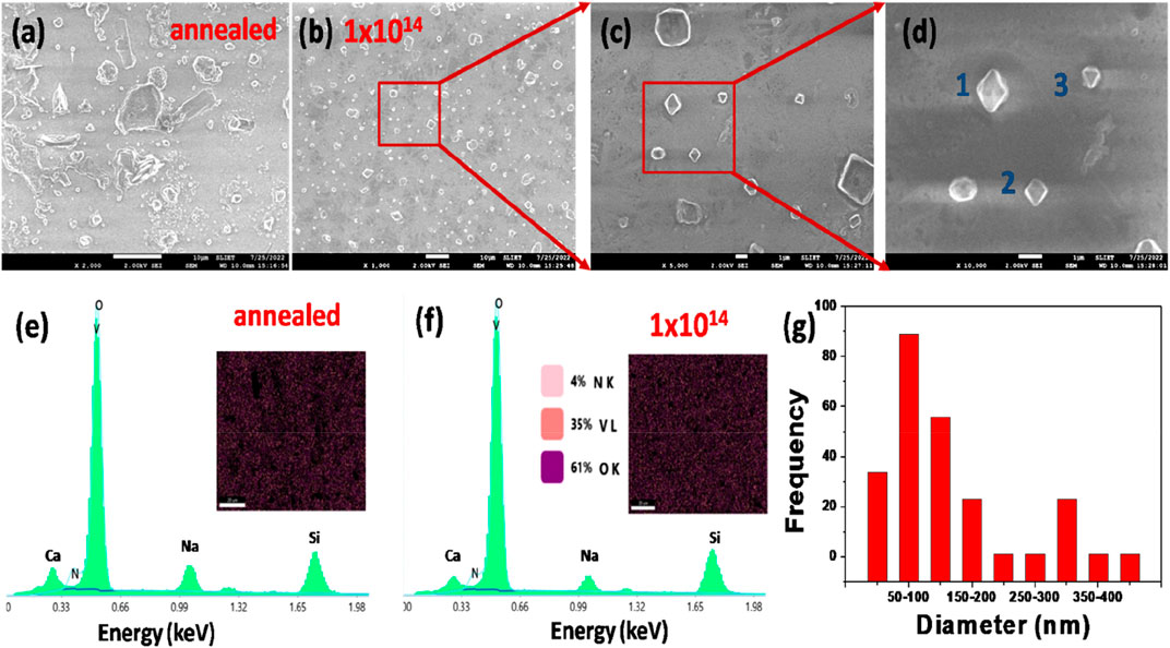
FIGURE 4. FE-SEM images and the crystallite size distribution of V2O5 thin films on the glass substrate (A) annealed, (B) after irradiation with N+ at 1 × 10¹⁴ ions/cm2, (C) and (D) are the corresponding zoomed images of (B), (E) EDS spectra of annealed (F) EDS spectra of V2O5 thin film at 1 × 10¹⁴ ions/cm2 fluence, (G) particle size distribution of V2O5 thin film at 1 × 10¹⁴ fluence.
In the case of the V2O5:Si matrix, FESEM images show the formation of V2O5 nanorods which are randomly distributed over the surfaces for annealed and N+ implanted (at 1 × 10¹⁴ ions/cm2) samples, as shown in Figures 5A and B, respectively. Nanorod formation is seen on these samples with an average diameter of 142 nm for pristine and 304 nm for the film at fluence 1 × 10¹⁴ ions/cm2. However, it is notable that the diameter of the nanorods is more than the crystallite sizes obtained from the XRD data. EDS spectra and the insets in Figures 5C and D show the elemental overlay of N, V, O, and Si present in thin films. This indicates the polycrystalline nature of the nanoparticles involved. For N+ implanted V2O5:Si matrix at 1 × 10¹⁴ ions/cm2, the elemental composition is found to be 7% N, 19% V, 25% O, and 49% Si. Development of the nanorods is expected to occur due to surface diffusion caused by thermodynamics (Suresh et al., 2014). Suresh et al. (2014) observed that, due to aggregation, the V2O5 particles have uneven diameters. However, Co-V2O5 SEM pictures demonstrate the emergence of nanorods with diameters between 20 and 50 nm within the V2O5 clusters.
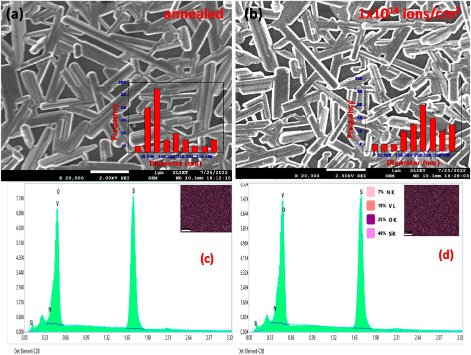
FIGURE 5. FE-SEM images and particle size distribution of V2O5 thin films on silicon substrate: (A) pristine; (B) after irradiation with N+ at 1 × 10¹⁴ ions/cm2; (C) EDS spectra of pristine; (D) EDS spectra of V2O5 thin films at 1 × 10¹⁴ ions/cm2 fluence.
The formation of smaller crystallites on the V2O5:Gl and nanorods on V2O5:Si matrix could be understood through the thermodynamics that occur at the interface. Thermal conductivity might be used to explain the observed variation in V2O5 crystallite shapes on different substrates. Glass has a thermal conductivity of 1 W/m.K, sapphire 35.8 W/(m)K, and silicon 148 W/(m)K (Santos et al., 2013). Therefore, compared to the sapphire and glass substrates, silicon exhibits better heat dissipation. In the case of V2O5:Si, when two particles integrate at an elevated temperature during annealing at the interface, the density of the bigger particles increases as a result of the nucleation of shorter-sized particles to lower the surface energy under a thermodynamic driving force. The different sticking coefficients and strains of V2O5 at the interface also depend on the amorphous and crystalline nature of the substrate. Ahmad et al. (Khan et al., 2015) have also modelled the crystallization of V2O5 thin films on different substrates. A mismatch in the lattice parameters of the deposited film and the substrate strongly influences the nucleation growth of particles due to a change in Gibbs free energy (Kwok et al., 1998; Yang and Liu, 2000; Santos et al., 2013). A correlation between the diffusion coefficient D and temperature T is stated as follows (Kittel, 1968):
where Ed is the activation energy for diffusion at temperature T and Do is a temperature-independent quantity that is material- and deposit-specific. Accordingly, the substrate’s material, temperature, and contact angle with the liquid embryo all play a role in the nucleation rate. Nucleation of V2O5 differs amongst substrates, even when deposited and annealed at the same temperature. Since the annealing conditions were the same for all substrates, the contact angle of V2O5 defines the adhesive force of nuclei with the substrate (Neumann A, 1979).
UV-vis study
The UV-vis absorption spectrum of pristine and ion-implanted V2O5 samples grown on glass substrates is shown in Figure 6A. As is evident, the absorption of the pristine sample is lowest and gradually increases after ion implantation in the visible range. However, the absorption curve is similar, and no additional peaks are formed. It has been observed that the ion implantation causes surface and bulk destruction through V and O vacancies, which translates into interstitial, substitutional, or vacancy defects within the material (Negreira and Wilcox, 2011; Jovanovic et al., 2018). This leads to the creation of defective energy states within the bandgap of V2O5, causing an increase in absorption. The values of band gap (Eg) were calculated by linearly extrapolating the Tauc plots [(αhν)2 vs hv] and are summarized in Table 1. When examining direct transition against indirect transition at the same band gap, it becomes immediately apparent that direct transition is more dominant and a better linear fit. Since there is no linear regime in (αhν)1/2 vs. hv, the indirect transition is less likely to happen. This shows that the V2O5 sample depicts a direct band transition with the highest value of band gap (Eg = 2.49 eV), which decreases to 2.05 eV at an ion fluence of 1×10¹⁴.
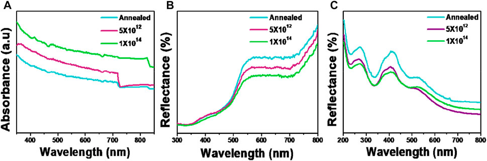
FIGURE 6. (A) Absorbance spectrum of pristine and N+ implanted samples on glass substrate. (B,C) Reflectance spectra of pristine and N+ implanted samples on sapphire and silicon substrates.
The diffuse reflectance spectra of V2O5 samples grown on sapphire substrates are shown in Figure 6B. The reflectance decreases with an increase in the ion fluence above 500 nm and is almost the same for all samples below 500 nm. The absorption band edge is approximately >500 nm for all samples, corresponding to an energy band of >2.48 eV. The optical Eg of the samples calculated using the Kubelka-Munk (KM) function is tabulated in Table 1. The KM function is given by
where R∞ = reflectance of the sample, α = absorption coefficient, and S = scattering coefficient. To calculate the bandgap, the KM function is plotted as a function of energy, hν, and the straight-line region is extrapolated. The bandgap comes out in the range of 2.51–2.69 eV, which agrees with the values reported in the literature. The decrease in Eg with ion fluence follows the same trend as that of the samples grown on glass substrates. The slight difference in the values of Eg for glass and sapphire samples can be explained by the difference in the phases that may induce growth-related stress.
Figure 6C shows the diffuse reflectance spectra of V2O5 films grown on silicon substrates. In this case, a clear difference in reflectance can be observed due to the presence of interference fringes, indicating a highly homogeneous film (Tiagarajan and Ganesan, 2015). Such a pattern has been reported in the literature for metal oxide films grown on silicon substrates (Venkatesan et al., 2013; Abazari et al., 2014). The N-implantation reduces the reflectance, which may be attributed to the creation of more scattering centres and grain boundaries due to N ions (Guo et al., 2021).
Electrical measurements
Current-voltage (I-V) measurements of V2O5:Gl, V2O5:Sp, and V2O5:Si are shown in Figures 7A–C, respectively. Silver (Ag) contacts are carved on glass and sapphire to make the I-V measurements. When the plots are linearly fitted, the slope gives the conductance (G) values. It was observed that the conductance values are lower in the case of V2O5:Gl (∼10−10 S) whereas there is a higher order of ∼10−9 S for V2O5:Sp, respectively. As the glass substrate is an insulator, the I-V characteristics purely come from the V2O5 film of a semiconducting nature (band gap range: 2.29–2.05 eV) which has been observed in UV measurement. A smaller conductance for V2O5:Gl is also expected due to the fewer conducting paths for low packed and scattered crystallite structures of V2O5, as observed in the FESEM study. According to Ibrahim (2022), electrical conductivity generally behaves similarly across all glass compositions and to decrease with increasing phosphate concentration. Burdyukh et al. (2018) found that W-metal implantation has a significant impact on the switching structures’ I-V curves. In the present study, conductance values show a gradually decreasing trend with increasing fluence of the N+ beam, as shown in Table 3. In the case of V2O5:Sp and V2O5:Si, the higher order of conductance is due to highly dense and long-range-ordered closely-packed nanorods. A similar trend in decreasing conductance has been observed for V2O5:Sp and V2O5:Si. In Figure 7C, V2O5:Si shows non-ohmic characteristics due to metal-semiconductor (Ag-Si) Schottky contacts. The V2O5 thin film as an interface layer between a Ag/p-Si diode exhibits good rectifying behaviour and enhanced diode characteristics.
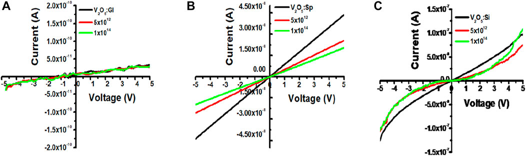
FIGURE 7. I-V characteristics of V2O5 thin films of (A) V2O5:Gl, (B) V2O5:Sp, and (C) V2O5:Si.
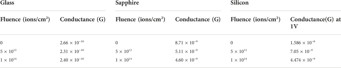
TABLE 3. Conductance values calculated from I-V graphs for each substrate, pristine, and after ion implantation.
For all substrates, conductance is found to decrease when these films are treated with higher fluence values. The electrical conductance of a substance is dependent on both the concentration and mobility of charge carriers. Generally, grain boundaries and trapping/scattering centres prevent the charge carriers from participating in the conduction mechanism. Grain barriers do not affect conductivity when the grain size is bigger than the mean free path of conducting electrons. Without grain-boundary scattering, electrons can travel through many grains before being deflected by phonons since optical and electrical behaviour is coupled. From the UV study, a decrease in band-gap of V2O5 thin films with N+ implantation fluence for all V2O5:Gl, V2O5:Sp, and V2O5:Si is expected to favour the higher conductance. The formation of defects and vanadium/oxygen vacancies under ion implantation increases the trapping/scattering of electron flow and dominates the carrier concentration in decreasing the conductance. To understand this behaviour, the ion implantation range, sputtering yield, depth distribution, and concentration of V and O vacancies are estimated from SRIM-TRIM 2008, as shown in Figures 8A–D.
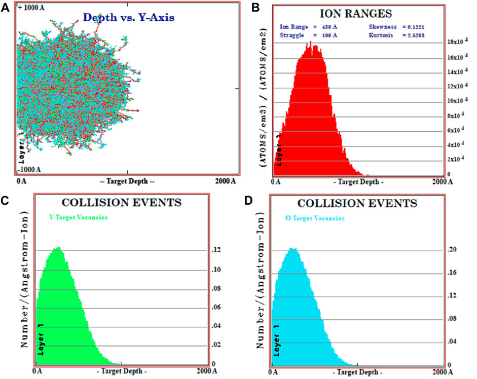
FIGURE 8. (A) Statistical distribution of 16 keV N+ ion implantation inside the V2O5 layer; (B) ion range parameter. Ion irradiation induced V and O vacancies in (C,D), respectively.
From Figures 8A and B, the estimated value of the 16 keV N+ ion-implantation damage range is found to be 104 nm inside the V2O5 layer. This N+ implantation also generates the sputtering of the target. The sputtering process is the removal of atoms from the target’s near surface. An atom may be sputtered when a cascade provides it with energy greater than its surface binding energy. When an atom crosses the surface’s plane, its energy normal to the surface must still be higher than the surface binding energy for it to sputter. A “sputtering yield,” which is defined as the average number of sputtered target atoms per incident ion, is used to characterise the sputtering of a surface. There is a distinct sputtering yield for each element if the target is composed of several components. In the present study, estimated values of sputtering yields are found to be 0.25 and 0.86 atoms/ion for V and O, respectively, for 16 keV N+. This higher sputtering of O generates higher vacancies of O in comparison to V up to the depth of N+ implantation, as observed in Figures 8C and D. The oxygen vacancies cascade the breaking of V=O and V-O-V bonds, as observed in the decreased intensities of peaks in XRD and FTIR studies. Hence, these broken bonds provide a large number of trapping and/or scattering centres to the flow of electrons/holes and result in a decrease in the conductance of V2O5 with an increase in ion fluence for all V2O5:Gl, V2O5:Sp, and V2O5:Si matrices. The decrease in conductance was attributed to an increase in trapping/scattering centres due to defect formation under ion implantation overshadowing the narrowing of the band gap.
Schematic modelling of the observed decrease in optical bandgap and electrical conduction of V2O5 thin film for the 16 keV N+ is presented in Figures 9A–D. In Figure 9A, the V2O5 orthorhombic structure has been presented before the N+ ion implantation. Ignoring the defects during thermal growth, the charge carriers are less hindered due to the well-crystallised nature of V2O5 and have the higher vector component of Ie along the applied electric field direction. A corresponding band structure has been presented in Figure 9C, where electron transitions can occur at the edges of the valance band (VB) to the conduction band (CB). Subsequent irradiation using N+ can induce the prominent O vacancies inside V2O5 under preferential sputtering, as observed from SRIM-TRIM and substitution of N, as shown in Figure 9B. Vanadyl oxygen O(1), bridging oxygen O(2), and triply coordinated oxygen O(3) have formation energies of 3.230 eV, 3.489 eV, and 4.464 eV, respectively (Ma et al., 2013). It has been reported that O(1) is the easiest oxygen vacancy and O(3) is the hardest to form, which is qualitatively observed in earlier research reports (Negreira and Wilcox, 2011; Nawaz1 et al., 2019). It is widely reported that enhancing the concentration of oxygen vacancies leads to a reduction in band gap, boosting ZnO’s ability to absorb visible light (Junpeng Wang et al., 2012). Thus, the presence of O vacancies can generate the shallow donor region above the valance band (Figure 9D). Hence, the observed reduction in optical band gap with N+ ion irradiation fluence is due to increased O vacancies. Furthermore, the scattering and trapping of charge carriers (e, h) through O vacancies and N substitution also lowers the Ie component along the field direction. In addition, the O vacancies generate the localized perturbing states in reticular defects, especially at the grain boundaries of semiconductors due to the presence of dangling bonds. The use of high-quality monocrystals helps mitigate their impact. The adoption of polycrystalline semiconductors is motivated by cost considerations, making it crucial to comprehend electrical grain boundary behaviour. However, because of constraints on the spatial resolution and sensitivity of electrical measurements, experimental investigations on the effect of grain boundary features such as the type, orientation, phase, and curvature on conductance are not explicitly measurable here. Nonetheless, the present study has been able to correlate the observed decrease in conductance with bandgap and oxygen vacancy, at least qualitatively. Hence, observation of the simultaneous reduction in the band gap, as well as electrical conductance, is very important for V2O5 thin films in various optoelectronic applications.
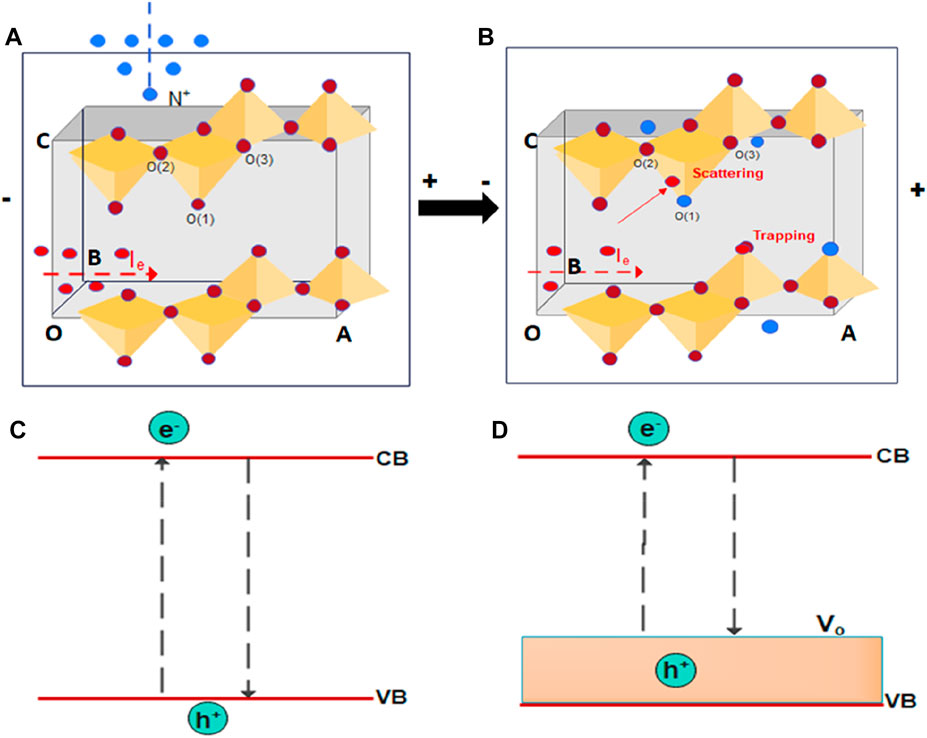
FIGURE 9. (A,B) shows the schematic representation of the mechanism of degradation of crystallinity, electrical conductance, and (C,D) shows the change in optical band gap of V2O5 before and after ion implantation respectively.
Summary
The structural, morphological, compositional, and electrical features of vanadium pentoxide (V2O5) thin films prepared on various substrates are examined regarding the influence of nitrogen (N+) ion implantation. On all substrates (sapphire, glass, and silicon), the mixed orthorhombic and tetragonal phases of V2O5 are seen in XRD analyses. Variations in the size of V2O5 crystallite forming on different substrates may be due to thermal conductivity. Silicon dissipates heat better than sapphire and glass. In V2O5:Si, when two particles integrate at a higher temperature during annealing at the interface, the bigger particles’ density rises due to the nucleation of shorter particles to reduce the surface energy under a thermodynamic driving force. A decrease in the crystalline characteristic of V2O5 under N+ implantation is observed on all V2O5:Gl, V2O5:Si, and V2O5:Sp matrices due to the generation of ion implantation-induced defects. The ion implantation-induced strain is responsible for the change in crystallite size, which may be described by a deformation that occurs in the β-phase of V2O5 thin films. Glass and sapphire both encourage the formation of individual crystallites, but V2O5:Si results in the synthesis of nanorods of a consistent size throughout the material. After the N+ implantation, it was observed that the electrical conductance of thin films and the band gap had reduced. This was caused by an increase in the number of oxygen vacancies and electron scattering and trapping centres. The present study finds advantages in a simultaneous decrease in the optical band-gap and conductance of V2O5 thin films, which can potentially be used in optoelectronic applications.
Data availability statement
The raw data supporting the conclusion of this article will be made available by the authors, without undue reservation.
Author contributions
BP, PJ, and TK planned the experiment and also performed the characterizations. RK and PK have conducted the ion implantation on the samples. AK, VS, and JJ have performed the UV-vis and electrical analysis.
Acknowledgments
The authors would like to express deepest appreciation and gratitude to Dr. Vinay Kumar, CUJ, for his unwavering support, and to RK, IUAC, New Delhi, for allowing the use of the table top accelerator. The Satish Dhawan Space centre facility, CUJ, is acknowledged for its characterization facilities.
Conflict of interest
The authors declare that the research was conducted in the absence of any commercial or financial relationships that could be construed as a potential conflict of interest.
Publisher’s note
All claims expressed in this article are solely those of the authors and do not necessarily represent those of their affiliated organizations, or those of the publisher, the editors, and the reviewers. Any product that may be evaluated in this article, or claim that may be made by its manufacturer, is not guaranteed or endorsed by the publisher.
References
Abazari, R., Sanati, S., and Saghatforoush, L. A. (2014). Non-aggregated divanadium pentoxide nanoparticles: A one-step facile synthesis. Morphological, structural, compositional, optical properties and photocatalytic activities. Chem. Eng. J. 236, 82–90. doi:10.1016/j.cej.2013.09.056
Arbab, E. A. A., and Mola, G. T. (2016). V2O5 thin film deposition for application in organic solar cells. Appl. Phys. A 122 (8), 405. doi:10.1007/s00339-016-9966-1
Beke, S. (2011). A review of the growth of V2O5 films from 1885 to 2010. Thin Solid Films 519 (6), 1761–1771. doi:10.1016/j.tsf.2010.11.001
Cocciantelli, J. M., Gravereau, P., Doumerc, J. P., Pouchard, M., and Hagenmuller, P. (1991). On the preparation and characterization of a new polymorph of V2O5. J. Solid State Chem. 93, 497–502. doi:10.1016/0022-4596(91)90323-a
Couster, F., Passerini, S., and Smyrl, W. H. (1997). Dip-coated silver-doped V2O5 xerogels as host materials for lithium intercalation. Solid State Ionics 100 (3–4), 247–258. doi:10.1016/s0167-2738(97)00354-8
Coustier, F., Jarero, G., Passerini, S., and Smyrl, W. H. (1999). Performance of copper-doped V2O5 xerogel in coin cell assembly. J. Power Sources 83 (1–2), 9–14. doi:10.1016/s0378-7753(99)00243-8
El Desoky, M. M., Al-Assiri, M. S., and Bahgat, A. A. (2014). Study of structural. J. Phys. Chem. Solids 75, 992–997. doi:10.1016/j.jpcs.2014.04.003
Enjalbert, J. G. R., and Galy, J. (1986). A refinement of the structure of V2O5. Acta Crystallogr. C 42, 1467–1469. doi:10.1107/s0108270186091825
Eric Kumi-Barimah, G. J., Anagnostou, D. E., and Jose, G. (2020). Phase changeable vanadium dioxide (VO2) thin films grown from vanadium pentoxide (V2O5) using femtosecond pulsed laser deposition. AIP Adv. 10, 065225. doi:10.1063/5.0010157
Filonenko, V. P., Sundberg, M., Werner, P.-E., and Zibrov, I. P. (2004). Structure of a high-pressure phase of vanadium pentoxide, beta-V2O5. Acta Crystallogr. B 60, 375–381. doi:10.1107/s0108768104012881
Guo, D., Senthil Kumar, N., Chang, J. H., Ho, M-S., Balraj, B., Chandrasekar, S., et al. (2021). Impact of Zn2+ doping on the structural, morphological and photodiode properties of V2O5 nanorods. J. Inorg. Organomet. Polym. Mat. 31, 1066–1078. doi:10.1007/s10904-020-01751-y
Hwang, H. S., Oh, S. H., Kim, H. S., Cho, W. I., Cho, B. W., and Lee, D. Y. (2004). Characterization of Ag-doped vanadium oxide (AgxV2O5) thin film for cathode of thin film battery. Electrochimica Acta 50 (2–3), 485–489. doi:10.1016/j.electacta.2004.04.050
Ibrahim, F. A. (2022). Electrical conductivity enhancement of V2O5-P2O5-Bi2O3 glasses by nanocrystallization. J. Electron. Mat. 51, 621–625. doi:10.1007/s11664-021-09308-6
Jin, G. S., Chen, W., Zhu, Q., Yang, Y., Volkov, V. L., and Zakharova, G. (2009). Structural and electrochromic properties of molybdenum doped vanadium pentoxide thin films by sol–gel and hydrothermal synthesis. Thin Solid Films 517 (6), 2023–2028. doi:10.1016/j.tsf.2008.10.001
Jovanovic, A., Dobrota, A., Rafailovic, L. D., Mentus, S. V., Pasti, I. A., Johansson, B., et al. (2018). Structural and electronic properties of V2O5 and their tuning by doping with 3d elements – modelling using the DFT+U method and dispersion correction. Phys. Chem. Chem. Phys. 20, 13934–13943. doi:10.1039/c8cp00992a
Junpeng Wang, Y. D., Wang, Z., Huang, B., Ma, Y., Liu, Y., Qin, X., et al. (2012). Oxygen vacancy induced band-gap narrowing and enhanced visible light photocatalytic activity of ZnO. ACS Appl. Mat. Interfaces 4 (8), 4024–4030. doi:10.1021/am300835p
Kenny, D. H. W. N., Kannewurf, C. R., and Whitmore, D. (1966). Optical absorption coefficients of vanadium pentoxide single crystals. J. Phys. Chem. Solids 27, 1237–1246. doi:10.1016/0022-3697(66)90007-2
Khan, G. R., Bilal Ahmad Bhat, K. A., and Asokan, K. (2015). Role of substrate effects on the morphological, structural, electrical and thermoelectrical properties of V2O5 thin films. RSC Adv. 5, 52602–52611. doi:10.1039/c5ra07542d
Kim, Y. S., and Ahn, H. J. (2006). Effect of oxygen vacancy on Li-ion diffusion in a V2O5 cathode: A first-principles study. Solid StateIon 177, 1323.
Kumar, N. B. S., Qadir, A., Maury, F., and Bahlawane, N. (2017). Visible thermochromism in vanadium pentoxide coatings. ACS Appl. Mat. Interfaces 9, 21447–21456. doi:10.1021/acsami.7b04484
Kwok, D. Y., Lam, C. N. C., Li, A., Leung, A., Wu, R., Mok, E., et al. (1998). Measuring and interpreting contact angles: A complex issue. Colloids Surfaces A Physicochem. Eng. Aspects 142 (2), 219–235. doi:10.1016/s0927-7757(98)00354-9
Legrouri, A., Baird, T., and Fryer, J. R. (1993). Electron optical studies of fresh and reduced vanadium pentoxide-supported rhodium catalysts. J. Catal. 140 (1), 173–183. doi:10.1006/jcat.1993.1076
Li, G., Yao, J., Uchaker, E., Zhang, M., Tian, J., Liu, X., et al. (2013). Sn-doped V2O5 film with enhanced lithium-ion storage performance. J. Phys. Chem. C 117 (45), 23507–23514. doi:10.1021/jp406927m
Liu, Y., Cao, G., Li, J. G., Zhang, Q. F., Zhou, N., and Uchaker, E. (2011). Porous nanostructured V2O5 film electrode with excellent Li-ion intercalation properties. Electrochem. Commun. 13, 1276–1279. doi:10.1016/j.elecom.2011.08.024
Lu, Q. L. J., Hu, M., Tian, Y., Guo, C., Wang, C., Guo, S., et al. (2012). Fast visible light photoelectric switch based on ultralong single crystalline V_2O_5 nanobelt. Opt. Express 20, 6974–6979. doi:10.1364/oe.20.006974
Ma, W. Y., Zhou, B., Wang, J. F., Zhang, X. D., and Jiang, Z. Y. (2013). Effect of oxygen vacancy on Li-ion diffusion in a V2O5 cathode: A first-principles study. J. Phys. D. Appl. Phys. 46 (10), 105306. doi:10.1088/0022-3727/46/10/105306
Majumdar, S. K. B., Mandal, M., and Bhattacharya, S. K. (2019). V2O5 and its carbon-based nanocomposites for supercapacitor applications. ChemElectroChem 66, 16231623–16481648. doi:10.1002/celc.201801761
Metin, A., Gasal, B., Kiskan, B., Yusuf, Y., and Toppare, L. (2008). Enhancing electrochromic properties of polypyrrole by silsesquioxane nanocages. Polymer 49 (9), 2202–2210. doi:10.1016/j.polymer.2008.03.023
Nawaz1, T., Waqar, A. A. S., Ahmad, I., and Shah, W. H. (2019). Cu ion beam induced effects and phase study of vanadium oxide thin films. Mat. Res. Express 6, 075707. doi:10.1088/2053-1591/ab1702
Negreira, A. S., and Wilcox, J. (2011). Surface reactivity ofV2O5(001): Effects of vacancies, protonation, hydroxylation, and chlorination. Phys. Rev. B 83, 045423. doi:10.1103/physrevb.83.045423
Neumann A, G. R. (1979). Contact angles and the surface free energy of solids. Surf. Colloid Sci. II, 1–29. doi:10.1007/978-1-4615-7969-4_1
PrzeVniak-Welenc, M., AapiNski, M., and Lewandowski, T. (2015). The influence of thermal conditions on V2O5 nanostructures prepared by sol-gel method. J. Nanomater 2015. 418024. doi:10.1155/2015/418024
Rao, M. C. (2013). Vanadium pentoxide cathode material for fabrication of all solid state lithium-ion batteries -a case study. Res. J. Recent Sci. 2, 67–73.
RezaBenama, M. M.-M., Bagheri-Mohagheghi, M. M., and Benam, M. R. (2015). Study of structural and optical properties of nanostructured V2O5 thin films doped with fluorine. Mater. Sci. Semicond. Process. 31, 693–699. doi:10.1016/j.mssp.2014.12.049
Santos, R., Loureiro, J., Nogueira, A., Elangovan, E., Pinto, J. V., Veiga, J. P., et al. (2013). Thermoelectric properties of V2O5 thin films deposited by thermal evaporation. Appl. Surf. Sci. 282, 590–594. doi:10.1016/j.apsusc.2013.06.016
Sergey Burdyukh, A. P., Berezina, O., and Pergament, A. (2018). Modification of the properties of vanadium oxide thin films by plasma-immersion ion implantation. Adv. Condens. Matter Phys. 2018, 1–14. doi:10.1155/2018/9789370
Smallman, R. E., and Williamson, G. K. (1956). Dislocation densities in some annealed and cold-worked metals from measurements on the X-ray debye-scherrer spectrum. Philos. Mag. Abingdon (Abingdon) 1 (1), 34–46.
Suresh, R., Giribabu, K., Manigandan, R., Munusamy, S., Praveen Kumar, S., Stephen, V. N. A., et al. (2014). Doping of Co into V2O5 nanoparticles enhances photodegradation of methylene blue. J. Alloys Compd. 598, 151–160. doi:10.1016/j.jallcom.2014.02.041
Tiagarajan, S., Thaiyan, M., and Ganesan, R. (2015). Physical property exploration of highly oriented V2O5 thin films prepared by electron beam evaporation. New J. Chem. 39 (12), 9471–9479. doi:10.1039/c5nj01582k
Venkatesan, A., Krishna Chandar, N., Arjunan, S., Marimuthu, K. N., Mohan Kumar, R., and Jayavel, R. (2013). Structural, morphological and optical properties of highly monodispersed PEG capped V2O5 nanoparticles synthesized through a nonaqueous route. Mater. Lett. 91, 228–231. doi:10.1016/j.matlet.2012.09.117
Volkov, Y. G. Z. V. L., Golovkin, B. G., and Fedyukov, A. S. (1988). Synthesis and properties of β-V2O5. Inorg. Mat. 24, 1836–1840.
Wei, Y., Zhou, J., Zheng, J., and Xu, C. (2015). Improved stability of electrochromic devices using Ti-doped V2O5 film. Electrochimica Acta 166, 277–284. doi:10.1016/j.electacta.2015.03.087
Yang, B. X., and Liu, G. W. (2000). Nucleation thermodynamics of quantum-dot formation in Vgroove structures. Phys. Rev. B 61 (7), 4500–4502. doi:10.1103/physrevb.61.4500
Yu, Q. Y. H., Rui, X., Tan, H., Chen, J., Huang, X., Xu, C., et al. (2013). Cu doped V2O5 flowers as cathode material for high-performance lithium ion batteries. Nanoscale 5, 4937–4943. doi:10.1039/c3nr00548h
Zhan, J. S., Chen, G., Liu, D., Li, A., Wang, C., and Wei, Y. (2009). Effects of Cr doping on the structural and electrochemical properties of V2O5. J. Alloys Compd. 479 (1–2), 652–656. doi:10.1016/j.jallcom.2009.01.023
Keywords: ion implantation, crystallite, microscopy, conductance, nanorod
Citation: Priya B, Jasrotia P, Kumar A, Singh V, Jire L. Hmar J, Kumar R, Kulriya PK and Kumar T (2022) Structural, optical, and electrical properties of V2O5 thin films: Nitrogen implantation and the role of different substrates. Front. Mater. 9:1049189. doi: 10.3389/fmats.2022.1049189
Received: 20 September 2022; Accepted: 15 November 2022;
Published: 15 December 2022.
Edited by:
Pratap K. Sahoo, National Institute of Science Education and Research (NISER), IndiaReviewed by:
Kamakhya Prakash Misra, Manipal University Jaipur, IndiaVali Dalouji, Malayer University, Iran
Copyright © 2022 Priya, Jasrotia, Kumar, Singh, Jire L. Hmar, Kumar, Kulriya and Kumar. This is an open-access article distributed under the terms of the Creative Commons Attribution License (CC BY). The use, distribution or reproduction in other forums is permitted, provided the original author(s) and the copyright owner(s) are credited and that the original publication in this journal is cited, in accordance with accepted academic practice. No use, distribution or reproduction is permitted which does not comply with these terms.
*Correspondence: Tanuj Kumar, dGFudWoubnNtQGN1amFtbXUuYWMuaW4=