 Wang Tian
 Dong-liang Zhang
 Xian-tong Zheng*
- Key Laboratory of the Ministry of Education for Optoelectronic Measurement Technology and Instrument, Beijing Information Science and Technology University, Beijing, China
High material quality is the foundation for the excellent performance of quantum cascade lasers. This paper investigates the growth conditions for InGaAs/InAlAs/InP superlattices combined solid-source molecular beam epitaxy with metal-organic chemical vapor deposition. Based on the optimization of growth conditions of InGaAs buffer epilayers, the effects of the growth temperature, interruption time, and V/III flux ratio on the quality of InGaAs/InAlAs/InP superlattices were systematically investigated. High-resolution x-ray diffraction and atomic force microscopy prove that this optimized InP-based superlattice has excellent periodicity and sharp interfaces.
1 Introduction
Quantum cascade lasers (QCLs) are semiconductor laser sources based on intersubband transitions (Gmachl, Capasso, Sivco and Cho, 2001). After the first QCL was invented in 1994, the first Distributed feedback (DFB) quantum cascade laser capable of room temperature single-mode operation was demonstrated in 1997, and in 2002, the first continuous room temperature operation of a QCL was achieved (Faist et al., 1994, pp.553–556; Faist et al., 1997, pp.2670–2,672; Beck et al., 2002, pp.301–305). QCL technology has realized practical application in some segmented fields, such as free-space optical communication, infrared directional countermeasures, and trace gas detection (Zhang and Sun, 2011; Giglio et al., 2020; Pang et al., 2020). Recently, high-power QCL devices are also attracting more interest than ever (Lu et al., 2020; Shcherbakova et al., 2021, pp.830–837; Vanier et al., 2022, pp.361–368). It will play an increasingly important role in future national defense and civil fields.
InGaAs/InAlAs/InP materials systems that can be grown by molecular beam epitaxy (MBE) or metal-organic chemical vapor deposition (MOCVD) are commonly used to construct QCL in mid-infrared wavelengths. These materials can be grown by solid-source molecular beam epitaxy (SSMBE), gas source molecular beam epitaxy (GsMBE), and MOCVD. However, InP is difficult to grow by SSMBE due to the limitations of solid-state phosphorus (P) source technology, and MOCVD is unsatisfactory in precise control of the low dimensional structure. GsMBE equipment is used for the high-power QCL (Lu et al., 2020) material growth by Northwestern University, but the equipment is too complex. The quality of the material is the basis for good device performance and reproducibility (Liu et al., 2001, pp.1831–1835). In particular, for complex ternary systems, the requirements for the precise control of its composition, layer thickness, and interface quality make the heterogeneous epitaxial growth of InP-based QCL structures very challenging (Moison et al., 1989). However, the current QCL literature focuses on the performance aspects of devices, with little work reported on strong material growth. Here, we demonstrate the growth details of an InP-based InGaAs/InAlAs superlattice structure for the QCL active region combined SSMBE with MOCVD technology, such as the growth temperature, interruption time, and optimal V/III flux ratio. The composition and thickness of heterostructures and crystal quality were determined by High-resolution x-ray diffraction (HRXRD) and atomic force microscopy (AFM).
Furthermore, for the growth of the QCL full structure, obtaining the growth conditions of the strain-compensated component of the InGaAs/InAlAs/InP material system is necessary. The in this component condition exceeds the critical thickness and relaxes after a few tens of nanometers, so it is not possible to determine the indium component and growth rate by the growth of thick layers (Gutowski et al., 2017, pp.22–29); superlattice test structures can only achieve the calibration of this process. However, the results of diffraction simulations of simple superlattice structures of ternary alloys with two unknown components are not unique; such a double superlattice structure in the same growth cycle can eliminate one unknown parameter, which is a suitable solution to adjust the components and growth rate. This paper may fill the gap in the literature by discussing essential factors that influence the growth process and lay the foundation for the growth of a perfect QCL full structure based on MBE combined with MOCVD.
2 Materials and methods
All the samples are grown on a Komponenten Octoplus 400 multi-chamber 3-inch wafer ultrahigh vacuum MBE system, which is equipped with arsenic (As) valved cracker cells and dual-filament thermal evaporation cells of indium (In) and gallium (Ga), cold-lip filament effusion cell for aluminium (Al). Because of the lack of P source in MBE, 20 nm In0.53Ga0.47As buffer was first grown on the n-doped InP (100) substrate by MOCVD before being transferred to the MBE chamber, then the substrate was deoxidized at 500°C for 10 min, while the As valve is opened when the substrate temperature exceeds 300°C during the deoxidization process. This paper investigated different growth conditions for InGaAs buffer epilayers near lattice-matched to InP substrate. After searching the target composition’s epitaxial layers growth parameters, the optimization of growth temperatures, interruption time, and optimal V/III flux ratio for InGaAs/InAlAs/InP superlattices was investigated. HRXRD and AFM were used to characterize grown samples.
Firstly, the buffer epilayer is critical to the quality of superlattice growth, and individual InGaAs epilayer samples were grown on InP (100) oriented semi-insulating substrates. Previously, 1 µm InP doped Si with 2 cm × 1016 cm−3 and 20 nm undoped Ga0.47In0.53As buffer layer were grown on a 2-inch n-doped InP substrate using MOCVD. The optimum growth conditions were investigated by growing test samples at different temperatures and As flux.
Once the compositions of the monolayer material have been obtained, the subsequent work will focus on optimizing the superlattice based on the above monolayer epitaxial conditions. Generally, the two main growth parameters determining growth mode and layer quality are the V/III ratio and substrate temperature. The deposition parameters need to be refined to facilitate the growth of nanofilms. Due to the burst effect that occurs when the cells are switched frequently for a short time (Gutowski et al., 2017, pp.22–29), the composition and growth rate of the thin layers can be different from the parameters of the bulk layers grown under the same epitaxial conditions. Lots of work had to be done to adjust the epitaxial BEP and growth rate to achieve the target structure, so 60 periods of InGaAs/InAlAs test superlattices were grown at different conditions. Based on the previous process, the final optimized structure of double InGaAs/InAlAs/InP superlattices is obtained, and its simulated diffraction is plotted with the experimental data.
3 Results and discussion
3.1 Optimization of InGaAs buffer epilayer
The development of the growth process started with the crystallization of lattice-matched In0.53Ga0.47As monolayers. The deposition process is carried out referring to the investigation of Liu et al. (2009), pp. 527–532, with the necessary adjustments taking into account the differences between the epitaxial systems. Generally, InGaAs grow better at low substrate temperatures and high V/III ratios, while InAlAs tend to grow better at elevated substrate temperatures and low V/III ratios (Monastyrskyi et al., 2013, pp.614–617; Gutowski et al., 2019). For the subsequent growth of the superlattice, the same substrate temperature and As beam flux was needed for both material’s epitaxy.
Figure 1 illustrates that the in beam equivalent pressure (BEP) was fixed, and the Ga/In and Al/In flux ratios were adjusted to achieve the desired composition. The optimal Ga/In flux ratio is 0.68 for the near lattice-matched composition of InGaAs.
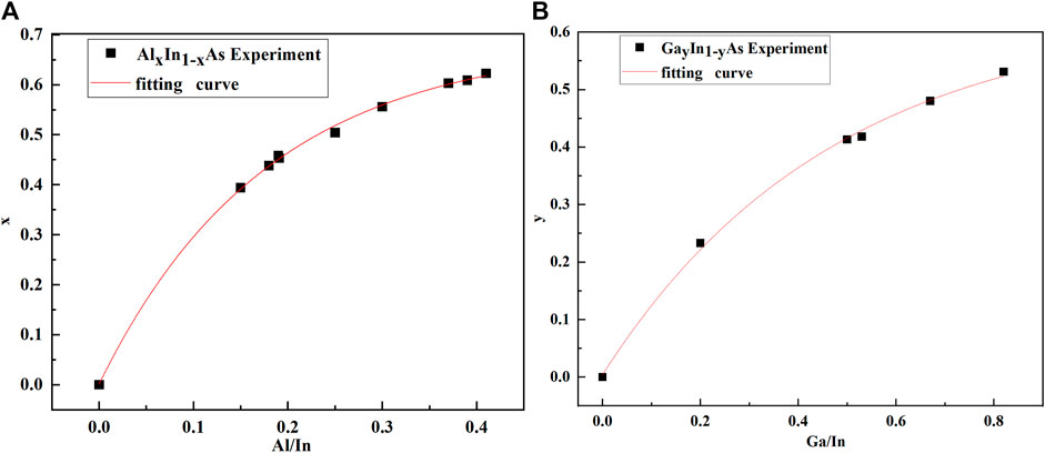
FIGURE 1. (A) Fitting curve of the Al compositions in AlxIn1-xAs to the Al/In flux ratios; (B) Fitting curve of the Ga compositions in GaxIn1-xAs to the Ga/In flux ratios.
Considering there is no possibility of changing growth conditions during superlattice growth, we have accepted a compromised solution to find the best conditions, i.e., the V/III ratio of InGaAs and InAlAs equal to 15.68 and 20.36, respectively, and the substrate temperature is 420°C–430°C.
As shown in Figure 2, HRXRD was used to determine the compositions and thickness of InGaAs epilayers, narrow peaks, interferometric fringes, and small RMS in Figure 2A, the appearance of interference fringes indicates good crystalline quality integrity and uniform thickness of the epitaxial layer the FWHM value of the substrate is at 13.1 arcseconds, while the InGa0.463As epitaxial layer is at 49.2 arcseconds, indicating the excellent quality of the materials. The AFM image of Figure 2B represented that the surface roughness of the substrate was 0.2 nm over a 5 μm × 5 µm square area, and it showed a step-flow growth mode, whose step edges are smooth, and kinks occur. The abundant steps indicate low defectivity in InGaAs layers with atomic flatness.
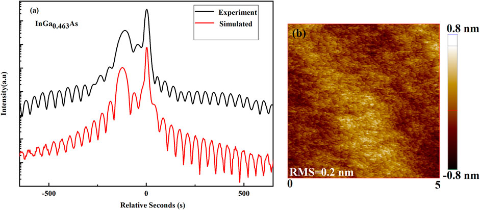
FIGURE 2. (A) Typical double crystal X-ray diffraction results. Simulated diffraction plotted along with experimental data shows the excellent epitaxial control and material quality; (B) AFM (5 μm × 5 µm square area) images of InGa0.463As buffer combined MBE with MOCVD.
3.2 Optimization of InGaAs/InAlAs/InP superlattice
3.2.1 The effect of growth temperature on the superlattice quality
Generally, the substrate temperature cannot be too high for InGaAs growth, while InAlAs tend to grow better at elevated substrate temperatures. We accepted a compromise solution as there was no possibility to change the growth conditions during the growth of the superlattice as well as the QCL core region. Therefore, 60 periods of 2 nm-InGa0.463As/2 nm-InAl0.489As test superlattices were grown at different temperatures.
It can be seen from Figures 3A–H that the bottom of the nanopore is lower than the surface of the superlattice, which indicates that the nanopore is formed by removing materials from the surface. A lot of black nanoholes appeared on the sample’s surface from 440°C. With the increase in temperature, the density of the nanoholes also increased, and ring-like-shaped walls surrounding the openings are visible at 480°C, presumably due to local droplet etching (LDE) that was demonstrated for drilling of nanoholes into InGaAs or InAlAs surfaces with Ga droplets as the etchant. The Ga deposition results in forming low-density Ga droplets in Volmer-Weber growth mode. At temperatures above 420°C, the substrate was desorbed into the liquid droplet material, resulting in liquefaction of the substrate at the interface to the droplet, forming stochastic distribution nanoholes; the As diffusing out of the substrate crystallized in contact with the Ga droplet material above it to the growth of GaAs walls around the nanoholes (Sablon et al., 2008, pp.530–533; Heyn et al., 2009, pp.576–580). As Figure 3I illustrates, the difference in spacing between the XRD satellite peaks increases with higher temperature, which may be caused by the evaporation of elements from the Group III and Group V effusion cells, the deposition rate decreases, and the period thickness reduced (Wang et al., 2007). Relative low surface roughness at growth temperatures is 420°C. The XRD results of the samples from 420°C showed that the FWHM of the zero-level peaks were 41.2 s, 48.5 s, 40.4 s, and 49.6 s, respectively, as the temperature increased, indicating a close test result.
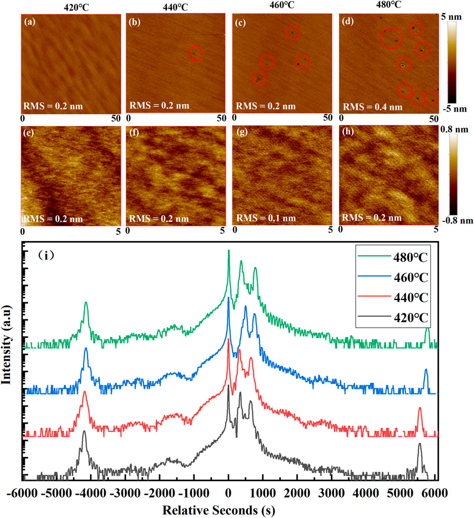
FIGURE 3. (A–H) AFM and (I) double crystal x-ray diffraction images of 60 periods of 2 nm-InGaAs/2 nm-InAlAs/InP superlattice in different growth temperature. The estimated root mean square (RMS) of surface roughness is demonstrated.
The surface of the AFM at 420°C appeared smoother without visible defects. Both analyses considering AFM and XRD showed that 420°C was the optimum temperature condition.
3.2.2 The effect of interruption time on the superlattice quality
After determining the growth temperature of 420°C, we investigated the effect of the interruption time, which means different stabilization times and BEP for the group III effusion cell during superlattice growth. 60 periods of 6 nm-InGa0.463As/2 nm-InAl0.489As test superlattices with varying interruption times were grown.
It can be observed that with increasing interruption time, the sample surface changes from openings defects to nanoholes defects with lower defect depth but much higher density combined with in Figure 4A–G. When the cell opened during the growth of the superlattice, large-sized nanoholes with openings were created on the surface of the sample due to the LDE of Ga droplets, after which the interruption time of the cell increased, the BEP of group III elements such as Ga, In and Al reduces, which leads to a less likely to form openings with As, smaller sized nanoholes were left on the Ga etched surface. A flat surface is obtained clearly at an interruption time of 2 s.
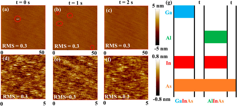
FIGURE 4. (A–F): AFM images of the surface of 60-periods 6 nm-InGa0.463As/2 nm-InAl0.489As/InP superlattices in different interruption times at Ts = 420°C (up: 50 μm × 50 µm scan area; down: 5 μm × 5 µm scan area), estimated root mean square (RMS) of surface roughness is demonstrated. (G) The shutter sequence of the superlattices growth.
3.2.3 The effect of V/III ratio on the superlattice quality
The V/III ratio represents the flux of as during the growth process, and a suitable V/III ratio can inhibit the desorption of In (Choi and Fonstad, 1994), which guarantees good surface growth quality. InAlAs grow better at a low V/III ratio, while InGaAs grow better at a high V/III ratio. 60 periods of 6 nm-InGaAs/2 nm-InAlAs test superlattices with different V/III ratios were grown. To study the effect of V/III ratios on superlattice growth under an overall stable flux, an identical and stable As flux is necessary, so changing the V/III ratio of InAlAs will also result in a change in the V/III ratio in InGaAs.
From the results of the AFM test in Figure 5, lots of nanoholes appeared on the surface of the sample at a V/III (InAlAs) ratio less than 20, Figure 5A–C indicated nanoholes density and surface roughness decreased significantly with As flux increasing, which lead to the suppression in strong perturbation of growth and surface decomposition, Figures 5D–F showed the nanoholes of up to about 8 nm appear on the surface. The preferred V/III (InAlAs) is equal to 20. Considering the above factors, the select growth parameters are a V/III ratio of 12.5, an interruption time of 2 s, and a substrate temperature of 420°C.
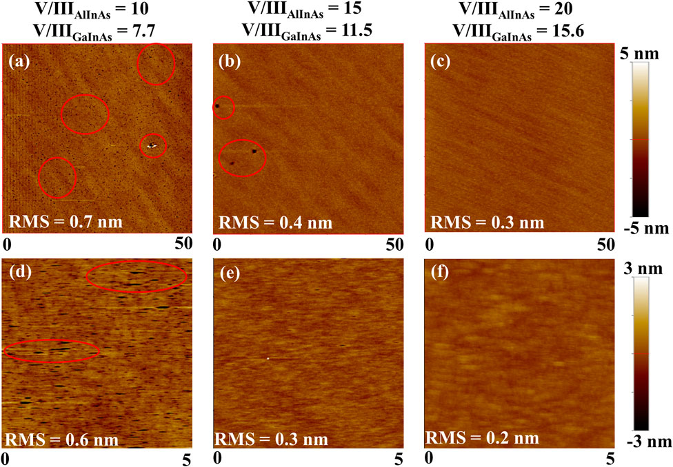
FIGURE 5. AFM image of the surface of 60-periods 6 nm-InGaAs/2 nm-InAlAs/InP superlattices in different V/III ratios at Ts = 420°C, t = 2s. The estimated root mean square (RMS) of surface roughness is demonstrated [(A–C): 50 μm × 50 μm scan area; (D–F): 5 μm × 5 μm scan area].
A stable beam flux is a key to obtaining the designed components and thickness. The BEP of the SSMBE cell could vary significantly over different time scales. The steady beam flux after 2 min is suitable for the growth of thick buffer layers, and the beam flux within 25 s is ideal for the growth of thin layers in double superlattices. Figure 6 shows the final optimal double InGaAs/InAlAs/InP superlattice structure. Simulated diffraction plotted along with experimental data shows the full width at half maxima (FWHM) of zero order peak is 61.2 s, and the fitted structure, which consists of 2.83 nm-InGa0.40As/2.36 nm-InAl0.59As superlattice with 50 repetitions followed by 1.82 nm-InGa0.40As/1.77 nm -InAl0.59As superlattice with 25 periods on InGa0.47As buffer. As the HRXRD and AFM test results are shown in Figure 6, narrow peaks, interferometric fringes, and small RMS indicate the excellent quality of the materials.
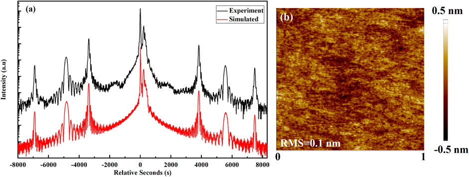
FIGURE 6. (A) Double crystal x-ray diffraction results for the final optimal double InAlAs/InGaAs/InP superlattice structure; (B) AFM (1 μm × 1 µm square area) image of final optimal double InAlAs/InGaAs/InP superlattice.
4 Conclusion
In this paper, the superlattice structure was optimized in terms of growth temperature, interruption time, and V/III ratio, and it was finally found that 2.83 nm-InGa0.40As/2.36 nm-InAl0.59As superlattice with 50 repetitions followed by 1.82 nm-InGa0.40As/1.77 nm-InAl0.59As superlattice with 25 periods on InGa0.47As buffer at 420°C obtains the best growth quality, corresponding to the V/III (GaInAs) = 15.68 and V/III (AlInAs) = 20.37 respectively. It was also found during the growth process that the similarity of the periodic thicknesses of GaInAs and AlInAs would lead to satellite front phase extinction in the HRXRD test results.
In summary, this paper has investigated the growth conditions of high-quality InGaAs/InAlAs/InP superlattice for QCL based on SSMBE combined with MOCVD. HRXRD and AFM characterization results show that our grown InP-based superlattices have fine periodic behavior, uniform layer thickness, and smooth interfaces. On this basis, the subsequent work will focus on the growth and optimization of the QCL active region complete structure based on the InGaAs/InAlAs/InP material system to provide a guarantee for the manufacture of the final QCL device.
Data availability statement
The original contributions presented in the study are included in the article/supplementary material, further inquiries can be directed to the corresponding authors.
Author contributions
Material growth and test analysis by WT, DZ, XZ, and RY, materials structure designed by YL, LL, and LZ.
Funding
This work was supported by the Beijing Scholars Program (74A2111113), Research Project of Beijing Education Committee (KM202111232019), National Natural Science Foundation of China (62105039) and Research Project of Beijing Information Science and Technology University (2022XJJ07).
Conflict of interest
The authors declare that the research was conducted in the absence of any commercial or financial relationships that could be construed as a potential conflict of interest.
Publisher’s note
All claims expressed in this article are solely those of the authors and do not necessarily represent those of their affiliated organizations, or those of the publisher, the editors and the reviewers. Any product that may be evaluated in this article, or claim that may be made by its manufacturer, is not guaranteed or endorsed by the publisher.
References
Beck, M., Hofstetter, D., Aellen, T., Faist, J., Oesterle, U., Ilegems, M., et al. (2002). Continuous wave operation of a mid-infrared semiconductor laser at room temperature. Science 295, 301–305. doi:10.1126/science.1066408
Choi, W. Y., and Fonstad, C. G. (1994). Growth optimization of molecular beam epitaxy grown InAlAs on InP. J. Vac. Sci. Technol. B 12, 1013. doi:10.1116/1.587117
Faist, J., Capasso, F., Sivco, D. L., Sirtori, C., Hutchinson, A. L., and Cho, A. Y. (1994). Quantum cascade laser. Science 264, 553–556. doi:10.1126/science.264.5158.553
Faist, J., Gmachl, C., Capasso, F., Sirtori, C., Sivco, D. L., Baillargeon, J. N., et al. (1997). Distributed feedback quantum cascade lasers. Appl. Phys. Lett. 70, 2670–2672. doi:10.1063/1.119208
Giglio, M., Zifarelli, A., Sampaolo, A., Menduni, G., Elefante, A., Blanchard, R., et al. (2020). Broadband detection of methane and nitrous oxide using a distributed-feedback quantum cascade laser array and quartz-enhanced photoacoustic sensing. Photoacoustics 17, 100159. doi:10.1016/j.pacs.2019.100159
Gmachl, C., Capasso, F., Sivco, D. L., and Cho, A. Y. (2001). Recent progress in quantum cascade lasers and applications. Rep. Prog. Phys. 64, 1533–1601. doi:10.1088/0034-4885/64/11/204
Gutowski, P., Sankowska, I., Karbownik, P., Pierścińska, D., Serebrennikova, O., Morawiec, M., et al. (2017). MBE growth of strain-compensated InGaAs/InAlAs/InP quantum cascade lasers. J. Cryst. Growth 466, 22–29. doi:10.1016/j.jcrysgro.2017.02.031
Gutowski, P., Sankowska, I., Slupinski, T., Pierscinska, D., Pierscinski, K., Kuzmicz, A., et al. (2019). Optimization of MBE growth conditions of In0.52Al0.48As waveguide layers for InGaAs/InAlAs/InP quantum cascade lasers. Mater. (Basel) 12, 1621. doi:10.3390/ma12101621
Heyn, C., Stemmann, A., Koppen, T., Strelow, C., Kipp, T., Grave, M., et al. (2009). Optical properties of GaAs quantum dots fabricated by filling of self-assembled nanoholes. Nanoscale Res. Lett. 5, 576–580. doi:10.1007/s11671-009-9507-3
Liu, F.-Q., Li, L., Wang, L.-J., Liu, J.-Q., Zhang, W., Zhang, Q.-D., et al. (2009). Solid source MBE growth of quantum cascade lasers. Appl. Phys. A 97, 527–532. doi:10.1007/s00339-009-5423-8
Liu, F.-Q., Zhang, Q.-S., Zhang, Y.-Z., Ding, D., Xu, B., and Wang, Z.-G. (2001). Growth and characterization of InGaAs/InAlAs quantum cascade lasers. Solid-State Electron. 45, 1831–1835. doi:10.1016/S0038-1101(01)00172-1
Lu, Q.-Y., Slivken, S., Wu, D.-H., and Razeghi, M. (2020). High power continuous wave operation of single mode quantum cascade lasers up to 5 W spanning λ∼3.8-8.3 µm. Opt. Express 28, 15181–15188. doi:10.1364/OE.393069
Moison, J. M., Guille, C., Houzay, F., Barthe, F., and Van Rompay, M. (1989). Surface segregation of third-column atoms in group III-V arsenide compounds: Ternary alloys and heterostructures. Phys. Rev. B 40, 6149–6162. doi:10.1103/physrevb.40.6149
Monastyrskyi, G., Aleksandrova, A., Elagin, M., Semtsiv, M. P., Masselink, W. T., and Bryksa, V. (2013). Correlation of the MBE growth temperature, material quality, and performance of quantum cascade lasers. J. Cryst. Growth 378, 614–617. doi:10.1016/j.jcrysgro.2012.11.055
Pang, X.-D., Ozolins, O., Zhang, L., Schatz, R., Udalcovs, A., Yu, X.-B., et al. (2020). Free-space communications enabled by quantum cascade lasers. Phys. Status Solidi A 218, 2000407. doi:10.1002/pssa.202000407
Sablon, K. A., Wang, Z, M., Salamo, G. J., Zhou, L., and Smith, D. J. (2008). Structural evolution during formation and filling of self-patterned nanoholes on GaAs (100) surfaces. Nanoscale Res. Lett. 3, 530–533. doi:10.1007/s11671-008-9194-5
Shcherbakova, A. V., Anfimov, D. R., Fufurin, I. L., Golyak, I. S., Trapeznikova, I. A., Kareva, E. R., et al. (2021). Experimental setup based on a quantum cascade laser tunable in the wavelength range of 5.3–12.8 µm for spectral analysis of human exhaled air. Opt. Spectrosc. 129, 830–837. doi:10.1134/S0030400X21060151
Vanier, F., Parrot, A., Padioleau, C., and Blouin, A. (2022). Mid-infrared reflectance spectroscopy based on external cavity quantum cascade lasers for mineral characterization. Appl. Spectrosc. 76, 361–368. doi:10.1177/00037028211063928
Wang, Z.-M., Liang, B.-L., Sablon, K.-A., and Salamo, G.-J. (2007). Nanoholes fabricated by self-assembled gallium nanodrill on GaAs(100). Appl. Phys. Lett. 90, 113120. doi:10.1063/1.2713745
Keywords: InGaAs/InAlAs superlattice, molecular beam epitaxy, mid-wave infrared, quantum cascade lasers, x-ray diffraction (Min.5-Max. 8)
Citation: Tian W, Zhang D-l, Zheng X-t, Yang R-k, Liu Y, Lu L-d and Zhu L-q (2022) MBE growth and optimization of the InGaAs/InAlAs materials system for quantum cascade laser. Front. Mater. 9:1050205. doi: 10.3389/fmats.2022.1050205
Received: 21 September 2022; Accepted: 19 October 2022;
Published: 31 October 2022.
Edited by:
Ping Wang, University of Michigan, United StatesReviewed by:
Xiaoxiao Sun, Helmholtz Association of German Research Centres (HZ), GermanyRahul Kumar, Pandit Deendayal Petroleum University, India
Copyright © 2022 Tian, Zhang, Zheng, Yang, Liu, Lu and Zhu. This is an open-access article distributed under the terms of the Creative Commons Attribution License (CC BY). The use, distribution or reproduction in other forums is permitted, provided the original author(s) and the copyright owner(s) are credited and that the original publication in this journal is cited, in accordance with accepted academic practice. No use, distribution or reproduction is permitted which does not comply with these terms.
*Correspondence: Dong-liang Zhang, emRsX3Bob3Rvbmljc0BiaXN0dS5lZHUuY24=; Xian-tong Zheng, enh0MTAwMUBxcS5jb20=; Lian-qing Zhu, emh1bGlhbnFpbmdAc2luYS5jb20=