 Robert Link
 Gabriel Marcus
 David Carroll
- Center for Nanotechnology and Molecular Materials, Department of Physics, Wake Forest University, Winston-Salem, NC, United States
The study of moiré superlattices (MSLs) has surged in recent years, as they have been found to host several emergent quantum phenomena associated with high electron correlations. In this study, we put forward a viable chemical route to the formation of moiré patterns in antimony telluride (Sb2Te3) nanoplates by leveraging screw dislocation-driven growth. These Sb2Te3 MSLs are synthesized using a scalable, one-pot, colloidal solution-liquid-solid (SLS) procedure. We report twist angles up to 0.52° (estimated using a combination of transmission electron microscope (TEM) image analysis and computer simulation). We investigate the early growth stages of Sb2Te3 spiral-type nanoplates under TEM, and we detail the growth of Sb2Te3 spiral-type nanoplates that feature a central nanopore, caused by tandem growth with nanorods. We hope that these methods will facilitate future investigation into the electronic properties of Sb2Te3 MSLs.
1 Introduction
Moiré superlattices (MSLs) are created when two or more heterogeneous or homogeneous atomically thin layers of van der Waals (vdW) material are stacked with a relative twist angle, creating periodic long-range changes in stacking order (Cao, Fatemi, Demir, et al., 2018; Liu et al., 2019). Since the discovery of superconducting and correlated insulating phases in “magic angle” twisted bilayer graphene, MSLs have become a central focus of materials research, spawning the new and promising subfield of twistronics (Cao, Fatemi, Demir, et al., 2018; Cao, Fatemi, Fang, et al., 2018). MSLs of several 2D vdW materials have since been fabricated and studied, notably uncovering Wigner crystal states and provisional evidence for other highly correlated behaviors such as nematicity, quantum anomalous Hall and quantum spin Hall states, ferromagnetism, and superconductivity in transition metal dichalcogenide heterobilayers (Hennighausen et al., 2019; Li et al., 2021; Lau et al., 2022).
One key challenge that persists within the development of this research is the difficulty of fabricating MSLs, especially small twist angle MSLs. MSLs are commonly prepared using a process called the vdW transfer method. This method typically involves exfoliating a monolayer of vdW material, non-destructively transferring it onto a silicon substrate, lifting a portion of that monolayer off of the substrate with a polymer stamp layered with hexagonal boron nitride, adjusting the angle of the substrate, and then lifting the remaining portion of monolayer off of the substrate and onto the polymer stamp (He et al., 2021). This process does allow for careful control of the resulting twist angle between layers; however, it is not a simple or particularly scalable process.
While many vdW materials can be formed into MSLs, the literature is primarily focused on bilayer graphene. In fact, graphene’s often favorable properties as a conductor can render it unsuitable for applications in nanoelectronic devices that require a band gap. Thus, recent research has moved towards studying the properties of MSLs formed from semiconducting vdW materials. Among other class V-VI semiconductors, antimony telluride (Sb2Te3) has garnered significant attention for its large thermoelectric effect; for its properties as a topological insulator; and for its layered structure, held together by vdW interaction. Numerous synthesis methods exist for Sb2Te3 and similar chalcogenides, including chemical vapor deposition, exfoliation, and molecular-beam epitaxy. Colloidal solution-liquid-solid (SLS) chemistry is another method that can achieve effective synthesis of Sb2Te3 and offers several significant advantages when compared to other methods. First, the synthesis set-up is inexpensive and does not require specialized laboratory equipment. Second, the reactions and associated steps required are straightforward and provide high purity yield of product. Third, SLS chemistry is highly versatile; by using one general procedure, a researcher can produce a wide array of materials and subsequently achieve edge modulation doping (Dun et al., 2017). Lastly, and perhaps the most important benefit of this approach, is that tweaking several reaction parameters can lead to a variety of morphological and structural changes in the final material. A striking example of such a change is screw dislocation-driven growth in nanoplates, wherein the presence of a screw dislocation creates a 3D spiral structure instead of a simple 2D nanoplate. This growth pattern is general and has been observed in a wide range of materials including such vdW materials as SnSe, WSe2, BiOCl, Bi2Se3, and Sb2Te3 (Morin et al., 2011; Chen et al., 2014; Zhuang et al., 2014; Liu et al., 2016, 2019; Dun et al., 2017). Interestingly, in each of these cases, vdW gaps are located between the steps formed during dislocation-driven growth (Figure 1A). In the case of BiOCl, this structure has been leveraged to grow spiral nanosheets with a moiré pattern (Liu et al., 2019).
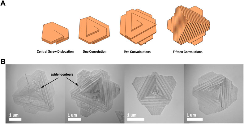
FIGURE 1. (A) An illustration of the growth process of spiral Sb2Te3 nanoplates. (B) A selection of TEM images showing spiral Sb2Te3 nanoplates of slightly different sizes and morphologies, some with spider-contours.
Growth of spiral Sb2Te3 nanoplates by SLS method was first achieved in a recent paper by Dun et al. (2017), which serves as a foundational work for this study. In their paper, Dun et al. not only grew these topologically complex nanoplates, but further used the dangling tellurium bonds on the active nanoplate edges as heterogeneous nucleation sites, growing small silver (Ag) nanoparticles. The resulting Ag-decorated spiral nanoplates were then used to construct flexible thermoelectric thin films that remarkably saw a decoupled electrical conductivity and Seebeck effect. These thin films were measured to have a power factor of 371 μW m−1 K−2 and a figure of merit ZT of 0.23.
The present study further develops the synthesis procedure put forth by Dun et al. (2017) in order to produce Sb2Te3 spiral nanoplate MSLs. We additionally detail a procedure that produces spiral nanoplates with a central nanopore, caused by tandem growth with nanorods. Emphasis is given to modifications of the typical reaction procedure that lead to visible and controllable changes in the resulting nanocrystals. The crystal growth process and conditions necessary for the screw dislocation-driven growth of Sb2Te3 are also explored in this study. We propose that further research could yield a synthesis procedure for Sb2Te3 MSLs with a twist angle that is controlled by tuning reaction parameters. Such a development could allow large scale production of Sb2Te3 MSLs, ready for use in electronic systems.
2 Materials and methods
2.1 Synthesis of Sb2Te3 spiral-type nanoplates
The reaction that creates Sb2Te3 spiral-type nanoplates (Figure 1B and Figure 2) takes place in one three-necked flask under reflux. Reactants 9 mmol of tellurium oxide (TeO), 6 mmol of antimony chloride (SbCl3), 1.46 g of sodium hydroxide (NaOH), and 800 mg of Polyvinylpyrrolidone (PVP) are dissolved into 70 ml of ethylene glycol (EG) one by one. Air is evacuated from the flask and replaced with argon gas. The flask is heated with a heating mantle to 130°C and held at this temperature for 10 min. In this time, the solution should turn black. Then, 8 ml hydrazine hydrate (N2H4) is pumped into the flask at a pace of 2.5 ml per minute. The solution is then left to stir at 130°C for 3 hours before it is further heated to 160°C and left for an additional 15 h. In this time, the solution should lighten a bit to an opaque gray. Heating is then stopped, and the flask is left to cool.
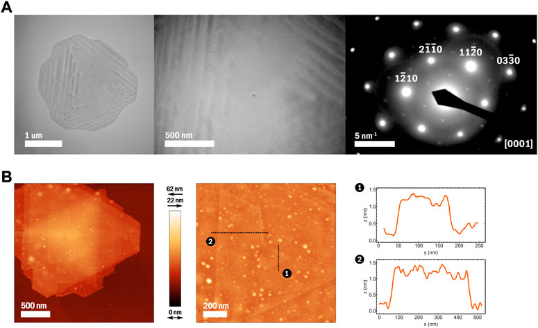
FIGURE 2. (A) TEM images and corresponding SAED pattern of an Sb2Te3 spiral nanoplate with a visible core. (B) AFM images and height profile plots of an Sb2Te3 spiral nanoplate showing the crystal steps to be 1 nm thick.
At this stage, the nanoplates have formed and are well-coated with PVP, much of which must be washed away for successful edge doping, imaging, or other applications. Once the flask is cool, the solution is divided into four centrifuge tubes. These tubes are then filled with acetone, and the nanoplates are collected into pellets by centrifugation at 5000 rpm for 20 min. The supernatant is discarded, after which the pellets are dispersed into 20 ml of ethanol by crushing with a glass stir rod, by vortexing, and by bath sonicating in water. This process is repeated by again by filling the tubes with acetone, followed by centrifugation. In this manner, the nanoplates are washed three to six times.
2.2 Synthesis of hexagonal Sb2Te3 nanoplates
The reaction that creates hexagonal Sb2Te3 nanoplates (Figure 3) is identical to that of Section 2.1 with one exception. The 8 ml of N2H4 is added at a rapid, unregulated pace before heating begins.
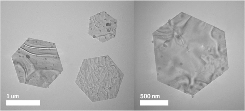
FIGURE 3. TEM images of flat, hexagonal Sb2Te3 nanoplates.
2.3 Synthesis of Sb2Te3 spiral-type nanoplates with moiré patterns
The reaction that creates Sb2Te3 spiral-type nanoplates with moiré patterns (Figure 4) uses two three-necked flasks, joined with a distillation adapter. One flask is placed under reflux (Flask A). In Flask A, the same reactants as listed in Section 2.1 are dissolved into 70 ml of EG. An additional 1.5 ml of EG is placed in the remaining flask (Flask B). Air is then evacuated from the setup and replaced with argon gas. Both flasks are heated simultaneously to 130°C. Then, 8 ml of N2H4 is pumped into Flask B, such that it begins to vaporize and is slowly delivered as a vapor into Flask A. The solution is then left to stir at 130°C for 3 hours before it is further heated to 160°C and left for an additional 15 h. The heating is then stopped, the flasks are left to cool, and the resulting nanoplates are collected and washed as described in Section 2.1.
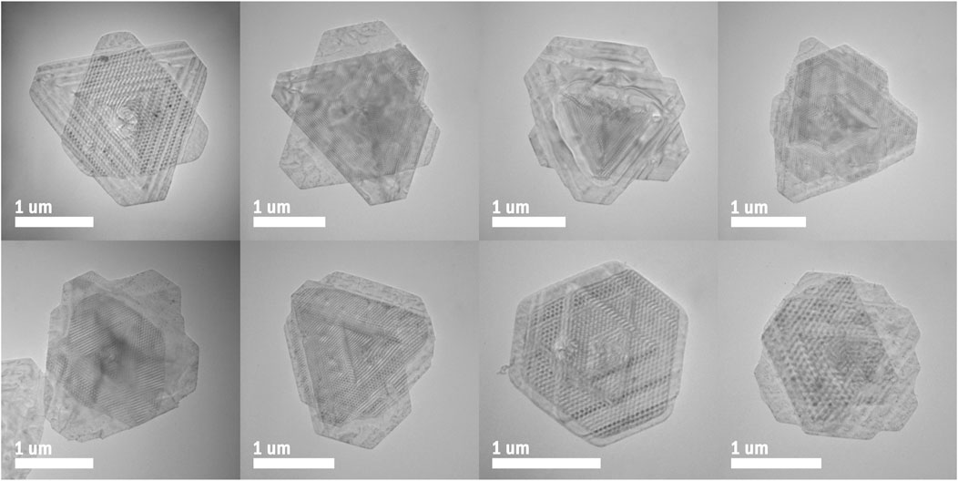
FIGURE 4. TEM images of Sb2Te3 spiral nanoplates, each with a visible moiré pattern.
2.4 Synthesis of Sb2Te3 spiral-type nanoplates with central nanopores
The reaction that creates Sb2Te3 spiral-type nanoplates with central nanopores (Supplementary Figure S1B) is identical to that of Section 2.3 with one exception. Into Flask B is added 30 ml of EG instead of 1.5 ml. This is done to further slow the rate of addition of N2H4 into Flask A.
2.5 Sample characterization methods
Analysis of results from various reactions is performed by thorough examination of material sample images captured using a JEOL 1200-EX TEM equipped with a SIA-L3 camera. SAED analysis is also performed with the same machine. SAED image analysis was performed in CrysTBox. The AFM analysis in this study was performed by a Veeco Nanoscope IIIa Multimode in tapping mode. AFM image analysis was performed in Gwyddion. Moiré pattern simulation was performed by custom code written in Wolfram Mathematica, and TEM direct image analysis was performed using ImageJ.
3 Results and discussion
3.1 Spiral characterization results
Synthesized as described in Section 2.1; Figure 1B shows a selection of Sb2Te3 spiral-type nanoplates. The growth of these nanoplates is driven by a central screw dislocation, causing the typically many-layered structure of Sb2Te3 to instead form one continuous layer that spirals into a third dimension (Dun et al., 2017). Figure 1A illustrates how one screw dislocation is integral to this structural change. Given our colloidal synthesis method, and thus lack of substrate, the spiral-type nanoplates grow similarly on both sides, with a morphology like that of a trigonal bipyramid. Spider-contours are visible on many of these nanoplates (Figure 1B), often positioned at their center, which likely result from the strain field caused by screw dislocations (Morin et al., 2011). These nanoplates have been measured to range between 4μm2 and 10 μm2 in area. Selected area electron diffraction (SAED) analysis of Sb2Te3 spiral-type nanoplates (Figure 2A) reveals an interplanar spacing of 0.213 nm for planes (11
Careful and deliberate modification of synthesis procedures revealed that the quantity and rate of N2H4 addition greatly impacts the morphology of the resulting nanomaterials. Without N2H4, only nanorods form. When N2H4 is added with the other reactants, all at once before heating, screw dislocation-driven growth is not observed. Instead, flat hexagonal Sb2Te3 nanoplates with a typical area of about 1.5 μm2 are formed (Figure 3). The slower addition of N2H4 as a vapor, described in Section 2.3, frequently produces spiral nanoplates that exhibit moiré patterns (Figure 4). We propose that the presence of these patterns is due to increased strain within the central screw dislocation, resulting in a relative twist angle between spiral steps. While each spiral has many vdW gaps, observed moiré patterns are typically characteristic of a twist across only one gap, allowing interpretation of these patterns to be consistent with those produced by twisted bilayer Sb2Te3.
We performed a simulation in order to characterize the relationship between relative twist angle (θ) and moiré fringe spacing in bilayer Sb2Te3. A custom code was written that directly plots two lattices with a relative twist angle using graphics objects. Each lattice represents Sb2Te3’s five atomic sheet structure as seen from the [0001] zone axis. The scale of this plot is determined using the accepted values for the lattice constants of Sb2Te3. The resulting moiré pattern is then made more pronounced with careful use of uniform image filtering (Figure 5A). An isometric grid is fit to the set of brightest pixels within this plot, from which nearest neighbor spacing (s) was measured. This process was repeated for several values of θ, and from the resulting data was found the following best-fit equation with a root-mean-square error (RSME) of 0.032 nm (Figure 5B).
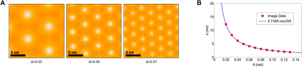
FIGURE 5. (A) Three simulated Sb2Te3 moiré patterns at increasing twist angles. (B) Plot showing both the simulated image data and the best-fit curve.
With a choice of 0 < θ < π/6, this best-fit equation is easily inverted to estimate the twist angle of the Sb2Te3 MSLs observed with TEM. Moiré fringe spacing was measured from TEM images in agreement with our simulation: by fitting a nearest-neighbor grid to the dark spots of an MSL (Figure 6A). From this grid is produced a distribution of lengths (Figure 6B), from which is extracted an average value for s and its error. Using our equation obtained from simulation, θ values are then estimated. Twenty MSLs were analyzed in this manner; between nanoplates, θ values ranged from 0.14° to 0.52° and measurement error never exceeded 0.2%. Additional detail is provided in the Supplementary Materials. Twist angles in vdW materials have also been effectively measured using SAED pattern analysis (Liu et al., 2019). In our case, the reported twist angles are too small to be properly quantified using this method (Supplementary Figure S6).
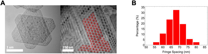
FIGURE 6. (A) TEM images of an Sb2Te3 nanoplate with a visible moiré pattern. A nearest-neighbor grid is marked in red. (B) A histogram showing the distribution of side lengths in this nearest-neighbor grid. A fringe spacing of 67.60 ± 0.05 nm is determined from this data, and thus an estimated twist angle of 0.2074 ± 0.0003°.
To observe the nanoplate growth process directly, samples were extracted from early stages of synthesis and examined with TEM. Minutes after heating begins, nanorods form in solution, turning the solution black. Nanoplates then nucleate and grow at the tips of these nanorods in the following few hours of heating (Supplementary Figure S4). Interestingly, this process is analogous to the vapor-phase snowflake growth performed by Libbrecht (2005), wherein the growth phases of ice were manipulated to form plate-like crystals at the tips of ice needles. By the time heating is switched off in the syntheses described in Sections 2.1–2.3, these nanorods have mostly redissolved into solution. However, in the synthesis described in Section 2.4, these nanorods instead persist and thicken as shown in Supplementary Figure S1A. During this synthesis, nanoplates frequently become separated from the thickened nanorods, often leaving the nanoplate with a central nanopore as seen in Supplementary Figure S1B. These nanopores are typically circular and range from 20 to 25 nm in diameter.
4 Conclusion
In this study, we have demonstrated a viable chemical route to the formation of moiré materials based on multilayer 2D chalcogenides by leveraging screw dislocation-driven growth. We observed twist angles up to 0.52° utilizing high-resolution microscopy and simulation. We suggest that the presence of moiré patterns in Sb2Te3 spiral-type nanoplates is due to increased strain within the central screw dislocation, and that this strain has been modulated by changes to the rate and method of N2H4 addition during synthesis. Further exploration may lead to precise chemical control over the resulting twist angle. Given that the syntheses put forward in this study are simple and scalable, we believe that this approach to moiré patterns in spiral-type Sb2Te3 nanoplates could represent an exciting new way to create twistronic systems, ready for use in electronic devices.
Data availability statement
The raw data supporting the conclusion of this article will be made available by the authors, without undue reservation.
Author contributions
RL wrote the manuscript, performed computations, and created the figures. RL and GM developed synthesis methods. DC coordinated the project. All authors have discussed the results, contributed to manuscript revision, and have approved the submitted version.
Funding
The Carroll lab was provided by Streamline Automation: U.S. Department of Defense/Air Force under Grant No. GR-00000327.
Acknowledgments
We would like to thank Martin Guthold and Stephen Baker for allowing us access to their equipment and for their work gathering AFM data.
Conflict of interest
The authors declare that the research was conducted in the absence of any commercial or financial relationships that could be construed as a potential conflict of interest.
Publisher’s note
All claims expressed in this article are solely those of the authors and do not necessarily represent those of their affiliated organizations, or those of the publisher, the editors and the reviewers. Any product that may be evaluated in this article, or claim that may be made by its manufacturer, is not guaranteed or endorsed by the publisher.
Supplementary material
The Supplementary Material for this article can be found online at: https://www.frontiersin.org/articles/10.3389/fmats.2022.963775/full#supplementary-material
References
Cao, Y., Fatemi, V., Demir, A., Fang, S., Tomarken, S. L., Luo, J. Y., et al. (2018). Correlated insulator behaviour at half-filling in magic-angle graphene superlattices. Nature 556 (7699), 80–84. doi:10.1038/nature26154
Cao, Y., Fatemi, V., Fang, S., Watanabe, K., Taniguchi, T., Kaxiras, E., et al. (2018). Unconventional superconductivity in magic-angle graphene superlattices. Nature 556 (7699), 43–50. doi:10.1038/nature26160
Chen, L., Liu, B., Abbas, A. N., Ma, Y., Fang, X., Liu, Y., et al. (2014). Screw-dislocation-driven growth of two-dimensional few-layer and pyramid-like WSe 2 by sulfur-assisted chemical vapor deposition. ACS Nano 8 (11), 11543–11551. doi:10.1021/nn504775f
Dun, C., Hewitt, C. A., Li, Q., Xu, J., Schall, D. C., Lee, H., et al. (2017). 2D chalcogenide nanoplate Assemblies for thermoelectric applications. Adv. Mat. 29 (21), 1700070. doi:10.1002/adma.201700070
He, F., Zhou, Y., Ye, Z., Cho, S. H., Jeong, J., Meng, X., et al. (2021). Moiré patterns in 2D materials: A review. ACS Nano 15 (4), 5944–5958. doi:10.1021/acsnano.0c10435
Hennighausen, Z., Lane, C., Buda, I. G., Mathur, V. K., Bansil, A., and Kar, S. (2019). Evidence of a purely electronic two-dimensional lattice at the interface of TMD/Bi 2 Se 3 heterostructures. Nanoscale 11 (34), 15929–15938. doi:10.1039/C9NR04412D
Lau, C. N., Bockrath, M. W., Mak, K. F., and Zhang, F. (2022). Reproducibility in the fabrication and physics of moiré materials. Nature 602 (7895), 41–50. doi:10.1038/s41586-021-04173-z
Li, H., Li, S., Regan, E. C., Wang, D., Zhao, W., Kahn, S., et al. (2021). Imaging two-dimensional generalized Wigner crystals. Nature 597 (7878), 650–654. doi:10.1038/s41586-021-03874-9
Libbrecht, K. G. (2005). The physics of snow crystals. Rep. Prog. Phys. 68 (4), 855–895. doi:10.1088/0034-4885/68/4/R03
Liu, J., Huang, Q., Qian, Y., Huang, Z., Lai, F., Lin, L., et al. (2016). Screw dislocation-driven growth of the layered spiral-type SnSe nanoplates. Cryst. Growth & Des. 16 (4), 2052–2056. doi:10.1021/acs.cgd.5b01708
Liu, L., Sun, Y., Cui, X., Qi, K., He, X., Bao, Q., et al. (2019). Bottom-up growth of homogeneous Moiré superlattices in bismuth oxychloride spiral nanosheets. Nat. Commun. 10 (1), 4472. doi:10.1038/s41467-019-12347-7
Morin, S. A., Forticaux, A., Bierman, M. J., and Jin, S. (2011). Screw dislocation-driven growth of two-dimensional nanoplates. Nano Lett. 11 (10), 4449–4455. doi:10.1021/nl202689m
Keywords: moiré pattern, chalcogenide, topological insulator, quantum material, one pot synthesis, twistronics, screw dislocation, van der waals materials
Citation: Link R, Marcus G and Carroll D (2022) Solvothermal growth of moiré superlattices in antimony telluride spiral-type nanoplates. Front. Mater. 9:963775. doi: 10.3389/fmats.2022.963775
Received: 07 June 2022; Accepted: 03 October 2022;
Published: 20 October 2022.
Edited by:
Mingliang Tian, Hefei Institutes of Physical Science (CAS), ChinaReviewed by:
Deepak K. Pandey, KICVentures Group - The LES Institute, United StatesXue Liu, Anhui University, China
Copyright © 2022 Link, Marcus and Carroll. This is an open-access article distributed under the terms of the Creative Commons Attribution License (CC BY). The use, distribution or reproduction in other forums is permitted, provided the original author(s) and the copyright owner(s) are credited and that the original publication in this journal is cited, in accordance with accepted academic practice. No use, distribution or reproduction is permitted which does not comply with these terms.
*Correspondence: David Carroll, Y2Fycm9sZGxAd2Z1LmVkdQ==