 Shuting Zhao
 Yibin Yang
 Xing Feng
 Yu Zhao
- Guangdong Provincial Key Laboratory of Information Photonics Technology, Guangdong Provincial Key Laboratory of Functional Soft Condensed Matter, School of Materials and Energy, Guangdong University of Technology, Guangzhou, China
Due to its good p-type semiconductor characteristics, MnSe has a great application prospect in high-performance electronic and optoelectronic devices. However, heterojunctions of MnSe still need to be deeply studied to improve its electrical and photoelectric properties. Here, it is reported that the two-dimensional (2D) MnSe/WSe2 heterojunction is structured by the non-layered MnSe nanosheets synthesized by chemical vapor deposition (CVD) method and the mechanically exfoliated layered WSe2. The heterojunction device exhibits a rectification effect and a current on/off ratio of 6,557. Meanwhile, it has a broad spectral range response from ultraviolet (UV) to short-wave infrared radiation (SWIR) (300–2,200 nm), and achieves an ultra-high responsivity of 156 A/W, along with an excellent detectivity of 2.21 × 10¹² jones, and an outstanding external quantum efficiency (EQE) of 36,400%. Moreover, the type II band alignment and the built-in potential in the MnSe/WSe2 heterojunction can facilitate the separation of the photoexcited electron-hole pairs, which enables the significant photovoltaic characteristics and self-powered photoswitching response. This work reveals the novel performance of the 2D MnSe/WSe2 heterojunction and a great potential in photoswitching, photodetector, and photovoltaic applications.
Introduction
Since monolayer graphene was successfully stripped and proved to have extraordinary electrical transmission properties in 2004 (Novoselov et al., 2004), ultrathin two-dimensional (2D) materials have ushered in a research boom. So far, 2D layered materials have developed into a large family, including black phosphorus (BP) (Li et al., 2014; Guo et al., 2016; Guo et al., 2017), hexagonal boronnitride (h-BN) (Gorbachev et al., 2011), and transition metal dichalcogenides (TMDs) (Matte et al., 2010; Radisavljevic et al., 2011; Jariwala et al., 2014; Tan and Zhang, 2015; Ouyang et al., 2021). Their unique structural characteristics make them have tunable electronics, novel optical properties and good mechanical properties, thus attracting a lot of research (Hafeez et al., 2016; Manzeli et al., 2017; Cao et al., 2022a). In addition, the synthesis and applications of 2D non-layered materials have also received extensive attention, which possess different properties compared with 2D layered materials. 2D non-layered materials are connected by strengthened chemical bonds of atoms, with a large number of unsaturated dangling bonds on the surface, which induces a high-activity and high-energy surface. Meanwhile, they have the characteristics of both bulk structures and 2D structures (Zhou et al., 2019; Cao et al., 2022b). Therefore, The in-depth study of 2D non-layered materials will deepen our understanding and promote their applications in electronics, optoelectronics, catalysis and other fields.
2D MnSe is a non-layered p-type semiconductor, which has been successfully prepared in recent years (Zheng et al., 2019). Due to its unique properties in magnetism and photoelectric detection, MnSe has a broad application prospect in spintronic devices and photodetectors, which has attracted the strong interest of many researchers. For example, Li et al. (2021) synthesized α-MnSe nanosheets on mica substrates by the APCVD method. Zhou et al. (2022) prepared MnSe flakes by space-limited CVD method. Zhang et al. (2021) successfully synthesized ultrathin α-MnSe nanosheets by a salt-assisted vdWE growth method. However, devices made of one single material usually have disadvantages such as low light absorption, large dark current and low detection rate. Fortunately, These problems can be effectively solved by 2D van der Waals (vdW) heterojunctions. For instance, α-MnSe/WS2 2D heterojunctions were synthesized, which showed an excellent photo detectivity of 1.00 × 10¹³ Jones and photo responsivity of 49.1 A/W (Zhang et al., 2021). On the other hand, WSe2 is a bipolar semiconductor with an indirect band gap of 0.9–1.6 eV (Nourbakhsh et al., 2016; Zhou et al., 2018; Gao et al., 2019; Xu et al., 2021). The field-effect transistors (FETs) with a small number of layers of WSe2 achieved a carrier mobility of up to 70.1 cm2 V−1s−1 and open-light ratio of over 106, using Al2O3 as the top gate (Liu et al., 2013). Therefore, heterojunctions formed by stacking WSe2 and other 2D materials will help to improve the electronic and optoelectronic performance (Feng et al., 2022; Luo et al., 2022).
In this work, the 2D MnSe/WSe2 heterojunction is structured by the non-layered MnSe nanosheets synthesized by CVD method and the mechanically exfoliated layered WSe2. The heterojunction device exhibits a rectification effect and a current on/off ratio of 6,557. Meanwhile, it has a broad spectral range response from UV to SWIR (300–2,200 nm), and achieves an ultra-high responsivity of 156 A/W, along with an excellent detectivity of 2.21 × 10¹² jones, and an outstanding EQE of 36,400%. Furthermore, due to the type II band alignment and the built-in potential in the MnSe/WSe2 heterojunction, photogenerated carriers (electron-hole pairs) are effectively separated when the light radiates the p-n junction, which enables the significant photovoltaic characteristics and self-driven photoswitching response.
Experimental
Materials
A certain amount of Se powder (99.99%, Alfa) was weighed and placed in a quartz boat and then placed in the upstream of a single temperature zone vacuum tube furnace. A small amount of MnCl2 (99.99%, Alfa), a trace of NaCl and clean fluorine gold mica flakes were placed in the center of the quartz tube at a constant temperature zone (640°C). After blowing away the air in the quartz tube of the CVD furnace by 100 sccm argon for 1 hour, the gas flow rate was maintained at 60 sccm. The heating program was set to heat the central heating zone from room temperature to 640°C at a rate of 30°C/min, followed by holding for 10–15 min and cooling naturally to room temperature.WSe2 nanosheets were prepared by mechanical exfoliation method using the blue tape (UST, America), and transferred to the Si/SiO2 substrate.
Device fabrications
The PS solution (polystyrene dissolved in toluene) was spin-coated on the WSe2 on Si/SiO2 substrate. After drying at 90°C for 15 min, the PS film with WSe2 nanosheets (PS film/WSe2) was peeled off the Si/SiO2 substrate, attached to the polydimethylsiloxane (PDMS) film and transferred to MnSe on mica substrate to form the MnSe/WSe2 heterojunction. The sample was immersed in toluene to dissolve the PS film. 50-nm-thick Au as electrodes were deposited by a standard photolithography process and thermal evaporation. The above manufacturing process is shown in Supplementary Figure S1. For the fabrication of top gate device, the h-BN was transferred to cover the MnSe/WSe2 heterojunction, followed by the deposition of Au electrodes.
Characterizations
Optical microscopy (Motic, BA310Met), atomic force microscopy (AFM) (Bruker, Dimension FastScan), Raman (NOST, FEX, 532 nm excitation laser), high-resolution transmission electron microscopy (HRTEM) (FEI, Thermo, Talos F200S), X-ray diffraction (XRD) (Bruker, D8 VENTURE) and X-ray photoelectron spectroscopy (XPS) (Thermo Fisher, Escalab 250Xi) were used to characterize the morphology, thickness, surface potential and microstructure of the materials. The electric and photoelectric properties were characterized by the source meter (Keithley, 2636B). The photo response was measured in air at room temperature, under 300, 405, 532, 635, 808, 1,060, 1,310, 1,550, and 2,200 nm lasers, respectively.
Results and Discussion
Figure 1A shows that the 2θ peaks of the XRD plot of MnSe appear at 28.3°, 32.8°, 47.0°, 58.5° and 68.7°, respectively. The two main diffraction peaks are 28.3° and 58.5°, corresponding to the cubic (111) and (222) crystallographic planes of α-MnSe in comparison of the PDF no.11-0683, which reveals that the MnSe was grown along the <111> direction. The surface elemental composition and chemical state of the synthesized samples were further investigated by XPS, as shown in Figure 1B. The peaks at 653.53 and 641.8eV in the XPS pattern belong to Mn 2p1/2 and Mn 2p3/2, respectively. A binding energy separation value of 11.73 eV can be determined as Mn2+ (Li et al., 2021). While the peaks at 656.84 eV and 646.05 come from the weak surface oxidization (Hu et al., 2020). In addition, the peaks at 55.05 and 54.2 eV binding energies are attributed to Se 3d3/2 and 3d5/2, indicating the existence of Se2- (Li et al., 2021), while the peaks at 56 and 53.4 eV are due to the weak oxidation of the surface layer (Zhou et al., 2022). The HRTEM image in Figure 1C clearly shows two planar spacings of 0.11 and 0.19 nm, which are in good agreement with the (4
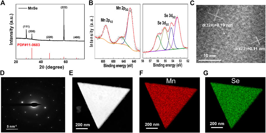
FIGURE 1. Material characterizations of the synthesized MnSe nanosheets. (A) XRD pattern. (B) XPS patterns. (C) HRTEM image and (D) SAED pattern. (E) TEM image. EDS patterns of (F) Mn and (G) Se in the synthesized MnSe nanosheets.
Figures 2A, B exhibit the optical microscopy and structure diagram of MnSe/WSe2 heterojunction, with an effective channel area of 67.9 μm2. Information on the lattice vibrational modes and phase structure can be learned from the Raman spectra. The Raman spectra of MnSe nanosheets, WSe2 nanosheets and the MnSe/WSe2 heterostructure of the same device are shown in Figure 2C. It is clearly seen that there is only one significant Raman peak at 253.3 cm-1 for MnSe. Two main Raman peaks of WSe2 are located at 246.6 and 254.9 cm-1, which are attributed to the E12g and A1g modes, respectively (Hu et al., 2017; Sun et al., 2020). The Raman peaks of the heterojunction are consistent with those of the two constituent materials, which indicates the effective combination of phonon vibration modes of two constituent materials. The AFM image of the MnSe/WSe2 heterojunction in Figure 2D displays the thicknesses of MnSe and WSe2 nanosheets are 90 and 102 nm, respectively.
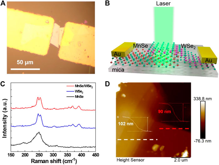
FIGURE 2. (A) The optical microscope image and (B) the schematic diagram of the MnSe/WSe2 heterostructure. (C) The Raman spectra of MnSe, WSe2 and MnSe/WSe2 heterostructure, respectively. (D) AFM image of MnSe/WSe2 interface with insets of their height profiles.
The conductivity types of MnSe and WSe2 were experimentally measured as p-type and bipolar conductivity, respectively, shown in Supplementary Figure S3. To obtain the built-in contact potential difference at the interface between MnSe and WSe2, Kelvin probe force microscopy (KPFM) measurements were performed. Supplementary Figure S4 exhibits the surface potential distribution (SPD) of WSe2 and MnSe nanosheets in the tip region of AFM, which can be expressed as the following equations:
where e is the electron charge,
Thus, the difference of the work function between MnSe and WSe2 is about 130 mV, which is illustrated by the potential height profile near the interface of the MnSe/WSe2 heterojunction shown in the inset of Supplementary Figure S4. To elucidate the band alignment of MnSe/WSe2 heterojunction, calculations are performed via using the projector-augmented plane-wave (PAW) method within the work of density functional theory (DFT) in VASP. 1 × 1×2 supercells of both MnSe and WSe2 are constructed. A vacuum of about 25 Å is applied to eliminate the interaction between adjacent images for the calculation of 2D structure. Due to the existence of 3d orbitals of Mn atoms, magnetism is taken into account in the DFT calculation. The calculated band structures of 2D MnSe and WSe2 are shown in Figure 3A, with the Fermi level set as zero. According to the calculated results, band alignments of MnSe and WSe2 before contact are displayed in Figure 3B, which indicates a type II heterostructure. Therefore, to further investigate the electrical characteristics, the MnSe/WSe2 FET with h-BN top gate was fabricated, with MnSe as source and WSe2 as drain electrodes; Figure 3C shows the Ids-Vds curve under Vg = 0 V (the semi-logarithmic form shown in Supplementary Figure S5A), which demonstrates a clear current rectification effect and the rectification ratio is 18 under Vds of 8 and -8 V. Figure 3D displays the transfer characteristic curve of the MnSe/WSe2 FET (the semi-logarithmic form shown in Supplementary Figure S5B), which suggests that this FET is a p-type conduction. Under the Vds of 5 V, the current on/off ratio can reach as high as 6,557.
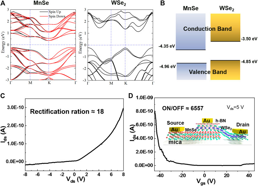
FIGURE 3. (A) Calculated band structures of 2D MnSe and WSe2, respectively. (B) Band alignments of MnSe and WSe2 before contact. (C) The Ids–Vds characteristic curve at Vg = 0 V and (D) the transfer curve at Vds = 5 V of the MnSe/WSe2 heterojunction FET with h-BN top gate.
To investigate the optical response performance of the MnSe/WSe2 heterojunction device, the photocurrents were measured at Vds = 5 V and under 300–2,200 nm laser irradiation periodically, respectively. The results for 405, 532, 635 and 808 nm are shown in Figures 4A–D, while 300, 1,060, 1,310, 1,550 and 2,200 nm are shown in Supplementary Figures S6, S7. These results clearly illuminate that the MnSe/WSe2 heterojunction device has a broad spectral range response from UV to SWIR. Moreover, the photo response performance of the device is evaluated using three key photodetector parameters: responsivity (Rλ), detectivity (D*), and EQE. Rλ refers to the photocurrent generated per unit power of incident light per unit area of the photoelectric device, and is used to measure an important indicator of the photoelectric conversion efficiency of the device, which is expressed by the following equation:
where
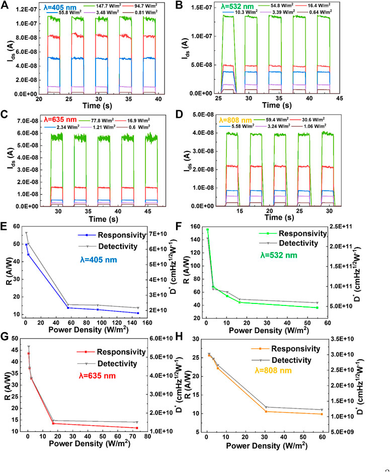
FIGURE 4. The photo response of the MnSe/WSe2 heterojunction at Vds = 5 V and Vg = 0 V under the irradiation of (A) 405 nm, (B) 532 nm, (C) 635 nm and (D) 808 nm laser, respectively, with different light power intensities. The light-power-dependent responsivity and detectivity under the irradiation of (E) 405 nm, (F) 532 nm, (G) 635 nm and (H) 808 nm laser, respectively.
EQE is the number of electron-hole pairs excited by one incident photon with expression as follows:
where h is Planck’s constant; c is the light velocity and
The
The photovoltaic characteristics of the MnSe/WSe2 heterojunction are investigated, as shown in Figure 5A, which shows the Ids-Vds curves under dark and 405 nm laser irradiation, respectively. The photocurrent generated at zero bias as short-circuit current (Isc) and the photovoltage generated at zero current is defined as open-circuit voltage (Voc), respectively. It can be seen that the Isc and Voc are 32.1 pA and 0.16 V, respectively, under a laser power of 3.47 W/m2.The electrical output power Pel is given by the equation
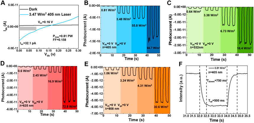
FIGURE 5. (A) Ids-Vds curve at zero bias, under dark and 405 nm laser irradiation, respectively. The photocurrent at different optical power intensities in response to (B) 405 nm, (C) 532 nm, (D) 635 nm and (E) 808 nm lasers, respectively. (F) Rise and fall time of the MnSe/WSe2 heterojunction device under zero bias and 405 nm laser irradiation.
The point in the Ids-Vds curve that has the maximum electrical output power Pmax can be found in the rectangle in Figure 5A. The fill factor (FF) is expressed as
As a result, Pmax and FF are calculated to be 0.81 pW and 0.158, respectively.
When under the zero-bias state (Vds = 0V, Vgs = 0V), the MnSe/WSe2 heterojunction operates in photovoltaic mode. Figures 5B–E exhibit the optical response as a self-powered photodetector under different optical power of 405, 532, 635 and 808 nm laser irradiation, respectively, which illustrates an obvious self-driven photoswitching effect. The rise and fall times are 500 and 750 ms, respectively, as shown in Figure 5F. The photocurrent is 1 pA and the dark current is 0.03 pA under 405 nm laser irradiation with the intensity of 0.81 W/m2. By calculation, Rλ, D* and EQE are 148 mA/W, 2.74 × 10¹⁰ jones and 45.4%, respectively. These results proves that the MnSe/WSe2 heterojunction is a high-performance self-powered photodetector, compared with other reported 2D heterojunctions (see Supplementary Table S1).
Conclusion
In summary, we synthesized 2D non-layered MnSe nanosheets with high crystal quality by CVD method, mechanically exfoliated layered WSe2 nanosheets, and structured the MnSe/WSe2 heterojunction. The heterojunction device exhibits a rectification effect and a current on/off ratio of 6,557. Meanwhile, it has a broad spectral range response from UV to SWIR (300–2,200 nm), and achieves an ultra-high responsivity of 156 A/W, along with an excellent detectivity of 2.21 × 10¹² jones, and an outstanding EQE of 36,400%. Moreover, the type II band alignment and the built-in potential in the MnSe/WSe2 heterojunction can facilitate the separation of the photoexcited electron-hole pairs, which enables the significant photovoltaic characteristics and sensitive self-powered photoswitching response. This work reveals the novel performance of the 2D MnSe/WSe2 heterojunction and a great potential in photoswitching, photodetector, and photovoltaic applications.
Data availability statement
The original contributions presented in the study are included in the article/Supplementary Materials, further inquiries can be directed to the corresponding authors.
Author contributions
YZ conceived and supervised the project. YY discussed the results and revised the paper. SZ prepared and characterized the material, fabricated the full devices, and tested the devices performance. XC conducted materials research to help prepare devices and tests. ZL participated in characterization results and other data analysis. LT, ZZ, and XF reviewed the paper. This manuscript is the result of discussion by all authors. All authors approved the final version of the manual.
Funding
This work was sponsored by the National Natural Science Foundation of China (Grant no. 61975036), the Fund of Guangdong Provincial Key Laboratory of Information Photonics Technology (Grant no. 2020B121201011).
Conflict of interest
The authors declare that the research was conducted in the absence of any commercial or financial relationships that could be construed as a potential conflict of interest.
Publisher’s note
All claims expressed in this article are solely those of the authors and do not necessarily represent those of their affiliated organizations, or those of the publisher, the editors and the reviewers. Any product that may be evaluated in this article, or claim that may be made by its manufacturer, is not guaranteed or endorsed by the publisher.
Supplementary material
The Supplementary Material for this article can be found online at: https://www.frontiersin.org/articles/10.3389/fmats.2023.1162166/full#supplementary-material
References
Cao, X. H., Lei, Z. H., Huang, B. Q., Wei, A. X., Tao, L. L., Yang, Y. B., et al. (2022). Non-layered Te/In2S3 tunneling heterojunctions with ultrahigh photoresponsivity and fast photoresponse. Small 18 (18), 2200445. doi:10.1002/smll.202200445
Cao, X. H., Lei, Z. H., Zhao, S. T., Tao, L. L., Zheng, Z. Q., Feng, X., et al. (2022). Te/SnS2 tunneling heterojunctions as high-performance photodetectors with superior self-powered properties. Nanoscale Adv. 4 (20), 4296–4303. doi:10.1039/d2na00507g
Feng, P., He, S. X., Zhao, S. X., Dang, C. C., Li, M., Zhao, L. C., et al. (2022). A high-performance self-powered photodetector based on WSe2-graphene-MoTe2 van der Waals heterojunctions. J. Mat. Chem. C 10 (24), 9401–9406. doi:10.1039/d2tc01441f
Gao, W., Zhang, F., Zheng, Z. Q., and Li, J. B. (2019). Unique and tunable photodetecting performance for two-dimensional layered MoSe2/WSe2 p-n junction on the 4H-SiC substrate. ACS Appl. Mat. Interfaces 11 (21), 19277–19285. doi:10.1021/acsami.9b03709
Gorbachev, R. V., Riaz, I., Nair, R. R., Jalil, R., Britnell, L., Belle, B. D., et al. (2011). Hunting for monolayer boron nitride: Optical and Raman signatures. Small 7 (4), 465–468. doi:10.1002/smll.201001628
Guo, Q. S., Pospischil, A., Bhuiyan, M., Jiang, H., Tian, H., Farmer, D., et al. (2016). Black phosphorus mid-infrared photodetectors with high gain. Nano Lett. 16 (7), 4648–4655. doi:10.1021/acs.nanolett.6b01977
Guo, Z. N., Chen, S., Wang, Z. Z., Yang, Z. Y., Liu, F., Xu, Y. H., et al. (2017). Metal-ion-modified black phosphorus with enhanced stability and transistor performance. Adv. Mat. 29 (42), 1703811. doi:10.1002/adma.201703811
Hafeez, M., Gan, L., Li, H. Q., Ma, Y., and Zhai, T. Y. (2016). Chemical vapor deposition synthesis of ultrathin hexagonal ReSe2 flakes for anisotropic Raman property and optoelectronic application. Adv. Mat. 28 (37), 8296–8301. doi:10.1002/adma.201601977
Hu, C., Dong, D. D., Yang, X. K., Qiao, K. K., Yang, D., Deng, H., et al. (2017). Synergistic effect of hybrid PbS quantum dots/2D-WSe2 toward high performance and broadband phototransistors. Adv. Funct. Mat. 27 (2), 1603605. doi:10.1002/adfm.201603605
Hu, L., He, L. Q., Wang, X., Shang, C. Q., and Zhou, G. F. (2020). MnSe embedded in carbon nanofibers as advanced anode material for sodium ion batteries. Nanotechnology 31 (33), 335402. doi:10.1088/1361-6528/ab8e78
Jariwala, D., Sangwan, V. K., Lauhon, L. J., Marks, T. J., and Hersam, M. C. (2014). Emerging device applications for semiconducting two-dimensional transition metal dichalcogenides. ACS Nano 8 (2), 1102–1120. doi:10.1021/nn500064s
Li, L. K., Yu, Y. J., Ye, G. J., Ge, Q. Q., Ou, X. D., Wu, H., et al. (2014). Black phosphorus field-effect transistors. Nat. Nanotechnol. 9 (5), 372–377. doi:10.1038/nnano.2014.35
Li, N. N., Zhu, L. L., Shang, H. H., Wang, F., Zhang, Y., Yao, Y. Y., et al. (2021). Controlled synthesis and Raman study of A 2D antiferromagnetic P-type semiconductor: Alpha-MnSe. Nanoscale 13 (14), 6953–6964. doi:10.1039/d1nr00822f
Liu, W., Kang, J. H., Sarkar, D., Khatami, Y., Jena, D., and Banerjee, K. (2013). Role of metal contacts in designing high-performance monolayer n-type WSe2 field effect transistors. Nano Lett. 13 (5), 1983–1990. doi:10.1021/nl304777e
Luo, Z. T., Yang, M. M., Wu, D. S., Huang, Z. H., Gao, W., Zhang, M. L., et al. (2022). Rational design of WSe2/WS2/WSe2 dual junction phototransistor incorporating high responsivity and detectivity. Small Methods 6 (9), 2200583. doi:10.1002/smtd.202200583
Manzeli, S., Ovchinnikov, D., Pasquier, D., Yazyev, O. V., and Kis, A. (2017). 2D transition metal dichalcogenides. Nat. Rev. Mat. 2 (8), 17033. doi:10.1038/natrevmats.2017.33
Matte, H., Gomathi, A., Manna, A. K., Late, D. J., Datta, R., Pati, S. K., et al. (2010). MoS2 and WS2 analogues of graphene. Angew. Chem. Int. Ed. 49 (24), 4059–4062. doi:10.1002/anie.201000009
Nourbakhsh, A., Zubair, A., Dresselhaus, M. S., and Palacios, T. (2016). Transport properties of a MoS2/WSe2 heterojunction transistor and its potential for application. Nano Lett. 16 (2), 1359–1366. doi:10.1021/acs.nanolett.5b04791
Novoselov, K. S., Geim, A. K., Morozov, S. V., Jiang, D., Zhang, Y., Dubonos, S. V., et al. (2004). Electric field effect in atomically thin carbon films. Science 306 (5696), 666–669. doi:10.1126/science.1102896
Ouyang, T., Wang, X., Liu, S., Chen, H., and Deng, S. (2021). A complete two-dimensional avalanche photodiode based on MoTe2−WS2−MoTe2 heterojunctions with ultralow dark current. Front. Mat. 8, 736180. doi:10.3389/fmats.2021.736180
Radisavljevic, B., Radenovic, A., Brivio, J., Giacometti, V., and Kis, A. (2011). Single-layer MoS2 transistors. Nat. Nanotechnol. 6 (3), 147–150. doi:10.1038/nnano.2010.279
Sun, J. C., Wang, Y. Y., Guo, S. Q., Wan, B. S., Dong, L. Q., Gu, Y. D., et al. (2020). Lateral 2D WSe2 p-n homojunction formed by efficient charge-carrier-type modulation for high-performance optoelectronics. Adv. Mat. 32 (9), 1906499. doi:10.1002/adma.201906499
Tan, C., and Zhang, H. (2015). Wet-chemical synthesis and applications of non-layer structured two-dimensional nanomaterials. Nat. Commun. 6 (1), 7873. doi:10.1038/ncomms8873
Xu, J. P., Luo, X. G., Hu, S. Q., Zhang, X., Mei, D., Liu, F., et al. (2021). Tunable linearity of high-performance vertical dual-gate vdW phototransistors. Adv. Mat. 33 (15), 2008080. doi:10.1002/adma.202008080
Zhang, Z. C., Zhao, B., Shen, D. Y., Tao, Q. Y., Li, B., Wu, R. X., et al. (2021). Synthesis of ultrathin 2D nonlayered alpha-MnSe nanosheets, MnSe/WS2 heterojunction for high-performance photodetectors. Small Struct. 2 (8), 2100028. doi:10.1002/sstr.202100028
Zheng, L. T., Li, J., Zhou, B. Q., Liu, H. X., Bu, Z. L., Chen, B., et al. (2019). Thermoelectric properties of p-type MnSe. J. Alloy. Compd. 789, 953–959. doi:10.1016/j.jallcom.2019.03.140
Zhou, N., Yang, R., and Zhai, T. (2019). Two-dimensional non-layered materials. Mat. Today Nano 8, 100051. doi:10.1016/j.mtnano.2019.100051
Zhou, N., Zhang, Z. M., Wang, F. K., Li, J. H., Xu, X., Li, H. R., et al. (2022). Spin ordering induced broadband photodetection based on two-dimensional magnetic semiconductor alpha-MnSe. Adv. Sci. 9 (22), 2202177. doi:10.1002/advs.202202177
Keywords: 2D non-layered MnSe, MnSe/WSe2 heterojunction, photodetector, self-powered photoswitching, rectification
Citation: Zhao S, Ma X, Cao X, Lei Z, Yang Y, Tao L, Zheng Z, Feng X and Zhao Y (2023) Ultra-high photo responsivity and self-powered photodetector in broad spectral range based on non-layered MnSe/WSe2 heterojunction. Front. Mater. 10:1162166. doi: 10.3389/fmats.2023.1162166
Received: 09 February 2023; Accepted: 06 April 2023;
Published: 14 April 2023.
Edited by:
Yong Xie, Xidian University, ChinaCopyright © 2023 Zhao, Ma, Cao, Lei, Yang, Tao, Zheng, Feng and Zhao. This is an open-access article distributed under the terms of the Creative Commons Attribution License (CC BY). The use, distribution or reproduction in other forums is permitted, provided the original author(s) and the copyright owner(s) are credited and that the original publication in this journal is cited, in accordance with accepted academic practice. No use, distribution or reproduction is permitted which does not comply with these terms.
*Correspondence: Yibin Yang, eWFuZ3lpYmluQGdkdXQuZWR1LmNu; Yu Zhao, emhhb3l1QGdkdXQuZWR1LmNu