 Jiacheng Song
 Zhen Tong
 Zhenqiang Yao1,2*
- 1State Key Laboratory of Mechanical System and Vibration, Shanghai, China
- 2School of Mechanical and Engineering, Shanghai Jiao Tong University, Shanghai, China
- 3EPSRC Future Metrology Hub, Centre for Precision Technologies, University of Huddersfield, Huddersfield, United Kingdom
Fused silica is widely used as a material for optical lenses owing to its excellent optical properties and low thermal expansion coefficient. However, as a hard and brittle material, there is very limited option of processing technologies to machining fused silica with surface structures. In this paper, a picosecond laser based single crystal diamond tool fabrication technology is proposed to generate micro milling tools with different geometrical designs, and the tool cutting performance is experimentally tested through micro-milling of fused silica under different cutting conditions. An optimal picosecond laser processing path is proposed to inhibit the graphitization of diamond tool and improve the concentricity of tool blades, and a multi-edge milling tool with a minimum rotary diameter of 0.4 mm can be obtained. The effects of rake angle on cutting force and the degree of brittle damage on the subsurface of fused silica are studied by micro milling tests of fused silica using the laser-shaped tools. The results show that the fused silica machined by diamond milling tool with a rake angle of −30° has the best surface finish (Ra = 41.2 nm). Using this laser-machined milling tool, a plurality of micro Fresnel lenses with aperture of 1.6 mm were successfully machined on a fused silica sheet.
1 Introduction
Micro-structured surfaces have received increasing interests in recent years due to their wide applications in optics and electronics (Holmberg et al., 2014), bioengineering (Bartolo et al., 2012) and tribology (Meng et al., 2010). For example, Fresnel lenses or lenses with diffraction structures have irreplaceable functions of lenses with smooth surface. Micro and nanomanufacturing technologies such as laser machining, electron beam lithography, ion beam etching, nanoimprinting, etc. can fabricate those micro-lenses to some extent. Nano scratching test (Chen et al., 2022) has been reported to understanding the material deformation behavior in nanoscale. However, the large-scale production of functional microstructure surfaces is very limited due to their high production cost and low production efficiency. With the advance of tooling technology, micro milling using special designed cutting tool is recognized as a potential method to produce micro-structure with high material removal rate and good surface integrity (Chae et al., 2006; Aurich et al., 2012). Diamond is an ideal material for micro-tools because of its outstanding properties in terms of hardness, rigidity and thermal conductivity (Kumar et al., 2022).
The preparation of high-quality single crystal diamond (SCD) microscale milling tool is the key of micro milling using micro-tool. As the hardest material, micro diamond tool is difficult to fabricate in conventional grinding process (Mouhamadali et al., 2020). Several new processing methods have been applied to produce microscale diamond tools, such as electric discharge machining (EDM) (Wu et al., 2019; Malayath et al., 2020), focused ion beam (FIB) (Xu et al., 2010; Tong et al., 2015) and laser beam machining (LBM) (Kim et al., 2014; Eberle et al., 2015; Zhou et al., 2021; Geng et al., 2022). Although EDM are suitable for processing of ultrahard materials, both processes are limited by conductivity of material to be processed rapid electrode tool wear (Nan Lia et al., 2020). The process of removing diamond by FIB is highly controllable but slow, and the tool with excellent edge quality can be obtained when preparing nanoscale diamond tools. Due to high efficiency and few laser-induced defects, ultrafast laser machining has been considered as an attractive method for machining of microscale diamond tool. In ultrafast laser machining process, the laser beam with high intensity ablates onto the workpiece surface after focused through optical lens to remove material by thermal effect caused by laser-induced electronic excitation and relaxation (Mao et al., 2004). As a non-contact machining process, the size of the processed feature is not limited by necessary tools such as grinding wheel. Many researchers have reported on ultrafast laser processing of diamond using laser focusing on the surface or inner diamond and have machined micro structures (Pettersson and Jacobson, 2006; Okamoto et al., 2022), sub-micro grooves (Shinoda et al., 2009) and even nanometer characteristics (Hsu et al., 2011) to study the laser ablation of diamond. In addition to the common laser induced thermal defects such as chipping and micro-cracks, the crystal structure of SCD will change during laser processing, and graphitization usually occurs with laser cutting. Graphitization of diamond affects not only the formation of precise structure over the ablated diamond surface, but also the strength of the machined milling tool. The effects of laser processing parameters including laser energy (Wang et al., 2016) and scanning speed (Konov, 2012) on surface cracks and graphitization of diamond have been investigated to minimize defects generated by lasers. And processing path can be optimized to improve the cutting-edge profile (Zhao et al., 2021). The tool with fine profile and laser damage suppression has good cutting performance and service life.
In this paper, a picosecond laser based single crystal diamond tool fabrication technology is proposed to produce SCD microscale milling tool. The focus is on how to effectively control the laser beam for improved tool profile accuracy and its cutting performance. The effects of tool rake angle on cutting force and machined surface roughness were studied, from which optimal cutting parameters were identified. The feasibility of using the laser-shaped SCD milling tool on surface micro-structuring was demonstrated by generating a micro Fresnel lens array on fused silica surface.
2 Picosecond laser machining strategy of microscale SCD milling tools
2.1 Structure of microscale SCD milling tool
For the hard and brittle material such as fused silica, in addition to the correct cutting parameters, the tool needs to have a negative rake angle to suppress the generation of cracks, and needs a high stiffness design to resist cutting vibration and tool deformation. Allowing for working depth and stiffness of the milling tool, the diameter and length of cutting section on the proposed microscale diamond milling tool are designed as approximately 400 μm and 200 μm respectively. And due to the low feed per tooth in the machining process of hard and brittle materials, the milling tool with high concentric multiple cutting edge is attractive because of high material removal rate.
In order to facilitate processing, the 1 mm thick SCD sheet brazed on the front end of the carbide shank is firstly cut into a cylinder with a diameter of 1 mm as the tool blank by picosecond laser. The front end of the diamond cylinder is processed into a micro-structure with a depth of about 200 μm, forming 6 cutting-edges concentric with shank. The milling tool manufactured by this method can be regarded as composed of shank, transition section and cutting section (Figure 1), in which the latter two are processed from one diamond sheet. The welding area of the shank and transition section is far greater than the cross-sectional area of the cutting section, so such structure can bear larger cutting force and torque.
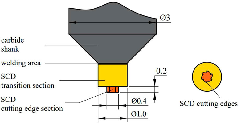
FIGURE 1. Structure of microscale multi-edge milling tool processed by picosecond laser.
2.2 Optimal pitch and machining width of laser cutting
The laser processing depth of cutting-edges and transition section is beyond the working range of picosecond laser (depth of field), so layered cutting is applied to laser machining process, which means that laser continuously focuses and ablates the surface formed by previous processing. The Gaussian distribution of laser energy makes the laser ablation remove the material unevenly. And when laser is irradiated on an uneven surface, the projection of circular laser spot on the ablated surface is irregular, which results in a great difference in the energy density of picosecond laser ablation in different regions. Using a laser processing path with a specific overlap ratio can obtain a relatively flat laser processed surface for subsequent laser ablation (Figure 2A).
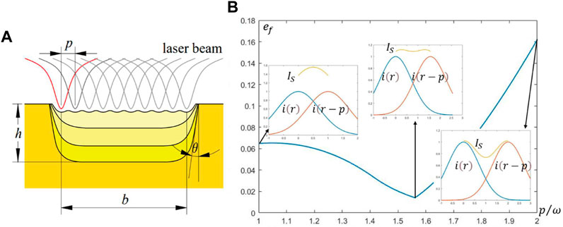
FIGURE 2. Effect of laser path overlap on the flatness of machined surface, (A) ablated surface formation process using laser layered cutting, (B) the influence of Gaussian laser beam overlaps on the fluctuation of accumulated energy.
The spatial distribution
Furthermore, the accumulated absorbed laser energy
Where,
The optimal pitch of laser processing paths
Although the bottom of the formed surface is relatively flat, the energy density of the laser on the inclined sidewall is greatly reduced, and possibly even less than the material removal threshold. Therefore, in layered cutting, the removal of bottom material will be much more obvious than that of side wall material. As the number of picosecond laser processing increases, steep side walls will be formed, which are not easy to be ablated. As shown in Figure 2A,
2.3 Laser processing path planning
SCD transition section is machined from 1 mm thick SCD sheet by layered cutting using a group of concentric circular picosecond laser processing paths. The minimum radius
After the cylindrical transition section is obtained, the lower surface is precisely removed by laser ablation, and the remaining material forms the cutting-edges. Based on such a processing strategy, the intuitive method is to process all cutting edges at one time with the profiled helix of the cutting section contour as the processing path (Figure 3A). In theory, the edge profile error of the processed milling tool only includes the positioning error of laser spot and the laser-induced defects, and the included angle between cutting-edges and tool profile can be guaranteed. However, the eccentricity between the laser processing path and the shank will destroy the radial runout of the cutting-edges in actual processing. In addition, the continuous laser processing causes the diamond to be heated continuously due to laser thermal effect, resulting in graphitization which seriously affects the cutting performance of the tools (Figure 3B).
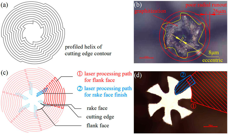
FIGURE 3. Two laser machining path for cutting section, (A) the profiled helix of the cutting-edge contour, (B) optical microscope image of cutting edges using (A) as processing path, (C) laser processing path of fractional array machining, (D) optical microscope image of cutting edges using (C) as processing path.
The profile accuracy and concentricity of the cutting-edges are important indicators to determine the cutting performance. Considering that the eccentricity between the laser processing path and the shank caused by its position error in the laser processing system is difficult to avoid, the processing path needs to be optimized so that the cutting-edge runout is not affected by the shank position. The fractional array machining will help to suppress the cutting-edge runout caused by the position error of the shank. In one process of laser ablation, only one cutting edge is processed, and then the same processing path is used to process another after the shank is rotated until all cutting edges are processed (Figure 3C). Using this processing strategy, the center of the circular array of the processing path is the axis of the shank. Therefore, the position error of the shank in the laser processing system only slightly affects the diameter of cutting section on milling tool, and does not affect the radial runout of the cutting-edges.
Due to the inertia of the optical element that controls laser spot position, the scanning speed of laser at the abrupt change-point of the processing path will be reduced, and the long-time stay of laser makes excessive material removal, as a result, it is not easy for laser beam machining to process sharp features. Considering that the cutting-edges need to be sharp enough to ensure good processing performance, the rake and flank face of the milling tool are processed separately and form the cutting edges to avoid the long-time stay of laser and obtain a fine cutting-edge profile. As shown in Figure 3C, the chip removal groove and the flank face are processed by the laser with the red processing path, and then the rake face is finished by the laser according to the blue processing path, and the cutting edge is formed.
3 Experimental verification
3.1 Laser machining system
The laser processing system is composed of picosecond laser, beam expander, galvanometer, f-θ lens, energy monitor and mechanical motion axis (Figure 4). The picosecond laser (Trumpf) can produce a laser with pulse width of 8 ps, maximum average power of 40 W, base frequency of 400 kHz and beam quality M2 of up to 1.1. The beam expander increases the aperture of the parallel light generated from the laser to facilitate the generation of higher quality laser spot. The mirror in the galvanometer controlled by computer can change the direction of laser propagation, and the high-speed moving mirror in the galvanometer can provide a maximum scanning speed of 3 m/s for the laser spot movement. The laser is focused on the plane about 100 mm below the f-θ lens, which has the maximum laser energy density and is used as the working plane of picosecond laser. The energy monitor in the optical path monitors the output power of the picosecond laser in real time and feeds it back to picosecond laser to provide the correct and stable energy of the laser output. The vertical straight axis (Z-axis) can change the position of the laser working plane, and ensure that the processed area is in the focal plane of the laser during the whole laser processing. There are also two linear axes in the plane to adjust the position of the workpiece in the laser processing system. The rotation axis (C-axis) under the f-θ lens is used as the indexing head to rotate the shank which was clamped on it with a self-centering fixture.
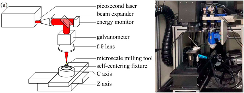
FIGURE 4. Picosecond laser machining system, (A) schematic diagram of optical path and motion axes, (B) picture during processing.
The diamond to be laser processed is a diamond sheet synthesized by means of high temperature and high pressure (HPHT), with thickness of 1.0 mm. The microscale milling tools with rake angle of 5°, 0°, −15°, −30° and clearance angle of 10° are processed by picosecond laser with average laser power of 4 W, scanning speed of 0.5 m/s and the predetermined processing path, and prepared for cutting performance testing.
3.2 Cutting performance test
The cutting test of the microscale milling tool is carried out on the precision 5-axis machining center Kern Micro. The milling tool produced by picosecond laser is installed on the milling spindle with the maximum rotational speed of 50000 rpm and radial runout of less than 0.8 μm by HSK tool holder. The linear feed axis of the machine tool is driven by a linear motor, which can realize the stable movement of low feed speed with positioning accuracy of 1 μm and repetitive positioning accuracy of 0.5 μm. The two rotation axes of the machine tool are B and C axes, with positioning accuracy of 0.002° and their axes are parallel to Y and Z-axes respectively (Figure 5). The workpiece used for milling tool cutting performance test is a 1 mm thick fused silica sheet with Mohs hardness of 7. The fused silica sheet is fixed on the force-measuring device installed in the machine tool through the clamp, which can detect and store the cutting force data of fused silica specimen in real time. In the milling experiment, each milling tool was used with spindle speed of 35000 rpm, cutting depth of 0.05 mm and three different feed rates of 5, 10 and 15 mm/min.
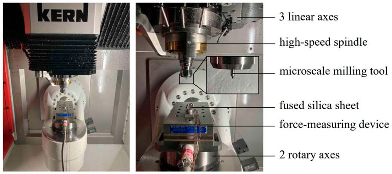
FIGURE 5. Experimental apparatus for cutting performance verification of SCD microscale milling tool.
4 Results and discussions
4.1 Cutting edges profile and graphitization of laser-processed diamond tools
The profile of SCD milling tool processed by direct machining strategy and fractional array machining strategy is measured and analyzed by optical microscope. Figure 3B shows the morphology of all cutting edges processed with direct machining strategy. Due to the continuous laser ablation for a long time, a large number of thermal defects including cracks and fragmentation appear on the diamond surface, the cutting edges are not sharp, and the profile of the cutting edge is seriously poor. The centers of the two concentric circles in Figure 3B are the axis positions of the cylindrical shank, and the two circles are the maximum and minimum rotation circles of the cutting edges, respectively. The radius difference between the two circles is defined as total radial runout of the cutting edges. The eccentricity between the geometric center of cutting edges and the shank axis is measured as 8 μm. Due to the position error of the shank in the laser processing system and serious laser-induced processing defects, the total radial runout of the six cutting edges is 26 μm. Such a large runout makes the cutting edges unable to fully participate in cutting and unstable actual feed per tooth will lead to poor processing effect of brittle materials.
In contrast, the microscale milling tool machined with fractional array processing strategy has significantly improved in terms of tool profile, cutting-edge sharpness and radial runout (Figure 6). The cutting edges with fine profile are evenly distributed, and the thermal crack is suppressed. The part of the diamond removed to get each cutting edge is marked in Figure 3C, including 6 chip removal grooves and 6 areas removed for rake face finishing. Since the fractional array machining effectively suppresses the cutting-edge runout caused by the position error of shank in laser processing, the total radial runout of cutting edges with different rake angles are 9.4 μm, 5.3 μm, 7.6 μm and 8.6 μm respectively. And the deviation of cutting section diameter is about 10 μm. The intersection of the rake faces and the flank faces form sharp cutting edges, and the radius of the edge is about 3.2 ± 2.1 μm. After laser processing of tools with theoretical rake angle of 5°, 0°, - 15° and - 30°, the actual rake angle is 6°, 0°, −16° and −29°, and the maximum error is approximately 1°. All cutting edges have a clearance angle of about 10°, which can effectively reduce the friction between the flank faces and the machined surface.
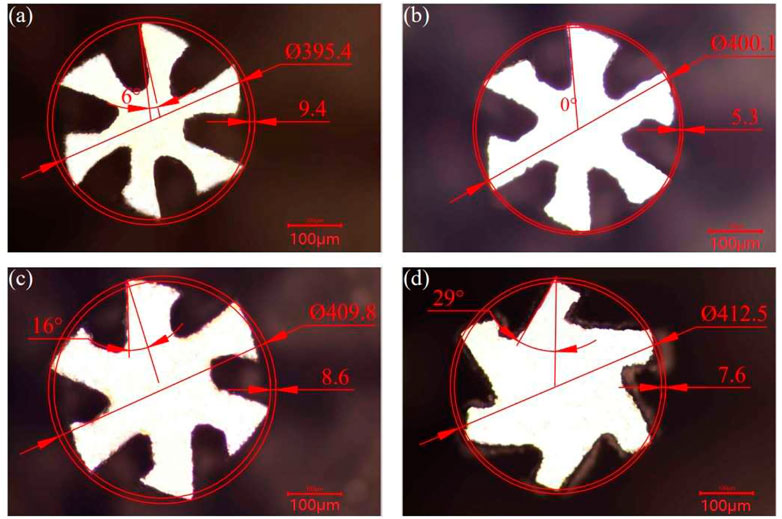
FIGURE 6. Optical microscope image of cutting edge profile for microscale milling tools with rake angle of (A) 5°, (B) 0°, (C) −15° and (D) −30°.
SCD is prone to graphitization at high temperature, and this change in atomic distribution will greatly damage the performance of diamond tools. In addition to the geometric characteristics of the tool, the graphitization of the tool surface needs to be monitored for the diamond tool made by laser. Considering that diamond and graphite have different characteristic peaks, Raman spectroscopy can analyze the graphitization degree of the SCD surface. Laser with wavelength of 633 nm and power of 17 mW was used as light source for Raman spectroscopic investigation. And the measuring position was the side edge of the milling tool, which has the longest laser ablation time and has an important impact on the cutting performance.
The Raman shift peaks at 1,333 cm-1 (
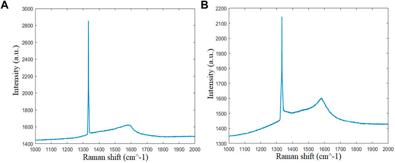
FIGURE 7. Raman spectrum of diamond milling tools machined with two laser processing paths, (A) the profiled helix of the cutting-edge contour, (B) fractional array machining.
4.2 Micro milling of fused silica using laser shaped tools
To demonstrate the cutting performance of laser shaped tools, micro-milling tests on fused silica were conducted under different cutting conditions. The effects of rake angle on cutting force and the degree of brittle damage on the subsurface of fused silica are studied. After machining, the machined fused silica surfaces are observed by optical microscope and scanning electron microscope (SEM, Tescan). The SEM image of Figure 8B indicate that the machined surface of fused silica is not smooth, but has sub-micron to micron size crushing without obvious cracks. The cutting force of micro-milling was also monitored and recorded in real time. The result shows that the amplitude of cutting force is stable and no tool fracture occurs. The cutting force increases slightly when the cutting tool with negative rake angle is used. Table1 shows the amplitude of cutting force using different rake angles and feed rates. Cutting force is mainly affected by the feed rate. In the cutting performance experiment, the cutting force is basically proportional to the feed rate.
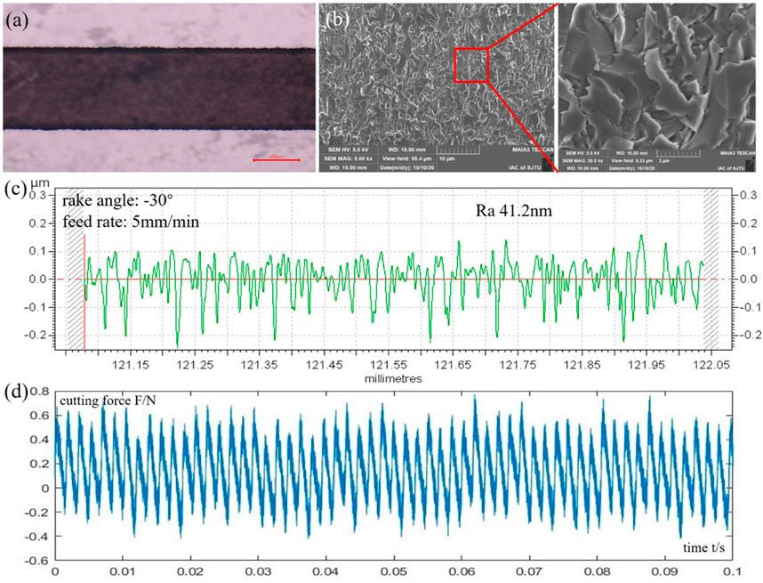
FIGURE 8. Cutting performance of SCD microscale milling tool with rake angle of −30° (ap = 0.05 mm, f = 0.143 μm/rev), (A) optical microscope image of groove, (B) SEM image of fused silica machined surface, (C) surface roughness Ra of fused silica machined surface, (D) cutting force monitor of micro-milling process.

TABLE 1. Amplitude of cutting force in relation to rake angle and feed rate.
Figure 9 shows the test result of roughness Ra obtained with surface profile instrument. The experimental results show that the fused silica processed with the negative rake angle tool has lower surface roughness, and the negative rake angle tool is suitable for milling process of fused silica. Moreover, a more obvious negative rake angle can produce a surface with lower roughness, under the conditions of all feed rates in the cutting experiment. When the feed rates are 5 mm/min and 10 mm/min, the milling tool with rake angle of 5° has better cutting performance than the tool with 0° rake angle at the beginning of milling, but the sharp wear of the positive rake angle tool when machining hard and brittle materials causes the rapid deterioration of the cutting-edge state, making its service life very short.
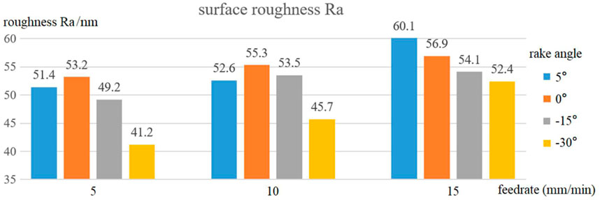
FIGURE 9. Effect of rake angle on machined surface roughness of fused silica under three feed rates in micro-milling.
In addition, for the same tool, the surface roughness of the machined surface increases with the increase of feed speed. When using the SCD milling tool with a rake angle of −30°, the surface damage of fused silica samples is the least. For the hard and brittle material such as fused silica, the tool with negative rake angle can help to suppress the formation of cracks and has the advantage of obtaining a surface with low roughness. Even though the SCD milling tool made by laser does not achieve the plastic removal of fused silica, the machined surface of fused silica with roughness Ra of 41.2 nm is obtained using the SCD milling tool with rake angle of −30°, cutting depth of 0.05 mm and feed rate of 0.143 μm/rev (Figure 8C).
4.3 The regression of tool cutting performance and tool life
After continuous milling of fused silica with laser-machined SCD microscale milling tool for 22 min (ap = 0.05 mm, f = 0.143 μm/rev), the machined surface roughness Ra has increased from 44 nm to 67 nm. Tool wear was evaluated by SEM image (Figure 10A). It is found that the tool wear mainly occurred at the rake face near the bottom edge and the side edge, in terms of chipping of the tool tip and the flaky peeling of rake face. According to the diameter of tool cutting section, continuous working time and spindle speed, the maximum cutting length of the tool tip on diamond milling tool with rake angle of −30° can be estimated as 967.6 m when used for fused silica milling with cutting depth of 0.05 mm and feed per revolution of 0.143 μm. Such microscale tool life can ensure that the machining of micro-structure with small machining range can be completed without switching tools.
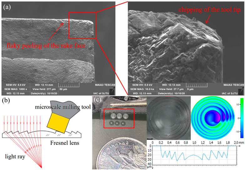
FIGURE 10. SCD milling tool after being used and a processing application, (A) SEM image of micro milling tool wear, (B) micro milling strategy for Fresnel lens, (C) microscale Fresnel lens array machined by laser-produced SCD milling tool and its profile.
In order to further verify the processing ability of laser processed SCD milling tool on the microstructure surface of fused silica, a microscale Fresnel lens array was processed on the optical fused silica surface. The optical refraction surface of the Fresnel lens was processed by the bottom edge of the microscale milling tool, and the non-working surface of the Fresnel lens was processed by the side edge. (Figure 10B). The specific milling tool orientation and tool center position were calculated by the normal direction of the Fresnel lens surface and the machining process was carried out on the CNC five-axis machining center. As shown in Figure 10 c, three Fresnel lenses with aperture of 1.6 mm and focal length of 8 mm were completed with a laser-processed diamond milling tool with negative rake angle of −30°. Figure 10C shows the optical microscope image of one Fresnel lens and its cross-section measured by surface profile instrument. The bright and clear focus spot indicate that the processed Fresnel lens has high-precision profile and good surface finish.
5 Conclusion
In this work, a picosecond laser based single crystal diamond tool fabrication technology is proposed to generate micro milling tools. A series of experimental tests have been carried out to investigate the feasibility of using picosecond laser in shaping SCD multi-edge microscale milling tool, optimal laser processing parameters, and the tool cutting performance under various cutting conditions. The conclusions are summarized as follows.
(1) Fractional array machining strategy for the multi-edge milling tools can effectively reduce the cutting-edge runout. Position error of shank affects diameter of cutting section slightly but not the total radial runout of cutting edges. A multi-edge milling tool with a minimum rotary diameter of 0.4 mm has been obtained.
(2) Cutting force is approximately proportional to the feed rate, and the rake angle of milling tool has little effect on it. The use of milling tool with negative rake angle is conducive to machining a low roughness surface of fused silica.
(3) A Fresnel lens array on the surface of fused silica was successfully generated by laser-machined SCD microscale milling tool, which verified that the tool prepared by laser can manufacture optical microstructures.
Data availability statement
The original contributions presented in the study are included in the article/supplementary material, further inquiries can be directed to the corresponding author.
Author contributions
JS—study, experiment, article writing ZT—participate in the study, article writing ZY—support and funding XJ—support and funding.
Acknowledgments
The authors acknowledge for the support from the National Natural Science Foundation of China under the Grant Nos. U20A20284 and 52075323.
Conflict of interest
The authors declare that the research was conducted in the absence of any commercial or financial relationships that could be construed as a potential conflict of interest.
Publisher’s note
All claims expressed in this article are solely those of the authors and do not necessarily represent those of their affiliated organizations, or those of the publisher, the editors and the reviewers. Any product that may be evaluated in this article, or claim that may be made by its manufacturer, is not guaranteed or endorsed by the publisher.
References
Aurich, J. C., Reichenbach, I., and Schuler, G. M. (2012). Manufacture and application of ultra-small micro end mills. CIRP Ann. Manuf. Technol. 61, 83–86. doi:10.1016/j.cirp.2012.03.012
Bartolo, P., Kruth, J-P., Silva, J., Levy, G., Malshe, A., Rajurkar, K., et al. (2012). Biomedical production of implants by additive electro-chemical and physical processes. CIRP Ann. Manuf. Technol. 61, 635–655. doi:10.1016/j.cirp.2012.05.005
Chae, J., Park, S. S., and Freiheit, T. (2006). Investigation of micro cutting operations. Int. J. Mach. Tools Manuf. 46, 313–332. doi:10.1016/j.ijmachtools.2005.05.015
Chen, Li, Piao, Yinchuan, Zhang, Feihu, Zhang, Yong, Hu, Y., and Wang, Y. (2022). Understand anisotropy dependence of damage evolution and material removal during nanoscratch of MgF2 single crystals. Int. J. Extrem Manuf. 5, 015101. doi:10.1088/2631-7990/ac9eed
Eberle, G., Dold, C., and Wegener, K. (2015). Laser fabrication of diamond micro-cutting tool-related geometries using a high-numerical aperture micro-scanning system. Int. J. Adv. Manuf. Technol. 81 (5-8), 1117–1125. doi:10.1007/s00170-015-7240-x
Geng, Z., Tong, Z., Huang, G., Zhong, W., Cui, C., Xu, X., et al. (2022). Micro-grooving of brittle materials using textured diamond grinding wheels shaped by an integrated nanosecond lasersystem. Int. J. Adv. Manuf. Technol. 1, 5389–5399. doi:10.1007/s00170-022-08695-2
Holmberg, S., Perebikovsky, A., Kulinsky, L., and Madou, M. (2014). 3-D micro and nano technologies for improvements in electrochemical power devices. Micromachines. 5, 171–203. doi:10.3390/mi5020171
Hsu, E. M., Mailman, N. A., Botton, G. A., and Haugen, H. K. (2011). Microscopic investigation of single-crystal diamond following ultrafast laser irradiation. Appl. Phys. A 103 (1), 185–192. doi:10.1007/s00339-010-5986-4
Kim, Jaegu, Tae-Jin, Je, Cho, Sung-Hak, Eun-Chae, Jeon, and Kyung-Hyun, Whang (2014). Micro-cutting with diamond tool micro-patterned by femtosecond laser. Int. J. P. R. Eng. Man. 15 (6), 1081–1085. doi:10.1007/s12541-014-0440-8
Konov, Vitaly I. (2012). Laser in micro and nanoprocessing of diamond materials. Laser Photonics Rev. 6 (6), 739–766. doi:10.1002/lpor.201100030
Kumar, Sumit, Tong, Zhen, and Jiang, Xiangqian (2022). Advances in the design and manufacturing of novel freeform optics. Int. J. Extrem Manuf. 4, 032004. doi:10.1088/2631-7990/ac7617
Malayath, Ganesh, Sidpara, Ajay M., and Deb, Sankha (2020). Fabrication of micro-end mill tool by EDM and its performance evaluation. Mach. Sci. Technol. 24 (2), 169–194. doi:10.1080/10910344.2019.1636269
Mao, S. S., Quéré, F., Guizard, S., Mao, X., Russo, R., Petite, G., et al. (2004). Dynamics of femtosecond laser interactions with dielectrics. Appl. Phys. A 79 (9), 1695–1709. doi:10.1007/s00339-004-2684-0
Meng, F., Zhou, R., Davis, T., Cao, J., Wang, Q. J., Hua, D., et al. (2010). Study on effect of dimples on friction of parallel surfaces under different sliding conditions. Appl. Surf. Sci. 256 (9), 2863–2875. doi:10.1016/j.apsusc.2009.11.041
Mouhamadali, F., Equis, S., Saeidi, F., Best, J. P., Cantoni, M., Hoffmann, P., et al. (2020). Nanosecond pulsed laser-processing of CVD diamond. Opt. Lasers Eng. 126, 105917. doi:10.1016/j.optlaseng.2019.105917
Nan Lia, Hao, Xie, Ke Ge, Wu, Bo, and Zhu, Wei Qiang (2020). Generation of textured diamond abrasive tools by continuous-wave CO2 laser: Laser parameter effects and optimisation. J. Mater Process Technol. 275, 116279. doi:10.1016/j.jmatprotec.2019.116279
Okamoto, Yasuhiro, Okubo, Tubasa, Kajitani, Atsuya, and Okada, Akira (2022). High-quality micro-shape fabrication of monocrystalline diamond by nanosecond pulsed laser and acid cleaning. Int. J. Extrem Manuf. 4, 025301. doi:10.1088/2631-7990/ac5a6a
Pettersson, U., and Jacobson, S. (2006). Tribological texturing of steel surfaces with a novel diamond embossing tool technique. Tribol. Int. 39 (7), 695–700. doi:10.1016/j.triboint.2005.06.004
Shinoda, M., Gattass, R. R., and Mazur, E. (2009). Femtosecond laser-induced formation of nanometer-width grooves on synthetic single-crystal diamond surfaces. J. Appl. Phys. 105 (5), 053102. doi:10.1063/1.3079512
Tong, Zhen, Luo, Xichun, Sun, Jining, Liang, Yingchun, and Jiang, Xiangqian (2015). Investigation of a scale-up manufacturing approach for nanostructures by using a nanoscale multi-tip diamond tool. Int. J. Adv. Manuf. Technol. 80, 699–710. doi:10.1007/s00170-015-7051-0
Wang, Fei, Shan, Chao, Yan, Jian-ping, Fu, Jiao, Garuma Abdisa, D., Zhu, T. f., et al. (2016). Application of femtosecond laser technique in single crystal diamond film separation. Diam. Relat. Mater 63, 69–74. doi:10.1016/j.diamond.2015.11.015
Wu, Mingtao, Guo, Bing, Zhao, Qingliang, He, Ping, Zeng, Z., and Zang, J. (2018). The influence of the ionization regime on femtosecond laser beam machining mono-crystalline diamond. Opt. Laser Technol. 106, 34–39. doi:10.1016/j.optlastec.2018.03.031
Wu, Xian, Liang, Li, Ning, He, Zhao, Guolong, and Jiang, Feng (2019). Fabrication of PCD micro end mill for machining hard and brittle material. Int. J. Adv. Manuf. Technol. 103, 1349–1358. doi:10.1007/s00170-019-03343-8
Xu, Z. W., Fang, F. Z., Zhang, S. J., Zhang, X. D., Hu, X. T., Fu, Y. Q., et al. (2010). Fabrication of micro DOE using micro tools shaped with focused ion beam. Opt. Express 18 (8), 8025–8032. doi:10.1364/oe.18.008025
Zhao, Yu, Liu, Huagang, Yu, Tianbiao, and Hong, Minghui (2021). Fabrication of high hardness microarray diamond tools by femtosecond laser ablation. Opt. Laser Technol. 140, 107014. doi:10.1016/j.optlastec.2021.107014
Keywords: micro-milling tool, picosecond laser, fused silica, damage layer, structured surface
Citation: Song J, Tong Z, Yao Z and Jiang X (2023) Micro milling of fused silica using picosecond laser shaped single crystal diamond tools. Front. Mater. 10:1176545. doi: 10.3389/fmats.2023.1176545
Received: 28 February 2023; Accepted: 03 April 2023;
Published: 12 May 2023.
Edited by:
Shiv Prakash Singh, International Advanced Research Center for Powder Metallurgy and New Materials (ARCI), IndiaReviewed by:
Bernhard Karpuschewski, Stiftung Institut für Werkstofftechnik, GermanyChen Li, Harbin Institute of Technology, China
Yebing Tian, Shandong University of Technology, China
Copyright © 2023 Song, Tong, Yao and Jiang. This is an open-access article distributed under the terms of the Creative Commons Attribution License (CC BY). The use, distribution or reproduction in other forums is permitted, provided the original author(s) and the copyright owner(s) are credited and that the original publication in this journal is cited, in accordance with accepted academic practice. No use, distribution or reproduction is permitted which does not comply with these terms.
*Correspondence: Zhenqiang Yao, enF5YW9Ac2p0dS5lZHUuY24=