 Kwang Jae Lee1
 Xinyi Wen1
 Yusuke Nakazato1
 Jaeyi Chun1
 Maliha Noshin1Chuanzhe Meng1,2
 Srabanti Chowdhury1*
- 1Department of Electrical Engineering, Stanford University, Stanford, CA, United States
- 2Department of Materials Science and Engineering, Stanford University, Stanford, CA, United States
Embedding p-type gallium nitride (p-GaN) in AlxGa1-xN-based thin films has garnered significant interest as a versatile structure for bandgap engineering such as tunnel/super-junctions or current blocking/guiding functions in electronic devices. However, Mg, a p-GaN dopant, has an undesirable diffusive capacity into the nearby thin films at a high growth temperature (>1,000°C), resulting in structural challenges in device design. This study systematically investigated the low-temperature GaN (LT-GaN) layer regrown on p-GaN that suppresses Mg diffusion according to metal–organic chemical vapor deposition growth conditions. Prototype Al0.3Ga0.7N (40 nm)/GaN (140 nm) high-electron-mobility transistors (HEMTs) were regrown with LT-GaN on p-GaN (300 nm), and a high two-dimensional electron gas (2DEG) density of 3.13E12 cm−2 was achieved by inserting a 100-nm-thick LT-GaN layer grown at 750°C; in contrast, only 1.76E10 cm−2 2DEG density was obtained from Al0.3Ga0.7N/GaN HEMTs regrown directly on p-GaN (Mg: 4.0E19 cm−3). The fabricated Al0.3Ga0.7N/GaN HEMTs with 100-nm-thick LT-GaN demonstrated a high drain current density of 84.5 mA/mm with a low on-state resistance of 31 Ω·mm. The AlxGa1-xN/LT-GaN/p-GaN platform demonstrated here paves the way for various III-nitride-based structures with embedded p-GaN.
1 Introduction
Gallium nitride (GaN) has attracted a great deal of attention as a next-generation power electronic material to replace silicon (Si) due to its excellent characteristics such as high electron mobility and high breakdown field (Chowdhury et al., 2013; Chowdhury and Mishra, 2013). In general, GaN thin films are grown using a metal–organic chemical vapor deposition (MOCVD) system, and Mg doping for p-type GaN (p-GaN) remains as a last step on the top of epitaxial layers due to the large diffusivity of Mg from the p-GaN surface and the reactor wall of MOCVD (Ran et al., 2006). Evidently for the Ga-polar p-GaN thin-film growth (Benzarti et al., 2008), these residual Mg dopants unintentionally diffuse into AlxGa1-xN-based thin films that are regrown on p-GaN, even though Mg source (Cp2Mg) injection into a reactor was ceased (Fichtenbaum et al., 2008). Nevertheless, embedding p-GaN has recently emerged as an important research topic to create more efficient and higher-performance electronic devices, e.g., lateral AlGaN/GaN high-electron-mobility transistors (HEMTs) including a p-GaN buffer layer (Lee et al., 2014), vertical super-junction metal-oxide-semiconductor field-effect transistors (MOSFETs) using a field-stop p-GaN layer (Xiao et al., 2019; Zhou et al., 2019), and current aperture vertical electron transistors (CAVETs) with a current blocking p-GaN layer (Chowdhury et al., 2008; 2011).
To date, various solutions have been suggested to suppress Mg out-diffusion such as ex situ wet chemical treatment using hydrofluoric acid (Xing et al., 2003), the in situ dry etching process with H2 carrier gas (Soman et al., 2019), alternative regrowth using molecular beam epitaxy (MBE) instead of using MOCVD (Chowdhury et al., 2011; Brown et al., 2013; Wu et al., 2021), and the introduction of low-temperature aluminum nitride (LT-AlN) or LT-GaN insertion layers as an Mg suppression layer (MSL) (Tomita et al., 2008; Agarwal et al., 2017). Agarwal et al. (2017) recently reported the LT flow-modulated epitaxy (referred to as pulsed LT-GaN) technique for high crystallinity of intrinsic GaN (i-GaN) regrown on p-GaN with improved surface morphology as well as suppression of Mg out-diffusion. As the demand for embedding p-GaN in the AlxGa1-xN thin film without Mg diffusion increases explosively, it is also important to explore the characteristics of MSLs through an electronic device embedding p-GaN.
In this study, we systematically investigate the efficacy of LT-GaN regrown on p-GaN as the MSL and its dependence on MOCVD growth conditions. Two types of MSL with and without perturbation (or pulsed injection) of a trimethylgallium (TMGa) metal–organic source were employed to investigate Mg out-diffusion: (1) an MSL with a continuous injection (CLT-GaN) and (2) an MSL with a pulsed injection (PLT-GaN) of the TMGa source. Subsequently, Al0.3Ga0.7N (40 nm)/i-GaN (140 nm) thin films for prototype HEMTs were regrown on MSLs to explore the decay rate of Mg diffusion and the two-dimensional electron gas (2DEG) characteristics. Secondary ion mass spectrometry (SIMS) depth profiles were measured to analyze the Mg diffusion into regrown Al0.3Ga0.7N/i-GaN according to the MOCVD growth condition of LT-GaNs. Capacitance–voltage (C–V) and current–voltage (I–V) measurements were also taken to understand 2DEG and the output/transfer characteristics of Al0.3Ga0.7N/i-GaN HEMTs with our LT-GaN MSLs. This work demonstrates the importance of suppressing Mg out-diffusion in device performance and shows the correlation between the degree of Mg diffusion and 2DEG density according to various growth conditions of existing LT-GaN.
2 Experimental procedure
A 300-nm-thick p-GaN and 3 µm-thick i-GaN buffer layer were grown at 930°C and 1,040°C, respectively, by using the MOCVD system. The Al0.3Ga0.7N (40 nm)/i-GaN (140 nm) thin films including the MSL were regrown with the ex situ process for the HEMTs. There were two types of samples grown in this study, as shown in Supplementary Figure S1: (A) HEMT structures on a sapphire substrate with various LT-GaN techniques for the C–V measurement using a Hg-probe tool and (B) the same structures on a GaN substrate for the device characteristics of lateral HEMTs. Figure 1A shows a schematic illustration of Al0.3Ga0.7N/i-GaN with LT-GaN MSLs regrown on the p-GaN layer. First, two p-GaNs with different Mg doping concentrations (1.0E19 and 4.0E19 cm−3) were grown on sapphire substrates. After that, two types of the MSL, CLT-GaN and PLT-GaN, were introduced to investigate Mg out-diffusion from p-GaN. The CLT-GaN MSL was regrown under a growth pressure of 600 mbar at 750°C with a consistent flow rate of TMGa and NH3 sources into a H2 atmospheric MOCVD reactor. Meanwhile, 50 cycles of (i) TMGa interruption (5 s) and (ii) TMGa injection (3 s) were implemented for the PLT-GaN MSL at the same growth pressure and temperature as the CLT-GaN MSL. Figure 1B shows the in situ reflectance and growth temperature during the MOCVD process for the Al0.3Ga0.7N/i-GaN/PLT-GaN thin-film regrowth on p-GaN. The part of the PLT-GaN growth step in Figure 2B is shown enlarged in Figure 1C, where two different growth rates repeated 50 times in one cycle can be observed: (i) a TMGa interruption step (5 s) and (ii) a TMGa injection step (3 s). On the other hand, the growth behavior of CLT-GaN is continuous. To investigate the suppression of Mg out-diffusion by applying these LT-GaN MSLs, the MOCVD growth temperature and thickness of LT-GaN were controlled as summarized in Table 1. Subsequent regrowth was conducted for 140-nm-thick i-GaN and 40-nm-thick Al0.3Ga0.7N at 1,025°C and 1,080°C, respectively, to form the 2DEG structure. An XRD 2theta-omega scan of samples was performed, as shown in Supplementary Figure S6. For device fabrication, the mesa etching was performed using a dry etching process with inductively coupled plasma reactive ion etching (ICP-RIE). For the source electrodes, Ti, Al, Ni, and Au were deposited on Al0.3Ga0.7N followed by post-annealing using a rapid thermal annealing (RTA) system at 850°C for 45 s to form ohmic contacts. Al2O3 (12 nm thick) was deposited as a gate dielectric through atomic layer deposition (ALD). Ni/Au was deposited for the formation of the gate contact.
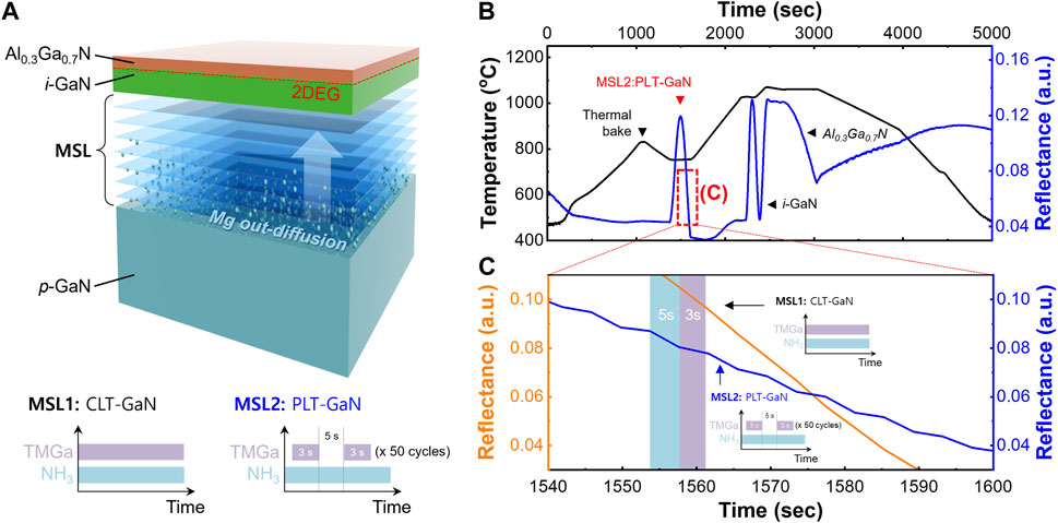
FIGURE 1. (A) Schematic structure of Al0.3Ga0.7N/i-GaN with LT-GaN MSLs regrown on p-GaN. Two types of the MSLs with and without perturbation (or pulsed injection) of a TMGa metal–organic source were introduced: the TMGa source for the MSL growth was injected in a continuous form (CLT-GaN) or a pulsed form (PLT-GaN). (B) In situ reflectance and growth temperature during the MOCVD process for Al0.3Ga0.7N/i-GaN/PLT-GaN thin-film regrowth. (C) The part of the PLT-GaN growth step in Figure 2B is shown enlarged, where two different growth rates repeated 50 times can be observed in one cycle: (i) TMGa interruption step (5 s) and (ii) TMGa injection step (3 s).
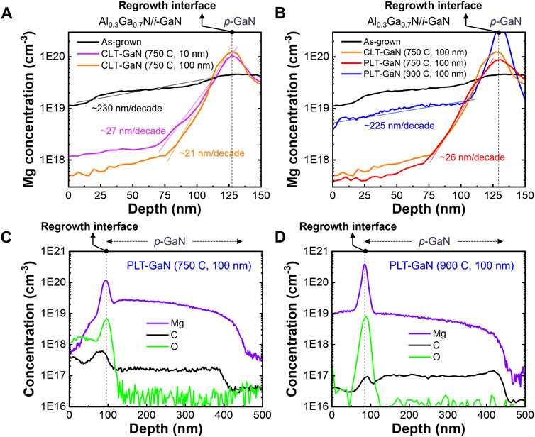
FIGURE 2. SIMS depth profiles to evaluate Mg out-diffusion decay rates in Al0.3Ga0.7N/i-GaN. (A) Thickness dependency of the CLT-GaN MSL. (B) Temperature dependency of the PLT-GaN MSL and SIMS depth profiles of Mg, C, and O for the 100-nm-thick PLT-GaN regrown at (C) 750°C and (D) 900°C. The fitting lines for extracting the Mg suppression rate are overlapped with the actual SIMS results.
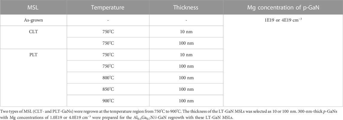
TABLE 1. MOCVD growth conditions for LT-GaN MSLs.
3 Results and discussion
Supplementary Figure S2 shows the AFM images of the grown 2DEG channel layer on sapphire substrates. RMS roughness shows significant differences between CLT- (∼1.4 nm) and PLT LT-GaN (∼0.40 nm). Figure 2 shows the SIMS depth profile for the regrown Al0.3Ga0.7N/i-GaN to evaluate Mg out-diffusion. The black dotted lines in Figure 2 indicate the p-GaN borderline or the place where the regrowth of Al0.3Ga0.7N/i-GaN with the MSL starts. The fitting lines for extracting the Mg suppression rate are overlapped with the actual SIMS results. For the as-grown sample without MSL (Figure 2A), the decay rate of Mg diffusion in the regrown Al0.3Ga0.7N/i-GaN region was estimated to be ∼230 nm/decade. This result generally shows the diffusivity of Mg into regrown thin films on p-GaN. On the other hand, 10-nm-thick CLT-GaN as an MSL dramatically reduces the Mg diffusion rate (∼27 nm/decade) in a regrown film. It was also found that CLT-GaN with a thickness of 100 nm further reduces Mg diffusion to ∼21 nm/decade. The lowest Mg concentrations at 150-nm thicknesses of the regrown Al0.3Ga0.7N/i-GaN layer were 6.69E18 cm−3 for as-grown, 9.75E17 cm−3 for 10-nm-thick CLT-GaN grown at 750°C, and 5.94E17 cm−-3 for 100-nm-thick CLT-GaN grown at 750°C. As Agarwal et al. (2017) previously reported, the PLT-GaN MSL regrown on p-GaN not only improves surface morphology but also suppresses Mg out-diffusion. Figure 2B shows that the 100-nm-thick PLT-GaN MSL grown at 750°C has a similar Mg suppression rate (∼26 nm/decade) compared to the CLT-GaN MSL under the same growth conditions, but the lowest Mg concentration at 150 nm is reduced by almost half (3.67E17 cm−3). Generally, these LT growth methods introduce various crystallography defects as well as impurities (C, O, and H) from byproducts of organic sources. The regrowth at a temperature lower than 750°C showed poor crystallinity of the thin films (not shown in this study) regardless of Mg suppression. For the other case, when the growth temperature is increased from 750°C to 900°C, 100-nm-thick PLT-GaN loses most of its role as the MSL, which indicates that Mg diffusion is very sensitive to the p-GaN surface temperature. Additionally, SIMS measurements, as shown in Figures 2C, D, obviously displayed the influence of growth temperature for the LT-GaN MSLs on the impurity concentration and the suppression of Mg diffusion. The concentration of O and C in the regrown Al0.3Ga0.7N/i-GaN layer decreases by more than one order of magnitude as the growth temperature of the MSL increases up to 900°C, but the suppression of Mg diffusion is significantly reduced. Since the impurity level strongly depends on the growth temperature, the impurities contained when inserting CLT-GaN and PLT-GaN grown at the same temperature are similar. Because of this reciprocal relationship, further studies on the LT-GaN MSL are required to simultaneously achieve Mg diffusion suppression and impurity reduction.
To investigate the 2DEG characteristics of regrown Al0.3Ga0.7N/i-GaN, the C–V measurement was obtained, as shown in Figure 3. Figure 3A shows the simulated energy band diagram of our Al0.3Ga0.7N/i-GaN. Bandgaps and offset values were obtained by the Silvaco TCAD (Sharbati et al., 2021). The calculated ΔEc and ΔEv were 377 and 171 meV, respectively. As shown in Figure 3B, the C–V measurements were directly obtained from the unprocessed samples at 1 MHz using a mercury (Hg)-probe system (MDC Model 802), which is commonly used for the C–V characterization of HEMTs without device fabrication (Cordier et al., 2008; Tucker et al., 2022). The Hg C–V system provides a non-destructive electrical characterization and employs a unique dot-ring configuration by forming a Schottky contact (dot contact) and an ohmic contact (ring contact) with the non-metalized planar semiconductor surface (Enisherlova et al., 2008). The C–V profiles show the measured capacitance with the bias voltage on the Schottky contact swept from 1 to −10 V, and the 2DEG sheet carrier density is calculated using the following equation (Kakanakova-Georgieva et al., 2007):
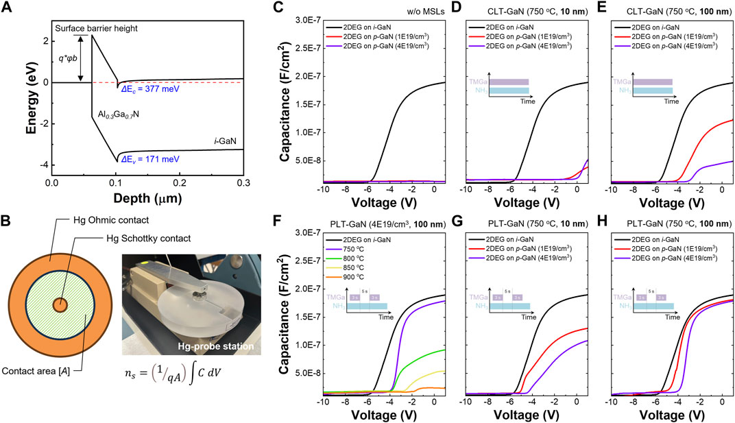
FIGURE 3. (A) Energy band diagram of our Al0.3Ga0.7N/i-GaN. (B) Photograph of the contactless Hg-probe station with schematics of a contact area for the measurement of 2DEG density. (C–H) C–V results of Al0.3Ga0.7N/i-GaN regrown on p-GaN with various MOCVD growth conditions of MSLs. The 2DEG density was extracted from the C–V curves.
Figure 4 presents the output and transfer characteristics of the fabricated lateral HEMTs regrown on p-GaN with 10- and 100-nm-thick PLT-GaN MSLs. Figure 4A shows the cross-section device schematics and the plan-view optical microscope image. In the case of HEMTs without the MSL, no 2DEG characteristics were observed (not shown). The gate voltage was swept from 0 to −4 in −1 V steps. The threshold voltage (Vth) was defined as the gate voltage (VG) when the drain current reaches 1 mA/mm at a drain bias of 5 V from the ID–VGS curve (Hwang et al., 2013). The on-state resistance is extracted from the gradient of ID–VDS curves at VGS = 0 V and VDS from 0 to 0.5 V. A maximum drain current density (Imax) increases from 41.5 to 84.5 mA/mm as the thickness of the PLT-GaN MSL increases, as shown in Figures 4B, C. The ID–VGS hysteresis was 0.21 and 0.14 V for the 10-nm- and 100-nm-thick MSL, respectively. From the SIMS and C–V analysis, it is shown that increasing the thickness of PLT-GaN MSLs could further suppress the Mg diffusion into the 2DEG. Therefore, Imax can be increased by maintaining a high-electron density in the 2DEG region. The Vth of these HEMTs is −4.12 V, and the on-state resistance is 52 and 31 mΩ∙mm with 10- and 100-nm-thick PLT-GaN, respectively. The ID–VGS transfer characteristics show well-behaved curves, as plotted in Figures 4D, E. The average gate leakage (IG) of HEMTs using 10- and 100-nm-thick PLT-GaNs was similar to ∼1.45E-8 A/mm. The ID off-current representing the leakage current characteristics related to defects was 5.74E-11 and 5.36E-11 A/mm, respectively, in the case of using 10- and 100-nm-thick PLT-GaNs. The two values do not show a large difference, and when PLT is used, defect density, one of the main issues of LT-GaN growth, shows no sensitivity according to the thickness of PLT-GaN. The subthreshold slopes were also calculated as 99.23 and 83.19 mV/dec for the 10- and 100-nm-thick MSLs, respectively.
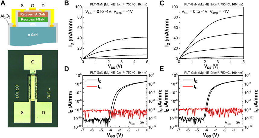
FIGURE 4. (A) Cross-section schematics and the plan-view optical microscope image of the lateral HEMT. ID–VDS measurement of lateral HEMTs on p-GaN using (B) 10-nm-thick and (C) 100-nm-thick PLT-GaNs as the MSL. Transfer characteristics of lateral HEMTs on p-GaN using (D) 10-nm-thick and (E) 100-nm-thick PLT-GaNs as the MSL.
4 Conclusion
We addressed the PLT-GaN and CLT-GaN inserted between Al0.3Ga0.7N/i-GaN and p-GaN to suppress Mg out-diffusion. In SIMS depth profiling, PLT-GaN improved the Mg decay rate up to ∼21 nm/decade in regrown Al0.3Ga0.7N/i-GaN on p-GaN, presenting a much higher decay rate compared to the case without any suppression layers (∼230 nm/decade). In addition, the C–V characteristic showed a high electron density of 3.13E12 cm−2 in 2DEG of Al0.3Ga0.7N/i-GaN with the PLT-GaN MSL on p-GaN (Mg: 4.0E19 cm−3), which is the almost same electron concentration (4.27E12 cm−2) as that in 2DEG grown without p-GaN. In addition, we successfully demonstrated the electrical characteristics of the lateral HEMTs regrown on p-GaN with 10- and 100-nm-thick PLT-GaN MSLs. This study provides a pathway to solve a critical bottleneck caused by Mg out-diffusion and enables diverse applications in high-efficiency and high-output power electronics that require GaN-based epi-structures embedding p-GaN layers.
Data availability statement
The raw data supporting the conclusion of this article will be made available by the authors, without undue reservation.
Author contributions
SC and KL designed and discussed the experiments. KL grew GaN-based thin films by using the MOCVD system. YN and JC designed the devices. XW, YN, and JC fabricated and analyzed the HEMT devices. KL and MN analyzed the SIMS results. CM analyzed C–V results. All authors contributed to the article and approved the submitted version.
Funding
The authors gratefully acknowledge the financial support provided by ONR grant N00014-21-1-2167, supervised by. Mr. (Ret. Capt.) Lynn Petersen.
Conflict of interest
The authors declare that the research was conducted in the absence of any commercial or financial relationships that could be construed as a potential conflict of interest.
Publisher’s note
All claims expressed in this article are solely those of the authors and do not necessarily represent those of their affiliated organizations, or those of the publisher, the editors, and the reviewers. Any product that may be evaluated in this article, or claim that may be made by its manufacturer, is not guaranteed or endorsed by the publisher.
Supplementary material
The Supplementary Material for this article can be found online at: https://www.frontiersin.org/articles/10.3389/fmats.2023.1229036/full#supplementary-material
References
Agarwal, A., Tahhan, M., Mates, T., Keller, S., and Mishra, U. (2017). Suppression of Mg propagation into subsequent layers grown by MOCVD. J. Appl. Phys. 121, 25106. doi:10.1063/1.4972031
Benzarti, Z., Halidou, I., Bougrioua, Z., Boufaden, T., and El Jani, B. (2008). Magnesium diffusion profile in GaN grown by MOVPE. J. Cryst. Growth 310, 3274–3277. doi:10.1016/j.jcrysgro.2008.04.008
Brown, D. F., Shinohara, K., Corrion, A. L., Chu, R., Williams, A., Wong, J. C., et al. (2013). High-speed, enhancement-mode GaN power switch with regrown ${\rm n}+ $ GaN ohmic contacts and staircase field plates. IEEE electron device Lett. 34, 1118–1120. doi:10.1109/led.2013.2273172
Chowdhury, S., and Mishra, U. K. (2013). Lateral and vertical transistors using the AlGaN/GaN heterostructure. IEEE Trans. Electron Devices 60, 3060–3066. doi:10.1109/ted.2013.2277893
Chowdhury, S., Swenson, B. L., and Mishra, U. K. (2008). Enhancement and depletion mode AlGaN/GaN CAVET with Mg-ion-implanted GaN as current blocking layer. IEEE Electron Device Lett. 29, 543–545. doi:10.1109/led.2008.922982
Chowdhury, S., Swenson, B. L., Wong, M. H., and Mishra, U. K. (2013). Current status and scope of gallium nitride-based vertical transistors for high-power electronics application. Semicond. Sci. Technol. 28, 074014. doi:10.1088/0268-1242/28/7/074014
Chowdhury, S., Wong, M. H., Swenson, B. L., and Mishra, U. K. (2011). CAVET on bulk GaN substrates achieved with MBE-regrown AlGaN/GaN layers to suppress dispersion. IEEE Electron Device Lett. 33, 41–43. doi:10.1109/led.2011.2173456
Cordier, Y., Moreno, J.-C., Baron, N., Frayssinet, E., Chenot, S., Damilano, B., et al. (2008). Demonstration of AlGaN/GaN high-electron-mobility transistors grown by molecular beam epitaxy on Si (110). IEEE electron device Lett. 29, 1187–1189. doi:10.1109/led.2008.2005211
Enisherlova, K. L., Gulyaev, I. B., Goryachev, V. G., Dorofeev, A. U., Temper, E. M., and Gladisheva, N. B. (2008). “AlxGa (1-x) N/GaN structure diagnostic by CV characteristics method,” in Micro-and nanoelectronics 2007 (Bellingham, Washington, USA: SPIE), 321–328.
Fichtenbaum, N. A., Mates, T. E., Keller, S., DenBaars, S. P., and Mishra, U. K. (2008). Impurity incorporation in heteroepitaxial N-face and Ga-face GaN films grown by metalorganic chemical vapor deposition. J. Cryst. Growth 310, 1124–1131. doi:10.1016/j.jcrysgro.2007.12.051
Hwang, I., Kim, J., Choi, H. S., Choi, H., Lee, J., Kim, K. Y., et al. (2013). p-GaN gate HEMTs with tungsten gate metal for high threshold voltage and low gate current. IEEE Electron Device Lett. 34, 202–204. doi:10.1109/led.2012.2230312
Kakanakova-Georgieva, A., Forsberg, U., Ivanov, I. G., and Janzén, E. (2007). Uniform hot-wall MOCVD epitaxial growth of 2 inch AlGaN/GaN HEMT structures. J. Cryst. Growth 300, 100–103. doi:10.1016/j.jcrysgro.2006.10.242
Lee, K. J., Nakazato, Y., Chun, J., Wen, X., Meng, C., Soman, R., et al. (2022). Nanoporous GaN on p-type GaN: a Mg out-diffusion compensation layer for heavily Mg-doped p-type GaN. Nanotechnology 33, 505704. doi:10.1088/1361-6528/ac91d7
Lee, Y.-J., Yao, Y.-C., Huang, C.-Y., Lin, T.-Y., Cheng, L.-L., Liu, C.-Y., et al. (2014). High breakdown voltage in AlGaN/GaN HEMTs using AlGaN/GaN/AlGaN quantum-well electron-blocking layers. Nanoscale Res. Lett. 9, 433–439. doi:10.1186/1556-276x-9-433
Ran, J., Wang, X., Hu, G., Wang, J., Li, J., Wang, C., et al. (2006). Study on Mg memory effect in npn type AlGaN/GaN HBT structures grown by MOCVD. Microelectron. J. 37, 583–585. doi:10.1016/j.mejo.2005.10.001
Sharbati, S., Gharibshahian, I., Ebel, T., Orouji, A. A., and Franke, W.-T. (2021). Analytical model for two-dimensional electron gas charge density in recessed-gate GaN high-electron-mobility transistors. J. Electron. Mater. 50, 3923–3929. doi:10.1007/s11664-021-08842-7
Soman, R., Raghavan, S., and Bhat, N. (2019). An in situ monitored and controlled etch process to suppress Mg memory effects in MOCVD GaN growth on Si substrate. Semicond. Sci. Technol. 34, 125011. doi:10.1088/1361-6641/ab5006
Tomita, K., Itoh, K., Ishiguro, O., Kachi, T., and Sawaki, N. (2008). Reduction of Mg segregation in a metalorganic vapor phase epitaxial grown GaN layer by a low-temperature AlN interlayer. J. Appl. Phys. 104, 14906. doi:10.1063/1.2952051
Tucker, E., Ramos, F., Frey, S., Hillard, R. J., Horváth, P., Zsákai, G., et al. (2022). Characterization of Al<i>X</i>Ga1−<i>X</i>N/GaN high electron mobility transistor structures with mercury probe capacitance–voltage and current–voltage. Phys. status solidi 219, 2100416. doi:10.1002/pssa.202100416
Wu, Y., Liu, B., Xu, F., Sang, Y., Tao, T., Xie, Z., et al. (2021). High-efficiency green micro-LEDs with GaN tunnel junctions grown hybrid by PA-MBE and MOCVD. Photonics Res. 9, 1683–1688. doi:10.1364/prj.424528
Xiao, M., Zhang, R., Dong, D., Wang, H., and Zhang, Y. (2019). Design and simulation of GaN superjunction transistors with 2-DEG channels and fin channels. IEEE J. Emerg. Sel. Top. Power Electron. 7, 1475–1484. doi:10.1109/jestpe.2019.2912978
Xing, H., Green, D. S., Yu, H., Mates, T., Kozodoy, P., Keller, S., et al. (2003). Memory effect and redistribution of Mg into sequentially regrown GaN layer by metalorganic chemical vapor deposition. Jpn. J. Appl. Phys. 42, 50–53. doi:10.1143/jjap.42.50
Keywords: pulsed low-temperature growth, Mg diffusion, MOCVD thin-film growth, AlGaN/GaN HEMT, power electronics
Citation: Lee KJ, Wen X, Nakazato Y, Chun J, Noshin M, Meng C and Chowdhury S (2023) A systematic study on the efficacy of low-temperature GaN regrown on p-GaN to suppress Mg out-diffusion. Front. Mater. 10:1229036. doi: 10.3389/fmats.2023.1229036
Received: 25 May 2023; Accepted: 16 November 2023;
Published: 05 December 2023.
Edited by:
Peide Ye, Purdue University, United StatesReviewed by:
Nicolò Zagni, University of Modena and Reggio Emilia, ItalyLakshmi Narayanan Mosur Saravana Murthy, Intel, United States
Copyright © 2023 Lee, Wen, Nakazato, Chun, Noshin, Meng and Chowdhury. This is an open-access article distributed under the terms of the Creative Commons Attribution License (CC BY). The use, distribution or reproduction in other forums is permitted, provided the original author(s) and the copyright owner(s) are credited and that the original publication in this journal is cited, in accordance with accepted academic practice. No use, distribution or reproduction is permitted which does not comply with these terms.
*Correspondence: Srabanti Chowdhury, c3JhYmFudGlAc3RhbmZvcmQuZWR1