 Shaoguang Zhao1
 Yu Zhao
 Li Tao
- 1Key Laboratory of Advanced Optoelectronic Quantum Architecture and Measurement (MOE), Centre for Quantum Physics, School of Physics, Beijing Institute of Technology, Beijing, China
- 2Guangdong Provincial Key Laboratory of Information Photonics Technology, Guangdong Provincial Key Laboratory of Functional Soft Condensed Matter, School of Material and Energy, Guangdong University of Technology, Guangzhou, China
In recent years, the use of 2D materials as surface-enhanced Raman scattering (SERS) active substrates has been extensively investigated. This mini review emphasizes the tunable interface characteristics of 2D materials as SERS substrates. Notably, 2D materials exhibit a wealth of tunable properties, encompassing energy levels, band structures, and interlayer coupling, which confer upon them significant potential as versatile SERS substrates. We summarize the recent advances in tunable 2D materials as SERS active substrates, providing guidance for future research in developing tunable multifunctional molecular sensors based on 2D materials.
Introduction
Raman spectroscopy was first discovered in 1928 (Raman and Krishnan, 1928). It relies on the interaction of light with the chemical bonds within a molecule, providing fingerprint information about molecular or lattice vibrations. This non-destructive molecular detection technique finds wide-ranging applications in various fields including chemical analysis, environmental protection, and food processing. However, because of the low Raman scattering cross-sections, the effectiveness of Raman spectroscopy is limited in detecting molecules with very low concentrations. Surface-enhanced Raman scattering (SERS) is a technique that can amplify the Raman signals of molecules on an active substrate, enabling even single-molecule detection. The generation of the SERS effect involves two primary enhancement mechanisms: electromagnetic mechanism (EM) and chemical mechanism (CM) (Campion and Kambhampati, 1998; Langer et al., 2020). The former achieves enhancement by utilizing surface plasma excitations to intensify the electromagnetic field on the SERS-active substrate, thus boosting the Raman signal intensity of molecules on the substrate surface (Schlücker, 2014). The latter relies on interactions between the SERS-active surfaces and molecules, such as charge transfer and exciton resonances. This interaction induces a modification in the electron density of the molecules, leading to heightened molecule polarization and thus amplified Raman scattering (Morton and Jensen, 2009; Lombardi and Birke, 2014).
The theory of EM has been extensively researched and demonstrated. In contrast, the understanding of CM remains largely limited to qualitative descriptions. The challenge lies in the fact that the Raman signal from chemical enhancement tends to be overshadowed by the Raman signal from electromagnetic enhancement, making it difficult to experimentally quantify the CM-induced Raman enhancement. In recent years, two-dimensional (2D) materials, such as graphene, hexagonal boron nitride, and transition metal dichalcogenides (TMDCs) such as MoS2, WSe2, and MoTe2, have demonstrated excellent SERS effects (Ling et al., 2014; Lee et al., 2016; Chen et al., 2020). Compared to noble metals, 2D materials possess atomic-level smooth surfaces, greater chemical stability, and exhibit stronger interactions with molecules. The primary mechanism by which 2D materials achieve SERS is considered to be CM, offering an ideal platform for understanding the CM mechanism in SERS. Moreover, because of unique properties such as the large surface-to-volume ratio and quantum confinement effect, 2D materials possess highly interface-tunable nature. Through precise modulation of the band structures and energy levels in 2D materials, optimized energy level alignment that facilitates the charge transfer and/or exciton resonances at the molecular-substrate interface can be achieved, culminating in a potent augmentation of the SERS effect. This tunability provides numerous avenues for the development of 2D materials as SERS-active substrates.
Herein, we present a comprehensive summary of recent research on achieving tunable SERS using 2D materials. We extensively discuss the capabilities of 2D material interface engineering in enhancing the performance of 2D materials as SERS-active substrates. This mini review serves as a guiding resource for the advancement of 2D materials as substrates for SERS applications and multifunctional optoelectronic sensing devices.
Electrostatic tunning
The tunable energy levels of 2D materials offer promising prospects for their application as tunable SERS-active substrates. Notably, monolayer graphene can be effectively manipulated by applying gate voltage to induce hole or electron doping, thus allowing precise control of its Fermi levels (Figure 1A) (Xu et al., 2011b). Negative gate voltage shifts the Fermi level of graphene downward, bringing the energy gap between the graphene Fermi level and the lowest unoccupied molecular orbital (LUMO) of the probe molecule closer to the incident laser excitation (1.96 eV). This significantly enhances the charge transfer resonance between probe molecules (Co-Pc) and the substrate, thereby enhancing the Raman signal of the probe molecules. Conversely, positive gate voltage weakens the charge transfer and leads to signal attenuation. Importantly, this modulation is reversible. In their subsequent work, the authors have further investigated the electrical tuning effects on SERS under different gas atmospheres (Xu et al., 2011a).
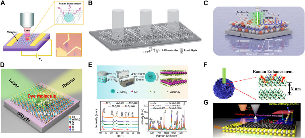
FIGURE 1. (A) Gate voltage-modulated SERS on graphene (Xu et al., 2011b). Copyright (2011) American Chemical Society. (B) Surface doping modulation of SERS on MoS2 (Sun et al., 2014). Copyright (2014) John Wiley & Sons. (C) Modulation of SERS on TMDC materials by alloy engineering (Tang et al., 2023). Copyright (2023) American Chemical Society. (D) Phase engineering to modulate the SERS on 2D transition metal tellurides (Tao et al., 2018). Copyright (2018) American Chemical Society. (E) Defect engineering for the modulation of MoS2-based SERS (Quan et al., 2022). Copyright (2022) John Wiley & Sons. (F) SERS effects on MoS2 modulated by interlayer coupling (Li et al., 2020). Copyright (2020) American Chemical Society. (G) Modulation of the SERS effect by the stacking order of van der Waals heterojunctions (Tan et al., 2017). Copyright (2017) American Chemical Society.
Furthermore, a comparative study was conducted between graphene field-effect doping and chemical doping (Hao et al., 2013). Both methods exhibited similar trends in terms of electron and hole doping, with p-doped graphene showing greater SERS enhancement compared to n-doped graphene.
The electrical tunning approach is expected to be suitable for semiconducting 2D materials. For instance, the SERS effect of tungsten oxide thin films can be electrically regulated (Zhou et al., 2019). The modulation of oxygen vacancy defects in WO3-x was realized by applying electric field. The defect energy levels introduced by the oxygen vacancy defects promoted the charge transfer between the substrate and the molecule, thus realizing the SERS enhancement.
Surface doping and modification
In addition to electrical methods, chemical doping can also be used to modulate the Fermi level of 2D materials, thereby influencing its SERS performance. By controlling the chemical doping of graphene with varying concentrations of nitrogen atoms, the Fermi level of graphene can be adjusted, leading to controlled variations in its SERS effect (Feng et al., 2016). Additionally, inducing graphene to react with ozone under ultraviolet radiation introduces oxygen-containing functional groups and p-type doping in graphene (Huh et al., 2011). The p-type doping shifts the Fermi level of graphene downward, increasing charge transfer between graphene and probe molecules (consistent with the electrostatic tunning of graphene-based SERS) (Xu et al., 2011b), thereby enhancing the Raman signal of the probe molecules.
Surface doping of MoS2 can be achieved through oxygen plasma treatment as shown in Figure 1B. This treatment introduces disorder in the surface structure of MoS2 (Sun et al., 2014), leading to the generation of localized dipoles and the adsorption of oxygen on the material surface. Oxygen doping on the surface of MoS2 results in a reduction of the valence band, promoting charge transfer between probe molecules and the substrate, thereby enhancing the Raman signal.
Moreover, through the in-situ substitutional doping of WSe2 with Re and Nb atoms, the SERS detection is greatly enhanced, enabling the molecular sensing at the femtomolar level. By precisely controlling the concentration and ratio of these doping elements, the electronic structure of WSe2 can be tuned, allowing for the regulation of its SERS effect (Lv et al., 2022).
Alloy engineering
During the material growth process, alloy engineering, an effective method involving elemental composition manipulation, offers a promising avenue for controlling the band structure of materials. By introducing carbon (C) during the synthesis of boron nitride (BN), BCN can be synthesized (Liang et al., 2022). Through meticulous control of the introduced C content, precise modulation of the material’s band structure is attainable, leading to enhanced SERS effects for a diverse range of probe dye molecules (e.g., rhodamine 6G, crystal violet, methylene blue, etc.).
Moreover, alloy engineering can be applied to control the sulfur and selenium element ratio in few-layer manganese phosphorus trichalcogenides (MnPS3–xSex, 0 ≤ x ≤ 3) to achieve Raman signal modulation (Hou et al., 2020). By appropriately adjusting the element ratio, the material’s band structures can be aligned with that of the probe molecules, resulting in a pronounced enhancement of the Raman signal. Subsequent investigations have further demonstrated the universality of this approach (Figure 1C), utilizing alloy engineering to control the band structures of TMDCs materials (Tang et al., 2023). Continuously tuning of energy levels in TMDC alloys (including WS2(1−x)Se2x, MoS2(1−x)Se2x and Mo1−xWxS2) is achieved by adjusting the composition ratio, which offers the on-demand design of charge transfer resonances for specific probe molecules, and thus delivers the optimized SERS sensing. The alloy engineering in 2D SERS materials enables the highly precise modulation of the bandgaps of the alloys and the energy level alignments at the interfaces, showing promises in high-performance SERS sensors for a large variety of target molecules.
Phase engineering
Phase is a unique tunable degree of freedom in 2D materials compared to conventional noble metal SERS materials. When a monolayer of MoX2 (X = S, Se) undergoes a transition from 2H to 1T phase, a highly efficient charge transfer occurs between the Fermi level of the monolayer substrate and the highest occupied molecular orbital (HOMO) level of the probe molecule, leading to a significant enhancement of the probe molecule’s Raman signal (Yin et al., 2017).
Phase engineering for SERS has also been observed in 2D transition metal tellurides, where 1T′ phase MoTe2 exhibits better SERS performance compared to the 2H phase (Figure 1D) (Tao et al., 2018). The semi-metallic 1T′ phase not only enables the strong coupling between SERS substrate and the probe molecules, but also facilitates the charge transfer in SERS via a much higher density of states near the Fermi levels. Interestingly, the high surface activity of 1T′ phase MoTe2 facilitates the dichlorination reaction in HAuCl4 solution, allowing the spontaneous fabrication of high-density gold nanoparticles (AuNPs) on 1T′ MoTe2 (Tao et al., 2021). In contrast, the dichlorination on 2H MoTe2 only occurs at the defect sites. The strong coupling effects of CM and EM enhancements on the AuNPs-1T′ MoTe2 hybrid structure shows largely boosted SERS sensitivity (4 × 10⁻¹⁷ M limit of detection for rhodamine 6G). In a word, the phase modulation of 2D materials opens up new possibilities for their application as SERS-active substrates.
Incorporating vacancies
Defect engineering in 2D materials can also be utilized to modulate their SERS effects. Introducing oxygen doping into MoS2, for example, enhances its performance as a SERS substrate (Zheng et al., 2017). Unlike the oxygen adsorption resulting from plasma treatment discussed earlier, oxygen doping induces partial oxidation of the material. Furthermore, their previous work demonstrated that the introduction of oxygen vacancies also effectively enhances Raman signal intensity (Cong et al., 2015). The enhanced Raman signals observed from oxygen doping and oxygen vacancies are attributed to the combined effects of charge transfer, molecular interactions, and exciton resonances.
Additionally, precise control over the concentration of sulfur vacancies in MoS2 enables the manipulation of its band structure and the degree of internal carrier separation within the material, leading to an enhanced substrate-probe interaction. Consequently, this tunability facilitates the adjustment of the SERS intensity on MoS2 (Quan et al., 2022), as shown in Figure 1E.
The introduction of defects on the one hand acts as an active site, which is favorable for the adsorption of probe molecules. On the other hand, the introduction of defect energy levels is more favorable to the charge transfer between the substrate and the molecules, leading to the improved SERS effect (Song et al., 2021). Overall, these findings underscore the significance of defect engineering and its potential in tailoring the SERS properties of 2D materials, enhancing their applicability as versatile substrates for molecular sensing and analysis.
Interface spacing engineering
The unique layered structure of 2D materials grants them distinctive interlayer coupling freedom. In the case of MoS2 with small interlayer spacing (Figure 1F), it achieves a remarkable SERS enhancement factor of up to 5.31×10⁵ (Li et al., 2020). The Raman signal of the probe molecules increases with a reduction in the interlayer spacing. This exceptional enhancement can be primarily ascribed to the efficient charge transfer between the substrate and probe molecules, facilitated by the reduced interlayer spacing in the material.
The interface spacing between 2D SERS materials and the probe molecules also generates considerable impact on the SERS performance. The CM-based SERS intensity can be substantially reduced with increasing substrate-molecule spacing, since the CM is a short-range effect (Ling et al., 2010). Comparative investigations have shown that placing an ultrathin Al2O3 dielectric layer (∼5 nm) between 2D SERS materials (such as ReS2 and PdSe2) and dye molecules can mostly vanish the SERS signals, by efficiently blocking the interface charge transfer (Miao et al., 2018; Lei et al., 2022). This dielectric spacing technique provides a facile method for verifying the CM enhancement in SERS.
Building van der Waals heterostructures
The van der Waals interaction between 2D materials enables the facile stacking of 2D materials to form Lego-like heterostructures. The stacking configuration of different 2D materials also influences their SERS effects. When WSe2 is stacked with graphene using different configurations, it was found that the graphene/WSe2 (Figure 1G) stacking configuration produces higher SERS enhancement on probe molecules (Tan et al., 2017). This enhancement is mainly attributed to the increased electronic density of states on the material surface, which arises from the interlayer coupling in the heterostructure.
The interlayer spacing in van der Waals heterostructures plays another important role on the SERS effects. In the investigation of graphene/WSe2 heterostructures for SERS, a crucial finding reveals that an interlayer spacing of less than 0.6 nm enhances interlayer coupling, resulting in a significant influence of the interlayer spacing variation on the SERS effect (Chen et al., 2023).
Additionally, the surface deposition of ReOxSy on graphene has been demonstrated as an effective approach to enhance the SERS sensitivity of graphene. Precise control over the oxygen concentration in ReOxSy can modulate the electronic structure of ReOxSy, allowing for the modulation of the Raman signal (Seo et al., 2020). The enhanced exciton and charge transfer resonances allows an ultrasensitive limit of detection of SERS to the femtomolar level.
In addition to 2D heterostructures, the fabrication of WO3-x/WSe2 mixed-dimensional heterostructures through oxygen plasma treatment on the WSe2 surface has facilitated the SERS molecular detection at the femtomolar level (Lv et al., 2023). The remarkable SERS sensitivity stems from the effective charge transfer facilitated by the unique structure of WO3-x nanowires, in combination with the efficient interlayer coupling within the heterostructure. Notably, the duration of oxygen plasma treatment can efficiently modulate the SERS signal. The incorporation of mixed-dimensional heterostructures represents a novel avenue for advancing research and development in multifunctional tunable SERS devices.
Concluding remarks
This mini review provides an overview of recent research on tuning the SERS effects of 2D materials through various means, including electrical methods, surface doping, alloy engineering, phase engineering, defect introduction, interlayer coupling modulation, and stacking configurations. By summarizing recent studies on the utilization of 2D materials as tunable SERS-active substrates, we underscore the vast potential of these materials as adaptable SERS substrates. Central to these modulation strategies is the adjustment of the energy levels and band structures of 2D materials. By aligning the energy levels of 2D materials with those of probe molecules, efficient charge transfer between the substrate and the probe molecules is achieved, leading to notable enhancements in the Raman signal of the probe molecules. The large surface-to-volume ratio and flexible tunable properties of 2D materials contribute to their tremendous potential as tunable SERS substrates. In the future, leveraging the tunable properties of 2D materials can lead to the development of multifunctional tunable optoelectronic devices based on these materials. This promising avenue of research has the potential to revolutionize various fields, including molecular sensing, analytical chemistry, and semiconductor devices, paving the way for advanced and adaptable sensing technologies in the future.
Author contributions
SZ: Writing–original draft. YZ: Funding acquisition, Validation, Writing–review and editing. LT: Conceptualization, Funding acquisition, Resources, Supervision, Validation, Writing–original draft, Writing–review and editing.
Funding
The authors declare financial support was received for the research, authorship, and/or publication of this article. This work was supported by the National Natural Science Foundation of China (62005051 and 61975036).
Conflict of interest
The authors declare that the research was conducted in the absence of any commercial or financial relationships that could be construed as a potential conflict of interest.
Publisher’s note
All claims expressed in this article are solely those of the authors and do not necessarily represent those of their affiliated organizations, or those of the publisher, the editors and the reviewers. Any product that may be evaluated in this article, or claim that may be made by its manufacturer, is not guaranteed or endorsed by the publisher.
References
Campion, A., and Kambhampati, P. (1998). Surface-enhanced Raman scattering. Chem. Soc. Rev. 27 (4), 241. doi:10.1039/a827241z
Chen, L., Hou, H., and Prato, M. (2023). Impact of the interlayer distance between graphene and MoS2 on Raman enhancement. Chem. Mater. 35 (13), 5032–5039. doi:10.1021/acs.chemmater.3c00479
Chen, M., Liu, D., Du, X., Lo, K. H., Wang, S., Zhou, B., et al. (2020). 2D materials: excellent substrates for surface-enhanced Raman scattering (SERS) in chemical sensing and biosensing. TrAC Trends Anal. Chem. 130, 115983. doi:10.1016/j.trac.2020.115983
Cong, S., Yuan, Y., Chen, Z., Hou, J., Yang, M., Su, Y., et al. (2015). Noble metal-comparable SERS enhancement from semiconducting metal oxides by making oxygen vacancies. Nat. Commun. 6 (1), 7800. doi:10.1038/ncomms8800
Feng, S., Dos Santos, M. C., Carvalho, B. R., Lv, R., Li, Q., Fujisawa, K., et al. (2016). Ultrasensitive molecular sensor using N-doped graphene through enhanced Raman scattering. Sci. Adv. 2 (7), e1600322. doi:10.1126/sciadv.1600322
Hao, Q., Morton, S. M., Wang, B., Zhao, Y., Jensen, L., and Jun Huang, T. (2013). Tuning surface-enhanced Raman scattering from graphene substrates using the electric field effect and chemical doping. Appl. Phys. Lett. 102 (1), 11102. doi:10.1063/1.4755756
Hou, X., Zhang, X., Ma, Q., Tang, X., Hao, Q., Cheng, Y., et al. (2020). Alloy engineering in few-layer manganese phosphorus trichalcogenides for surface-enhanced Raman scattering. Adv. Funct. Mater. 30 (12), 1910171. doi:10.1002/adfm.201910171
Huh, S., Park, J., Kim, Y. S., Kim, K. S., Hong, B. H., and Nam, J. (2011). UV/Ozone-Oxidized large-scale graphene platform with large chemical enhancement in surface-enhanced Raman scattering. ACS Nano 5 (12), 9799–9806. doi:10.1021/nn204156n
Langer, J., Jimenez De Aberasturi, D., Aizpurua, J., Alvarez-Puebla, R. A., Auguié, B., Baumberg, J. J., et al. (2020). Present and future of surface-enhanced Raman scattering. ACS Nano 14 (1), 28–117. doi:10.1021/acsnano.9b04224
Lee, Y., Kim, H., Lee, J., Yu, S. H., Hwang, E., Lee, C., et al. (2016). Enhanced Raman scattering of rhodamine 6G films on two-dimensional transition metal dichalcogenides correlated to photoinduced charge transfer. Chem. Mater. 28 (1), 180–187. doi:10.1021/acs.chemmater.5b03714
Lei, Z., Zhang, X., Zhao, Y., Wei, A., Tao, L., Yang, Y., et al. (2022). Enhanced Raman scattering on two-dimensional palladium diselenide. Nanoscale 14 (11), 4181–4187. doi:10.1039/D1NR07126B
Li, X., Guo, S., Su, J., Ren, X., and Fang, Z. (2020). Efficient Raman enhancement in molybdenum disulfide by tuning the interlayer spacing. ACS Appl. Mater. Interfaces 12 (25), 28474–28483. doi:10.1021/acsami.0c04151
Liang, C., Lu, Z., Zheng, M., Chen, M., Zhang, Y., Zhang, B., et al. (2022). Band structure engineering within two-dimensional borocarbonitride nanosheets for surface-enhanced Raman scattering. Nano Lett. 22 (16), 6590–6598. doi:10.1021/acs.nanolett.2c01825
Ling, X., Fang, W., Lee, Y., Araujo, P. T., Zhang, X., Rodriguez-Nieva, J. F., et al. (2014). Raman enhancement effect on two-dimensional layered materials: graphene, h-BN and MoS2. Nano Lett. 14 (6), 3033–3040. doi:10.1021/nl404610c
Ling, X., Xie, L., Fang, Y., Xu, H., Zhang, H., Kong, J., et al. (2010). Can graphene be used as a substrate for Raman enhancement? Nano Lett. 10 (2), 553–561. doi:10.1021/nl903414x
Lombardi, J. R., and Birke, R. L. (2014). Theory of surface-enhanced Raman scattering in semiconductors. J. Phys. Chem. C 118 (20), 11120–11130. doi:10.1021/jp5020675
Lv, Q., Tan, J., Wang, Z., Gu, P., Liu, H., Yu, L., et al. (2023). Ultrafast charge transfer in mixed-dimensional WO3-x nanowire/WSe2 heterostructures for attomolar-level molecular sensing. Nat. Commun. 14 (1), 2717. doi:10.1038/s41467-023-38198-x
Lv, Q., Tan, J., Wang, Z., Yu, L., Liu, B., Lin, J., et al. (2022). Femtomolar-level molecular sensing of monolayer tungsten diselenide induced by heteroatom doping with long-term stability. Adv. Funct. Mater. 32 (34), 2200273. doi:10.1002/adfm.202200273
Miao, P., Qin, J., Shen, Y., Su, H., Dai, J., Song, B., et al. (2018). Unraveling the Raman enhancement mechanism on 1t′-phase ReS2 nanosheets. Small 14 (14), 1704079. doi:10.1002/smll.201704079
Morton, S. M., and Jensen, L. (2009). Understanding the Molecule−Surface chemical coupling in SERS. J. Am. Chem. Soc. 131 (11), 4090–4098. doi:10.1021/ja809143c
Quan, Y., Tang, X. H., Shen, W., Li, P., Yang, M., Huang, X. J., et al. (2022). Sulfur vacancies-triggered high SERS activity of molybdenum disulfide for ultrasensitive detection of trace diclofenac. Adv. Opt. Mater. 10 (23), 2201395. doi:10.1002/adom.202201395
Raman, C. V., and Krishnan, K. S. (1928). Polarisation of scattered light-quanta. Nature 122 (3066), 169. doi:10.1038/122169a0
Schlücker, S. (2014). Surface-enhanced Raman spectroscopy: concepts and chemical applications. Angew. Chem. Int. Ed. 53 (19), 4756–4795. doi:10.1002/anie.201205748
Seo, J., Lee, J., Kim, Y., Koo, D., Lee, G., and Park, H. (2020). Ultrasensitive plasmon-free surface-enhanced Raman spectroscopy with femtomolar detection limit from 2D van der Waals heterostructure. Nano Lett. 20 (3), 1620–1630. doi:10.1021/acs.nanolett.9b04645
Song, G., Gong, W., Cong, S., and Zhao, Z. (2021). Ultrathin two-dimensional nanostructures: surface defects for morphology-driven enhanced semiconductor SERS. Angew. Chem. Int. Ed. 60 (10), 5505–5511. doi:10.1002/anie.202015306
Sun, L., Hu, H., Zhan, D., Yan, J., Liu, L., Teguh, J. S., et al. (2014). Plasma modified MoS2 nanoflakes for surface enhanced Raman scattering. Small 10 (6), 1090–1095. doi:10.1002/smll.201300798
Tan, Y., Ma, L., Gao, Z., Chen, M., and Chen, F. (2017). Two-dimensional heterostructure as a platform for surface-enhanced Raman scattering. Nano Lett. 17 (4), 2621–2626. doi:10.1021/acs.nanolett.7b00412
Tang, X., Fan, X., Zhou, J., Wang, S., Li, M., Hou, X., et al. (2023). Alloy engineering allows on-demand design of ultrasensitive monolayer semiconductor SERS substrates. Nano Lett. 23, 7037–7045. doi:10.1021/acs.nanolett.3c01810
Tao, L., Chen, K., Chen, Z., Cong, C., Qiu, C., Chen, J., et al. (2018). 1T′ transition metal telluride atomic layers for plasmon-free SERS at femtomolar levels. J. Am. Chem. Soc. 140 (28), 8696–8704. doi:10.1021/jacs.8b02972
Tao, L., Li, Z., Chen, K., Zhou, Y., Li, H., Wang, X., et al. (2021). A spontaneously formed plasmonic-MoTe2 hybrid platform for ultrasensitive Raman enhancement. Cell Rep. Phys. Sci. 2 (8), 100526. doi:10.1016/j.xcrp.2021.100526
Xu, H., Chen, Y., Xu, W., Zhang, H., Kong, J., Dresselhaus, M. S., et al. (2011a). Modulating the charge-transfer enhancement in GERS using an electrical field under vacuum and an n/p-Doping atmosphere. Small 7 (20), 2945–2952. doi:10.1002/smll.201100546
Xu, H., Xie, L., Zhang, H., and Zhang, J. (2011b). Effect of graphene Fermi level on the Raman scattering intensity of molecules on graphene. ACS Nano 5 (7), 5338–5344. doi:10.1021/nn103237x
Yin, Y., Miao, P., Zhang, Y., Han, J., Zhang, X., Gong, Y., et al. (2017). Significantly increased Raman enhancement on MoX2(X = S, Se) monolayers upon phase transition. Adv. Funct. Mater. 27 (16), 1606694. doi:10.1002/adfm.201606694
Zheng, Z., Cong, S., Gong, W., Xuan, J., Li, G., Lu, W., et al. (2017). Semiconductor SERS enhancement enabled by oxygen incorporation. Nat. Commun. 8 (1), 1993. doi:10.1038/s41467-017-02166-z
Keywords: 2D materials, surface-enhanced Raman scattering, interface engineering, charge transfer, molecular sensor
Citation: Zhao S, Zhao Y and Tao L (2023) Interface engineering in 2D materials for SERS sensing. Front. Mater. 10:1272826. doi: 10.3389/fmats.2023.1272826
Received: 04 August 2023; Accepted: 11 September 2023;
Published: 21 September 2023.
Edited by:
Karin Larsson, Uppsala University, SwedenReviewed by:
Jing Yu, Shandong Normal University, ChinaCopyright © 2023 Zhao, Zhao and Tao. This is an open-access article distributed under the terms of the Creative Commons Attribution License (CC BY). The use, distribution or reproduction in other forums is permitted, provided the original author(s) and the copyright owner(s) are credited and that the original publication in this journal is cited, in accordance with accepted academic practice. No use, distribution or reproduction is permitted which does not comply with these terms.
*Correspondence: Li Tao, bGl0YW9AYml0LmVkdS5jbg==